
Related Manuals for National Instruments SC Express PXIe-4331


Summary of Contents for National Instruments SC Express PXIe-4331
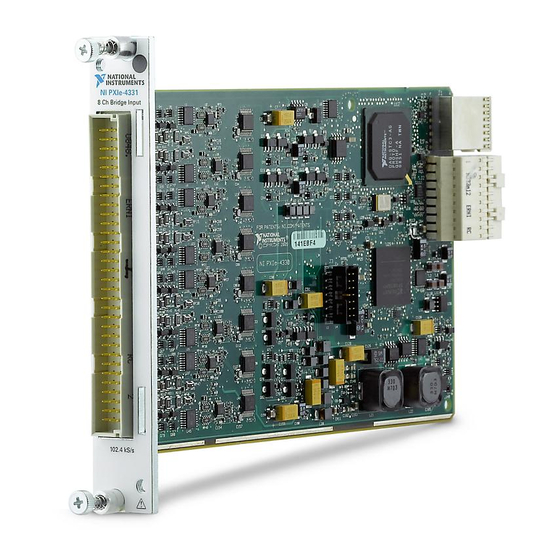
- Page 1 NI SC Express NI PXIe-4330/4331 User Manual NI PXIe-4330/4331 User Manual April 2010 373029A-01...
- Page 2 Thailand 662 278 6777, Turkey 90 212 279 3031, United Kingdom 44 (0) 1635 523545 For further support information, refer to the Technical Support and Professional Services appendix. To comment on National Instruments documentation, refer to the National Instruments Web site at and enter ni.com/info the Info Code feedback ©...
-
Page 3: Important Information
Instruments Corporation. National Instruments respects the intellectual property of others, and we ask our users to do the same. NI software is protected by copyright and other intellectual property laws. Where NI software may be used to reproduce software or other materials belonging to others, you may use NI software only to reproduce materials that you may reproduce in accordance with the terms of any applicable license or other legal restriction. -
Page 4: Table Of Contents
Signal Acquisition Considerations.................2-25 Software Scaling and Equations ............2-26 Nyquist Frequency and Nyquist Bandwidth............2-26 ADC.........................2-26 Analog Input Filters..................2-27 Anti-Alias Filters................2-27 Passband....................2-28 Stopband....................2-28 Alias-Free Bandwidth ...............2-28 Filter Group Delay ................2-28 Supported Data Rates ..................2-29 © National Instruments Corporation NI PXIe-4330/4331 User Manual... - Page 5 Contents Timing and Triggering ..................2-29 Sample Clock Timebase ..............2-29 External Clock .................. 2-29 Digital Triggering ................2-30 Analog Triggering ................2-30 Triggering and Filter Delay .............. 2-33 Synchronization ....................2-33 Reference Clock Synchronization ............ 2-33 TEDS....................... 2-35 Configuring and Using TEDS in Software........2-35 Accessory Auto-Detection ................
- Page 6 Analog Edge Triggering with Hysteresis on Falling Slope....2-32 Figure 2-23. Window Triggering ................2-32 Tables Table 2-1. Front Connector Signal Pin Assignments ..........2-22 Table 2-2. I/O Connector Signal Descriptions............2-23 Table 3-1. PXIe_DSTAR Line Descriptions ............3-2 Table 3-2. Filters.....................3-3 © National Instruments Corporation NI PXIe-4330/4331 User Manual...
-
Page 7: Getting Started
Refer to the NI PXIe-4330/4331 Specifications document for module specifications. Module Accessories and Cables Refer to the NI SC Express 4330/4331 Installation Guide and Terminal Block Specifications document for information about supported accessories and cables. © National Instruments Corporation NI PXIe-4330/4331 User Manual... -
Page 8: Using The Module
However, common strain gage configurations include one, two or four active sensing elements. Figure 2-1 shows a resistive Wheatstone bridge circuit diagram. – Figure 2-1. Basic Wheatstone Bridge Circuit Diagram © National Instruments Corporation NI PXIe-4330/4331 User Manual... -
Page 9: Connection Options To Correct For Resistance Errors
Chapter 2 Using the Module The Wheatstone bridge is the electrical equivalent of two parallel voltage divider circuits. R and R compose one voltage divider circuit, and R and R compose the second voltage divider circuit. The output of a Wheatstone bridge is measured between the middle nodes of the two voltage dividers. -
Page 10: Figure 2-2. Connecting Remote Sense Wires To The Ni Pxie-4330/4331
If you connect the remote sense signals directly to the bridge resistors, the NI PXIe-4330/4331 senses the actual bridge voltage using high-impedance RS leads and eliminates the gain errors caused by the resistance of the EX+ and EX– leads. © National Instruments Corporation NI PXIe-4330/4331 User Manual... -
Page 11: Shunt Calibration
Chapter 2 Using the Module Shunt Calibration Shunt calibration can correct for errors from the resistance of both the excitation wiring and wiring in the individual resistors of the bridge. Remote sensing corrects for resistances from the EX leads on the NI PXIe-4330/4331 to the sensor, and shunt calibration corrects for these errors and for errors caused by wire resistance within an arm of the bridge. -
Page 12: Figure 2-4. Quarter-Bridge I Circuit Diagram
—Measured voltage of the bridge. • —Excitation voltage provided by the NI PXIe-4330/4331. • —Offset compensated ratiometric bridge output defined by the following equation: strained unstrained – --------------------------------------------------------------------------------- © National Instruments Corporation NI PXIe-4330/4331 User Manual... -
Page 13: Quarter-Bridge Type Ii
Chapter 2 Using the Module The ratio of the bridge output voltage and the excitation voltage is done internally Note on the NI PXIe-4330/4331. To convert module readings to strain use the following equation: – strain ε ( ) ------------------------------- GF 1 To compensate for lead resistance errors shunt calibration should be used. -
Page 14: Figure 2-6. Quarter-Bridge Ii Circuit Diagram
—Offset compensated ratiometric bridge output defined by the following equation: strained unstrained – --------------------------------------------------------------------------------- Note The ratio of the bridge output voltage and the excitation voltage is done internally on the NI PXIe-4330/4331. © National Instruments Corporation NI PXIe-4330/4331 User Manual... -
Page 15: Half-Bridge Type I
Chapter 2 Using the Module To convert module readings to strain use the following equation: – strain ε ( ) ------------------------------- GF 1 Half-Bridge Type I This section provides information for the half-bridge strain-gage configuration type I. The half-bridge type I measures either axial or bending strain. Figure 2-7 shows how to position strain-gage resistors in an axial and bending configurations. -
Page 16: Figure 2-8. Half-Bridge Type I Circuit Diagram
—Measured voltage of the bridge. • —Excitation voltage provided by the NI PXIe-4330/4331. • —Offset compensated ratiometric bridge output defined by the following equation: (strained) V (unstrained) – --------------------------------------------------------------------------------- - © National Instruments Corporation NI PXIe-4330/4331 User Manual... -
Page 17: Half-Bridge Type Ii
Chapter 2 Using the Module The ratio of the bridge output voltage and the excitation voltage is done internally Note on the NI PXIe-4330/4331. To convert module readings to strain use the following equation: – strain ε ( ) -------------------------------------------------------------- - ν... -
Page 18: Figure 2-10. Half-Bridge Type Ii Circuit Diagram
—Offset compensated ratiometric bridge output defined by the following equation: strained unstrained – --------------------------------------------------------------------------------- The ratio of the bridge output voltage and the excitation voltage is done internally Note on the NI PXIe-4330/4331. © National Instruments Corporation 2-11 NI PXIe-4330/4331 User Manual... -
Page 19: Full-Bridge Type I
Chapter 2 Using the Module To convert module readings to strain use the following equation: – strain (ε ) ----------- - Full-Bridge Type I This section provides information for the full-bridge strain-gage configuration type I. The full-bridge type I only measures bending strain. Figure 2-11 shows how to position strain-gage resistors in a bending configuration. -
Page 20: Figure 2-12. Full-Bridge Type I Circuit Diagram
—Offset compensated ratiometric bridge output defined by the following equation: strained unstrained – --------------------------------------------------------------------------------- Note The ratio of the bridge output voltage and the excitation voltage is done internally on the NI PXIe-4330/4331. © National Instruments Corporation 2-13 NI PXIe-4330/4331 User Manual... -
Page 21: Full-Bridge Type Ii
Chapter 2 Using the Module To convert module readings to strain use the following equation: – strain (ε ) ------- - Full-Bridge Type II This section provides information for the full-bridge type II strain-gage configuration. The full-bridge type II only measures bending strain. Figure 2-13 shows how to position strain-gage resistors in a bending configuration. -
Page 22: Figure 2-14. Full-Bridge Type Ii Circuit Diagram
—Measured voltage of the bridge. • —Excitation voltage provided by the NI PXIe-4330/4331. • —Offset compensated ratiometric bridge output defined by the following equation: strained unstrained – --------------------------------------------------------------------------------- © National Instruments Corporation 2-15 NI PXIe-4330/4331 User Manual... -
Page 23: Full-Bridge Type Iii
Chapter 2 Using the Module The ratio of the bridge output voltage and the excitation voltage is done internally Note on the NI PXIe-4330/4331. To convert module readings to strain use the following equation: – strain ε ( ) ------------------------- - ν... -
Page 24: Figure 2-16. Full-Bridge Type Iii Circuit Diagram
—Measured voltage of the bridge. • —Excitation voltage provided by the NI PXIe-4330/4331. • —Offset compensated ratiometric bridge output defined by the following equation: strained unstrained – --------------------------------------------------------------------------------- © National Instruments Corporation 2-17 NI PXIe-4330/4331 User Manual... -
Page 25: Force, Pressure, And Torque Sensor Configurations
Chapter 2 Using the Module The ratio of the bridge output voltage and the excitation voltage is done internally Note on the NI PXIe-4330/4331. To convert module readings to strain use the following equation: 2 – V strain ε ( ) ---------------------------------------------------------- - GF ν... - Page 26 Some sensor calibration certificates specify the electrical output in mV or V, not mV/V or V/V. If this is the case, divide the specified electrical output by the excitation voltage at which the calibration was performed. © National Instruments Corporation 2-19 NI PXIe-4330/4331 User Manual...
-
Page 27: Common-Mode Voltage Considerations
Chapter 2 Using the Module The two-point linear conversion uses the following equations: physical physical – ------------------------------------------------------------- - electrical electrical – × physical electrical – × physical reading If offset nulling (bridge balancing) is used to compensate for offset, then the zero point of the sensor can be assumed to output exactly 0 V/V, simplifying these equations: physical --------------------------- -... -
Page 28: Shielding And Grounding Considerations
This is the pinout represented on the front connector of the NI PXIe-4330/4331. Refer to the I/O Connector Signal Description section for definitions of each signal. Refer to the terminal block installation guide for signal locations on the terminal block. © National Instruments Corporation 2-21 NI PXIe-4330/4331 User Manual... -
Page 29: Table 2-1. Front Connector Signal Pin Assignments
Chapter 2 Using the Module Table 2-1. Front Connector Signal Pin Assignments Front Connector Diagram Pin Number Column A Column B Column C Channel AIGND Column QTR/SC EX– AI– QTR/SC RS– AIGND QTR/SC EX– AI– QTR/SC RS– AIGND QTR/SC EX– AI–... -
Page 30: I/O Connector Signal Description
(RS+ and RS–) and fed back to the ADC (Analog-to-Digital Converter) reference through a programmable gain amplifier. The gain applied when sensing the excitation voltage is automatically selected based on the selected excitation voltage level. © National Instruments Corporation 2-23 NI PXIe-4330/4331 User Manual... -
Page 31: Figure 2-18. Ni Pxie-4330/4331 Signal Conditioning Block Diagram
Chapter 2 Using the Module Connector EX + Programmable Excitation – RS + Gain=1 or 0.25 RS – EX – AI + Reference Analog Anti-Alias G=10 Input AI – Filter QTR/ 120 Ω 350 Ω 1 kΩ 50 kΩ 100 kΩ EX –... -
Page 32: Signal Acquisition Considerations
Analog Trigger event from the digitized analog data of its ADCs. Signal Acquisition Considerations This section contains information about signal acquisition concepts, including software scaling and equations, Delta-Sigma converters, Nyquist frequency and bandwidth, timing, triggering, and synchronization. © National Instruments Corporation 2-25 NI PXIe-4330/4331 User Manual... -
Page 33: Software Scaling And Equations
Chapter 2 Using the Module Software Scaling and Equations After you have acquired the signal of interest, you can scale this measurement to the appropriate units in software. This is done automatically for you in NI-DAQmx using a strain task or strain channel. You also can scale the measurements manually in your application using the measurement-to-strain conversion equations provided in this document for each configuration type. -
Page 34: Analog Input Filters
While the frequency response of the digital filter directly scales with the sample rate, the analog filter –3dB point is fixed. The NI PXIe-4330/4331 automatically adjusts its oversample rate to maintain a high level of alias protection regardless of the current sampling rate. © National Instruments Corporation 2-27 NI PXIe-4330/4331 User Manual... -
Page 35: Passband
Chapter 2 Using the Module Passband The signals within the passband have frequency-dependent gain or attenuation. The small amount of variation in gain with respect to frequency is called the passband flatness. The digital filters of the NI PXIe-4330/4331 adjust the frequency range of the passband to match the sample rate. -
Page 36: Supported Data Rates
However, signal processing features in the Sound and Vibration Measurement Suite often provide an excellent alternative to external clocking in encoder and tachometer applications. Visit for more information about the Sound ni.com/soundandvibration and Vibration Measurement Suite. © National Instruments Corporation 2-29 NI PXIe-4330/4331 User Manual... -
Page 37: Digital Triggering
Chapter 2 Using the Module Digital Triggering You can configure the NI PXIe-4330/4331 modules to start an acquisition in response to a digital trigger signal from one of the PXI Express backplane trigger lines. The trigger circuit can respond either to a rising or a falling edge. In addition, the trigger circuit provides a programmable filter useful for debouncing noisy trigger signals. -
Page 38: Figure 2-20. Analog Level Trigger On Rising Slope
2.2 mV/V, as shown in Figure 2-21. 3.2 mV/V Level Hysteresis 2.2 mV/V Analog Comparison Reference Trigger Figure 2-21. Analog Edge Triggering with Hysteresis on Rising Slope © National Instruments Corporation 2-31 NI PXIe-4330/4331 User Manual... -
Page 39: Figure 2-22. Analog Edge Triggering With Hysteresis On Falling Slope
Chapter 2 Using the Module When using hysteresis with a falling slope, the trigger is armed when the signal starts above Level plus the hysteresis value and asserts when the signal crosses below Level. For example, if you add a hysteresis of 1 mV/V to a level of 3.2 mV/V, the signal must start at or rise above 4.2 mV/V to arm the trigger. -
Page 40: Triggering And Filter Delay
When you acquire data from multiple modules within the same NI-DAQmx task, NI-DAQmx will automatically handle all of the Reference Clock Synchronization details required to synchronize the modules within the task. This is known as a Multi-Device Task. © National Instruments Corporation 2-33 NI PXIe-4330/4331 User Manual... - Page 41 Chapter 2 Using the Module To perform Reference Clock Synchronization when using multiple NI-DAQmx tasks that are acquiring at the same rate, complete the following steps to synchronize the hardware. Specify PXIe_CLK100 as the reference clock source for all modules to force all the modules to lock to the reference clock on the PXIe chassis.
-
Page 42: Teds
NI-DAQmx property nodes can be used to programmatically access information about connected accessories in your application. Refer to the NI-DAQmx Help for documentation about programmatically accessing accessory status. Select Start»All Programs»National Instruments»NI-DAQ»NI-DAQmx Help. © National Instruments Corporation 2-35 NI PXIe-4330/4331 User Manual... -
Page 43: Ni Sc Express Considerations
Triggers can be used to synchronize the operation of several different PXI peripheral modules. © National Instruments Corporation NI PXIe-4330/4331 User Manual... -
Page 44: Pxie_Dstar
Chapter 3 NI SC Express Considerations On SC Express modules, the eight PXI trigger signals are synonymous with RTSI <0..7>. In a PXI chassis with more than eight slots, the PXI trigger lines may be divided into multiple independent buses. Refer to the documentation for your chassis for details. PXI_STAR Trigger In a PXI Express system, the Star Trigger bus implements a dedicated trigger line between the system timing slot and the other peripheral slots. -
Page 45: Trigger Filters
5.12 μs filter will reject any pulses shorter than 5.12 μs. The trigger filters can be used to prevent false triggers from occurring in cases where the trigger signal is noisy or glitchy. © National Instruments Corporation NI PXIe-4330/4331 User Manual... -
Page 46: Offset Nulling (Bridge Balancing)
NI PXIe-4330/4331 does not have any internal hardware nulling circuitry, however, its input range is sufficiently wide so that the inputs will not saturate even with a relatively large initial bridge offset. © National Instruments Corporation NI PXIe-4330/4331 User Manual... -
Page 47: Technical Support And Professional Services
Technical Support and Professional Services Visit the following sections of the award-winning National Instruments Web site at ni.com for technical support and professional services: • Support—Technical support at includes the following resources: ni.com/support – Self-Help Technical Resources—For answers and solutions, visit ni.com/... - Page 48 Appendix B Technical Support and Professional Services this manual. You also can visit the Worldwide Offices section of ni.com/niglobal access the branch office Web sites, which provide up-to-date contact information, support phone numbers, email addresses, and current events. NI PXIe-4330/4331 User Manual ni.com...