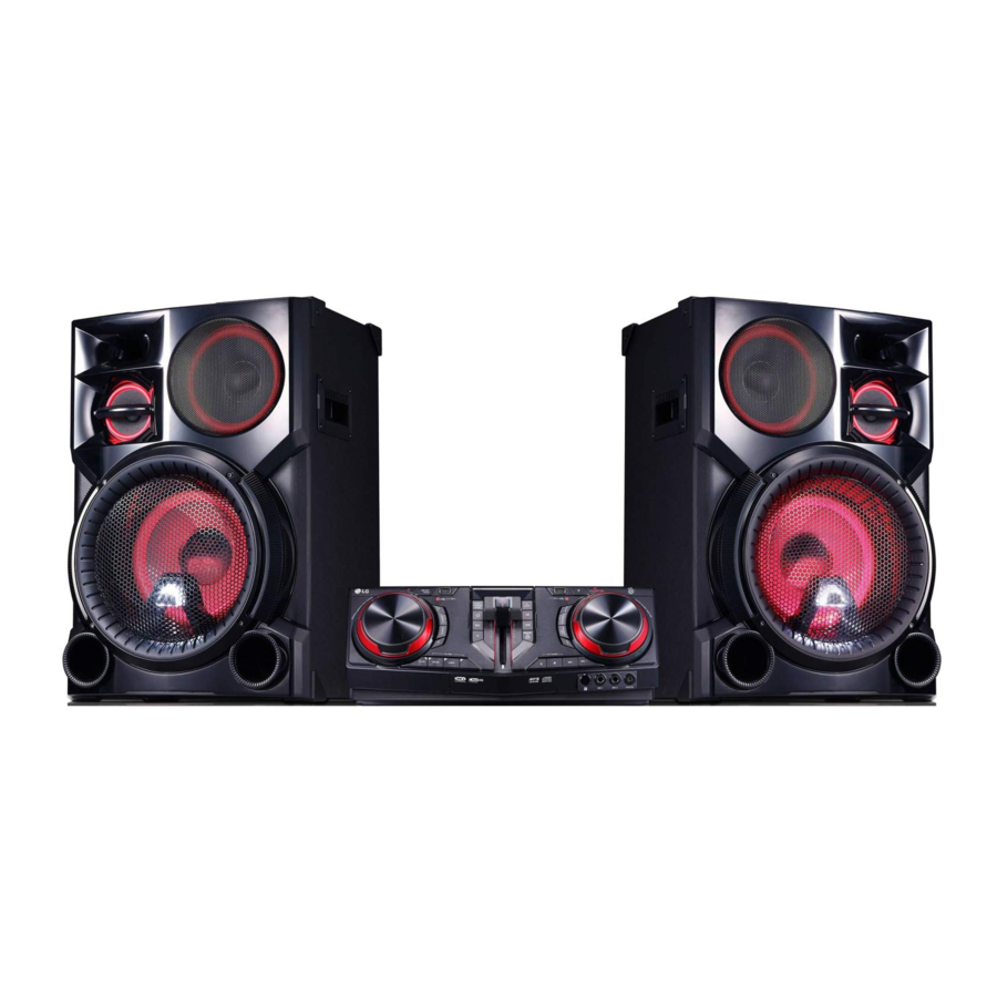
LG CJ98 Service Manual
Hide thumbs
Also See for CJ98:
- Simple manual (4 pages) ,
- Owner's manual (47 pages) ,
- Service bulletin (26 pages)

Related Manuals for LG CJ98


Summary of Contents for LG CJ98
- Page 1 Internal Use Only MINI HI-FI SYSTEM SERVICE MANUAL MODEL: CJ98 (CJ98, CJS98F) CAUTION BEFORE SERVICING THE UNIT, READ THE “SAFETY PRECAUTIONS” IN THIS MANUAL. P/NO : AFN77612177 FEBRUARY, 2017...
- Page 2 CONTENTS SECTION 1 ..GENERAL SECTION 2 ..CABINET & MAIN CHASSIS SECTION 3 ..ELECTRICAL SECTION 4 ..MECHANISM (DM14B) SECTION 5 ..REPLACEMENT PARTS LIST...
-
Page 3: Table Of Contents
SECTION 1 SUMMARY CONTENTS SERVICING PRECAUTIONS ..........................1-3 ESD PRECAUTIONS ............................1-5 HIDDEN KEY MODE ............................1-6 1. HIDDEN KEY MODE TABLE ........................1-6 2. HIDDEN KEY MODE DESCRIPTION ....................... 1-7 SERVICE INFORMATION FOR EEPROM ......................1-9 PROGRAM DOWNLOAD GUIDE ........................1-10 FOTA UPDATE STEP USING BT APP ...................... -
Page 4: Servicing Precautions
SERVICING PRECAUTIONS NOTES REGARDING HANDLING OF THE PICK-UP 1. Notes for transport and storage 1) The pick-up should always be left in its conductive bag until immediately prior to use. 2) The pick-up should never be subjected to external pressure or impact. Storage in conductive bag Drop impact 2. - Page 5 NOTES REGARDING COMPACT DISC PLAYER REPAIRS 1. Preparations 1) Compact disc players incorporate a great many ICs as well as the pick-up (laser diode). These components are sensitive to, and easily affected by, static electricity. If such static electricity is high voltage, components can be damaged, and for that reason components should be handled with care.
-
Page 6: Esd Precautions
ESD PRECAUTIONS Electrostatically Sensitive Devices (ESD) Some semiconductor (solid state) devices can be damaged easily by static electricity. Such components commonly are called Electrostatically Sensitive Devices (ESD). Examples of typical ESD devices are integrated circuits and some field-effect transistors and semiconductor chip components. The following techniques should be used to help reduce the incidence of component damage caused by static electricity. -
Page 7: Hidden Key Mode
HIDDEN KEY MODE 1. HIDDEN KEY MODE TABLE HIDDEN MODE ENTRANCE KEY(Audio) EXIT KEY Front ‘Stop’ Version Check Remote Control Key ‘Play’ for 1.5s + Remote Control Key ‘Play’ for 5s Front ‘Stop’ EEPROM INITIAL Auto exit + Remote Control Key ‘ ‘... -
Page 8: Hidden Key Mode Description
2. HIDDEN KEY MODE DESCRIPTION 2-1. Version Check - Function : Version Check. - Entrance Key : Front ‘Stop’ + Remote Control Key ‘Play’ for 5s. - Exit Key : Remote Control Key ‘Play’ for 1.5s. - Operation explanation : Remote Control Key VFD Display (Example) Result MCS Version... - Page 9 2-5. Disc Lock On/Off - Function : Lock Open Key. - Entrance Key : Front ‘Stop’ + Remote Control Key ‘Stop’ for 5s. - Exit Key : Front ‘Stop’ + Remote Control Key ‘Stop’ for 5s. - Operation Explain : Open Key Block ‘LOCKED’. 2-6.
-
Page 10: Service Information For Eeprom
SERVICE INFORMATION FOR EEPROM POWER ON It is possible at any function. (ex. It is possible at VFD “NO USB” status, too.) VFD “NO DISC” status This is an example. Front ‘Stop’ + Remote control ‘ ’ DETECT NEW EEPROM push same timing during 5 s (OPTION EDIT SCREEN) NAME... -
Page 11: Program Download Guide
PROGRAM DOWNLOAD GUIDE 1. AUDIO PROGRAM Download program file name must be MICOM_CJ98_YYMMDDX.HEX If security program(Water Wall) is activated on PC, you must save the file to the USB storage device and disable the security software, then download the file to your set. Downloading file proceeds in the same way at USB1 function and USB2 function. - Page 12 2. CD PROGRAM Download program file name must be HG790_CJ98_YYMMDDX.bin If security program(Water Wall) is activated on PC, you must save the file to the USB storage device and disable the security software, then download the file to your set. Downloading file proceeds in the same way at USB1 function and USB2 function.
- Page 13 3. EQ & DEMO PROGRAM Download program file name must be EQ_DEMO_PRG_CJ98_XXXX.BIN If security program(Water Wall) is activated on PC, you must save the file to the USB storage device and disable the security software, then download the file to your set. Downloading file proceeds in the same way at USB1 function and USB2 function.
-
Page 14: Fota Update Step Using Bt App
FOTA UPDATE STEP USING BT APP Step1 : App connecting Step2 : Device version info (Check FW version) After connecting the BT App with SET, When touch the “Device Version info” button, the user could fi nd the “Device Version info” on user could fi... - Page 15 Step5 : Download from CDN server Step6 : Transfer FW 1st step is download from CDN server to After completed the download from server, smart phone. The progress bar is displayed smart phone start to transfer the fi rmware to the on BT App.
-
Page 16: Specifications
SPECIFICATIONS GENERAL Power requirements Refer to the main label on the unit. Power consumption Refer to the main label on the unit. Networked standby : 0.5 W (If all network ports are activated.) Dimensions (W x H x D) Approx. - Page 17 1-16...
- Page 18 SECTION 2 CABINET & MAIN CHASSIS CONTENTS EXPLODED VIEWS ............................2-3 1. CABINET AND MAIN FRAME SECTION ....................2-3 2. PACKING ACCESSORY SECTION ......................2-7 3. SPEAKER SECTION ..........................2-8 DISASSEMBLY INSTRUCTIONS ........................2-9 1. Case Top ..............................2-9 2. Panel Front Assembly ..........................2-9 3.
-
Page 20: Exploded Views
EXPLODED VIEWS 1. CABINET AND MAIN FRAME SECTION NOTES) THE EXCLAMATION POINT WITHIN AN EQUILATERAL TRIANGLE IS INTENDED TO ALERT THE SERVICE PERSONNEL TO THE PRESENCE OF IMPORTANT SAFETY INFORMATION IN SERVICE LITERATURE. SMPS MAIN FRONT CABLE2 CABLE1 CABLE3... -
Page 22: Packing Accessory Section
2. PACKING ACCESSORY SECTION 801 Owner’s manual Battries 826 Filter, Ferrite Core 900 Remote control FM antenna Packing 804 Bag 802 Box... -
Page 23: Speaker Section
3. SPEAKER SECTION • FRONT SPEAKER A60L A60R... -
Page 24: Disassembly Instructions
DISASSEMBLY INSTRUCTIONS 1. Case Top 1-1) Remove the 7 Screws. 1-2) Remove the Case Top. Figure 1 2. Panel Front Assembly 2-1) Disconnect the 4 FFC Cables from the Main Board. 2-2) Unhook the 10 Locking Tabs by using Flat-head screwdriver. 2-3) Remove the Panel Front Assembly. -
Page 25: Panel Pcb & Multi Knob
3. Panel PCB & Multi Knob 3-1) Multi Knob 3-1-1) Insert a Flat-head screwdriver in the hole (H1). 3-1-2) Remove the Multi Knob. 3-2) Jack PCB 3-2-1) Remove the 2 Screws. 3-2-2) Remove the Jack PCB. 3-3) BT Module 3-3-1) Unhook the Locking tab (L1). 3-3-2) Remove the BT Module. -
Page 26: Bracket Hook
4. Bracket Hook 4-1) Remove the 2 Screws. 4-2) Rotate 90 degrees to the front. 4-3) Remove the Bracket Hook. Figure 4 2-11... -
Page 27: Main Pcb & Smps Pcb
5. Main PCB & SMPS PCB 5-1) Remove the 2 Screws from the Panel Rear. 5-2) Disconnect the 4 FFC Cables from the Main Board. 5-3) Remove the 10 Screws from the Main Board & SMPS Board. 5-4) Remove the Main Board & SMPS Board. Figure 5 2-12... -
Page 28: Bracket Inner
6. Bracket Inner 6-1) Remove the 2 Screws from the Panel Rear. 6-2) Remove the 2 Screws from the Bracket Inner. 6-3) Remove the Bracket Inner. Figure 6 2-13... -
Page 29: Md & Lighting Pcb
7. MD & Lighting PCB 7-1) Remove the 2 Screws from the MD. 7-2) Remove the 2 Screws from the Lighting PCB. 7-3) Remove the MD & Lighting PCB. Figure 7 8. Panel Rear 8-1) Remove the 1 Screw from the Panel Rear. 8-2) Remove the Panel Rear. - Page 30 SECTION 3 ELECTRICAL CONTENTS ONE POINT REPAIR GUIDE ..........................3-2 1. NO POWER ............................3-2 2. NO BOOTING WHEN POWER ON THE SET..................3-4 3. NO BOOTING IN CD/USB FUNCTION ....................3-5 4. NO OPERATION OF MD ........................3-10 5. NO SOUND IN THE USB FUNCTION ....................3-15 6.
-
Page 31: One Point Repair Guide
ONE POINT REPAIR GUIDE 1. NO POWER If the unit doesn’t work by no power problem, repair the set according to the following guide. 1-1. POWER 1-1-1. Solution Please check and replace F901, BD901 and TH900 ~ TH903 on SMPS board. 1-1-2. - Page 32 ONE POINT REPAIR GUIDE NO POWER If the unit doesn’t work by no ±PVDD problem, repair the set according to the following guide. 1-2. AMP POWER 1-2-1. Solution Please check and replace F911, Q905, Q906 on SMPS board. 1-2-2. How to troubleshoot (Countermeasure) 1) Check if the fuse F911 is open or short-circuit.
-
Page 33: No Booting When Power On The Set
ONE POINT REPAIR GUIDE 2. NO BOOTING WHEN POWER ON THE SET The set doesn’t work when press the power button on the FRONT board or the remote control. 2-1. IC501 2-1-1. Solution Replace IC501 on MAIN board. 2-1-2. How to troubleshoot (Countermeasure) 1) Check the 5.6 VA(CN300) and DVCC 3.3 V(IC306) in standby mode. - Page 34 ONE POINT REPAIR GUIDE 3. NO BOOTING IN CD/USB FUNCTION After you turn on power key and displayed message in the following order (HELLO VOL XX CD or USB) on VFD, it will not display other message on VFD, and it will not boot-up normally. 3-1.
-
Page 35: No Booting In Cd/Usb Function
ONE POINT REPAIR GUIDE NO BOOTING IN CD/USB FUNCTION After you turn on power key and displayed message in the following order (HELLO VOL XX CD or USB) on VFD, it will not display other message on VFD, and it will not boot-up normally. 3-2. - Page 36 ONE POINT REPAIR GUIDE NO BOOTING IN CD/USB FUNCTION After you turn on power key and displayed message in the following order (HELLO VOL XX CD or USB) on VFD, it will not display other message on VFD, and it will not boot-up normally. 3-3.
- Page 37 ONE POINT REPAIR GUIDE NO BOOTING IN CD/USB FUNCTION After you turn on power key and displayed message in the following order (HELLO VOL XX CD or USB) on VFD, it will not display other message on VFD, and it will not boot-up normally. 3-4.
- Page 38 ONE POINT REPAIR GUIDE NO BOOTING IN CD/USB FUNCTION After you turn on power key and displayed message in the following order (HELLO VOL XX CD or USB) on VFD, it will not display other message on VFD, and it will not boot-up normally. 3-5.
- Page 39 ONE POINT REPAIR GUIDE 4. NO OPERATION OF MD When no sound output in the CD function, you can not listen to music reading data from a CD disc if the servo motors in MD don’t work. This step is for checking the spindle motor among them. 4-1.
-
Page 40: No Operation Of Md
ONE POINT REPAIR GUIDE NO OPERATION OF MD When no sound output in the CD function, you can not listen to music reading data from a CD disc if the servo motors in MD don’t work. This step is for checking the sled motor among them. 4-2. - Page 41 ONE POINT REPAIR GUIDE NO OPERATION OF MD When no sound output in the CD function, you can not listen to music reading data from a CD disc if the servo motors in MD don’t work. This step is for checking the tray open/close motor among them. 4-3.
- Page 42 ONE POINT REPAIR GUIDE NO OPERATION OF MD When no sound output in the CD function, you can not listen to music reading data from a CD disc if the pickup module in MD doesn’t work. This step is for checking the laser tracking actuator. 4-4.
- Page 43 ONE POINT REPAIR GUIDE NO OPERATION OF MD When no sound output in the CD function, you can not listen to music reading data from a CD disc if the pickup module in MD doesn’t work. This step is for checking the laser focusing actuator. 4-5.
-
Page 44: No Sound In The Usb Function
ONE POINT REPAIR GUIDE 5. NO SOUND IN THE USB FUNCTION There is no sound output in the USB function, repair the set according to the following guide. 5-1. USB FUNCTION 5-1-1. Solution Replace IC501 or IC303 on MAIN board. 5-1-2. -
Page 45: Audio Output Is Small Or No Audio Output
ONE POINT REPAIR GUIDE 6. AUDIO OUTPUT IS SMALL OR NO AUDIO OUTPUT Audio signal output is small or not. when you power on the middle power mini system. 6-1. AMP IC (IC700 ~ IC702, IC800 ~ IC802) 6-1-1. Solution Replace IC700 ~ IC702, IC800 ~ IC802 on MAIN board. -
Page 46: No Power On (Standby Led Is Blinking)
ONE POINT REPAIR GUIDE 7. NO POWER ON (STANDBY LED IS BLINKING) It doesn’t turn on, and blinks standby LED (RED). 7-1. AMP FETs 7-1-1. Solution Replace AMP FET on MAIN board. 7-1-2. How to troubleshoot (Countermeasure) 1) This symptom occurs, when DC protection is detected. MAIN reasons are like below. - When some of AMP FETs dead. -
Page 47: Speaker No Audio
ONE POINT REPAIR GUIDE 8. SPEAKER NO AUDIO Speaker no audio. 8-1. AMP IC (IC700 ~ IC702, IC800 ~ IC802) 8-1-1. Solution Replace IC700 ~ IC702, IC800 ~ IC802 on MAIN board. 8-1-2. How to troubleshoot (Countermeasure) 1) Check supply voltage of AMP(CN800) & PWM signal Normal supply voltage and signal ... - Page 48 ONE POINT REPAIR GUIDE 9. NO SOUND There is no sound output in the AUX function, repair the set according to the following guide. 9-1. AUX FUNCTION 9-1-1. Solution Replace IC200 on MAIN board. 9-1-2. How to troubleshoot (Countermeasure) 1) Check AUX_L/R signals to IC200(pin3, pin4). 2) Check if MCS_BCK, MCS_LRCK, &...
-
Page 49: No Sound
ONE POINT REPAIR GUIDE NO SOUND There is no sound output in the PORT. IN function, repair the set according to the following guide. 9-2. PORT. IN FUNCTION 9-2-1. Solution Replace IC200 on MAIN board. 9-2-2. How to troubleshoot (Countermeasure) 1) Check PT_L/ R signal from FRONT board to MAIN board. - Page 50 ONE POINT REPAIR GUIDE NO SOUND There is no sound output in the TUNER function, repair the set according to the following guide. 9-3. TUNER FUNCTION 9-3-1. Solution Replace IC200, TU500 on MAIN board. 9-3-2. How to troubleshoot (Countermeasure) 1) Check if TUNER_LR is entered from pin1 & pin3 of TU200 to IC200(pin1, pin2). ...
- Page 51 ONE POINT REPAIR GUIDE NO SOUND There is no sound output in the MIC IN function, repair the set according to the following guide. 9-4. MIC IN FUNCTION 9-4-1. Solution Replace IC200, IC201 on MAIN board. 9-4-2. How to troubleshoot (Countermeasure) 1) Check MIC_SIG signal to pin6 of CN200.
- Page 52 ONE POINT REPAIR GUIDE NO SOUND There is no sound output in the Bluetooth function, repair the set according to the following guide. 9-5. BLUETOOTH FUNCTION 9-5-1. Solution Replace IC501 on the MAIN board or bluetooth module on the FRONT Panel. 9-5-2.
-
Page 53: Vfd Is Not Displayed When Power On The Set
ONE POINT REPAIR GUIDE 10. VFD IS NOT DISPLAYED WHEN POWER ON THE SET When power on the set, any icons or characters on VFD are not displayed. 10-1. VFD (VFD301) 10-1-1. Solution Please check and replace VFD301 on FRONT board. 10-1-2. -
Page 54: Electrical Troubleshooting Guide
ELECTRICAL TROUBLESHOOTING GUIDE 1. POWER SUPPLY ON SMPS BOARD No output 5.1 VA Replace F901 (same fuse). Is the F901 normal? Replace BD901. Is BD901 normal? Is the VCC Is D960, D961 normal? (11 V ~ 25 V) supplied to IC901 pin4? Power line of MAIN PCB is short. -
Page 55: Power Supply On Smps Board
ELECTRICAL TROUBLESHOOTING GUIDE POWER SUPPLY ON SMPS BOARD No -5 V Is the Is the D959 normal? Check or replace D959. VCC -7 VA supplied to IC953 pin2? Check or replace Q951. Is there Check P_CTL ‘H’ signal at Q953 from μ-com. - Page 56 ELECTRICAL TROUBLESHOOTING GUIDE POWER SUPPLY ON SMPS BOARD No AMP output Is the Check PFC P.CTL Is the C904 voltage PFC P.CTL OK? from μ-com. about 390 V? Is the VCC 12 V supplied to Replace D908, Q955, PC903. IC904 pin16? Check or replace IC904, Q907 ~ Q910.
-
Page 57: System Part
ELECTRICAL TROUBLESHOOTING GUIDE 2. SYSTEM PART Power on. CN101 “HELLO” cable connection Display on FLD Check FFC cable. CN101 pin11, 22, 25,power Check SMPS board. CN101 pin5, 6, 7 data signal Check MAIN board. F+/- & VH voltage OK? Replace VFD301. Check When turn CN101 pin3, 4 I2C data... - Page 58 ELECTRICAL TROUBLESHOOTING GUIDE 3. NO AUDIO CHECK CD FUNCTION Is Motor_open/ close OK? LOAD +, - OK? disc insert? (IC400 pin6, 7) Check IC501. Is motor impedance Check loading motor. about 12 Ω? Check IC400. Focusing/ OPU driving Tracking/ Sled signal Disc reading OK? (Focusing &...
-
Page 59: No Audio Check
ELECTRICAL TROUBLESHOOTING GUIDE NO AUDIO CHECK USB play IC303 When insert USB, USB power USB_5 V Replace IC303. IC501 pin U7, U8, A7, A8 USB_D signal OK? IC200 Check audio cable. pin 3, 4 AUX input signal IC200 Check IC501. pin15, 16, 17 I2S input signal IC200 Replace IC200. - Page 60 ELECTRICAL TROUBLESHOOTING GUIDE NO AUDIO CHECK POT. IN IC200 Check FRONT board. pin29, 30 POT. IN input signal IC200 Check IC501. pin15, 16, 17 I2S input signal IC200 pin18 Replace IC200. ADC_data output signal TUNER TUN200 IC200 pin1, 2 TUNER_L/R output TUNER_L/R input signal Check +3.3 V of TUN200.
- Page 61 ELECTRICAL TROUBLESHOOTING GUIDE NO AUDIO CHECK IC501 Check IC501. pin D1,D2,E1 I2S Clock signal IC501 Check IC501. pin E2 I2S data signal IC600 Replace IC600. PWM data output signal 3-32...
- Page 62 ELECTRICAL TROUBLESHOOTING GUIDE NO AUDIO CHECK Pin45, 46 of IC600 Pin39 ~ 50 of IC600 FL/FR± signal OK? SW1± signal OK? Check IC600. Check IC600. IC601,IC603 IC602 FL/FR audio signal OK? SW1 audio signal OK? Check IC601,IC603 Check IC602 Pin13 Pin13 of IC702 of IC700, IC801 FL/FR SW1 audio signal OK?
-
Page 63: No Lighting (Speaker Led)
4. NO LIGHTING (SPEAKER LED) Power On Push the “LIGHTING” button. Trun on the LED? Check Q3L01 ~ Q3L14 Check Q3L01 ~ Q3L14. LED_5 V. IC305 Check IC305. LED_5 V OK? Check speakers. 3-34... -
Page 64: Waveforms Of Major Check Point
WAVEFORMS OF MAJOR CHECK POINT 1. DSP (IC501) X X I X X I Fig 1-1. Crystal of RTC 32.768 MHz Fig 1-2. Crystal of system 24 MHz (Both ends of R561) X501 ( MAIN DSP : R551, C53B) X500 This model is not used. -
Page 65: Pwm (Ic600)
2. PWM (IC600) X X I Fig 2-1. Crystal 24.576 MHz Fig 2-2. DSP to PWM I2S (IC600 pin4, pin5) X600 (IC600 pin26 ~ pin30) 3-36... -
Page 66: Servo (Ic401)
3. SERVO (IC401) X X I Fig 3-1. Crystal 16.9344 MHz Fig 3-2. CD-16M (X400) (IC401 pin31) 3-37... -
Page 67: Motor Driver (Ic400)
4. MOTOR DRIVER (IC400) Fig 4-2. SL- & SL+ for Driving SPINDLE Motor Fig 4-1. LO- & LO+/ MOT_OPEN & (IC400 pin11, pin12) MOT_CLOSE for Driving TRAY Motor (IC400 pin6, pin7, pin9, pin10) Fig 4-3. SP- & SP+ for Driving SPINDLE Motor (IC400 pin17, pin18) 3-38... - Page 68 5. ADC 6. USB Fig 5. ADC I2S Fig 6. USB D+/ D- (IC200 pin16, pin17, pin18) (CN503 pin4, pin5, pin7, pin8) 3-39...
- Page 69 7. BLUETOOTH B B T_TX BT_TX BT_TX BT_RX BT_RX BT_RX BT_RST BT_RST BT_RST Fig 7. BT_TX/ BT_RX/ BT_RST 28 27 26 3-40...
-
Page 70: Adc
WIRING DIAGRAM AUX In Tuner SPK_L SPK_W SPK_R IC200 IC3L01 SPK LED EXPENDER MAIN IC400 SMPS Motor DR IC600 IC401 RF IC IC100 IC503 IC501 IC504 SDRAM MICOM F/S 16M module Harness FRONT Party Thruster JACK USB2 USB1 3-41 3-42... -
Page 71: Block Diagram
BLOCK DIAGRAM USB1 USB2 SCRATCH A/B, CD_RST TOP_LED, FRONT_AGL, A,B,C,D,E,F,PD (VCC50) SERVO MID_AGL, WOOFER_AGL MIC_DET, PTB_DET, P/UP SEARCH A/B CD_RW/MCLK/LRCK/BCK, SPDO/SLDO CD_DAT /FOD/TRD D2S+/ - MOT_MUTE,CLOSE,OPEN FM/AM Motor Drive LOAD± ,SLED ± , SPIN± ,TR± ,F± IC101 SPK_EXP MICOM DECK IC603 CLK/DAT/LAT OP_SW,CL_SW,UP_SW,DN_SW,D_SENSE... -
Page 72: Circuit Voltage Chart
CIRCUIT VOLTAGE CHART 1. CAPACITOR VOLTAGE 100 V - 10 % 240 V/ 50 Hz + 10 % Value Capacitor Voltage_Spec Location Measured voltage Measured voltage (uF) SMPS Board C904 270 uF 450 V C926 47 uF 50 V 7.15 C927 47 uF 50 V... -
Page 73: Printed Circuit Board Diagrams
PRINTED CIRCUIT BOARD DIAGRAMS 1. SMPS P.C.BOARD DIAGRAM (TOP VIEW) 3-47 3-48... - Page 74 SMPS P.C.BOARD DIAGRAM (BOTTOM VIEW) NOTE) Warning Parts that are critical with respect to risk of fire or electrical shock. 3-49 3-50...
-
Page 75: Main P.c.board Diagram
2. MAIN P.C.BOARD DIAGRAM (TOP VIEW) 3-51 3-52... - Page 76 MAIN P.C.BOARD DIAGRAM (BOTTOM VIEW) 3-53 3-54...
-
Page 77: Front P.c.board Diagram
3. FRONT P.C.BOARD DIAGRAM (TOP VIEW) 3-55 3-56... - Page 78 FRONT P.C.BOARD DIAGRAM (BOTTOM VIEW) 3-57 3-58...
-
Page 79: Jack P.c.board Diagram
4. JACK P.C.BOARD DIAGRAM (TOP VIEW) (BOTTOM VIEW) 5. LED CONNECTOR P.C.BOARD DIAGRAM (TOP VIEW) (BOTTOM VIEW) 3-59 3-60... - Page 80 SECTION 4 MECHANISM (DM14B) CONTENTS DECK MECHANISM DISASSEMBLY 1. Cover Top ............................... 4-2 2. Clamp Assembly ............................. 4-2 2-1. Plate ..............................4-2 2-2. Magnet ............................. 4-2 2-3. Clamp ............................... 4-2 3. Tray Disc ..............................4-3 4. Pick Up Assembly ........................... 4-4 5.
-
Page 81: Deck Mechanism Disassembly
DECK MECHANISM DISASSEMBLY (S1) Cover Top Clamp Assembly Clamp Assembly Plate Magnet Clamp (L1) < Figure A > < Figure B > 1. Cover Top 2. Clamp Assembly 1) Remove the 2 screws (S1). 1) Place the Clamp Assembly as Figure B. 2) Unhook the 4 Locking Tabs (L1) by using a 2) Bending the Cover Top in direction of flat-head screwdriver. -
Page 82: Tray Disc
DECK MECHANISM DISASSEMBLY Emergency eject hole MD Sub (H1) Assembly Tray Disc < Bottom side view > Tray Disc < Figure D > Tray Disc 3) Grasp the both sides of the Tray Disc and lift it up as Figure D, and then pull the Tray Disc <... -
Page 83: Pick Up Assembly
DECK MECHANISM DISASSEMBLY Gasket Tape Base Up/Down Deck PCB Assembly (L2) (H2) < Bottom side view > (S2) Base Main Figure G-3 Guide Rubber FFC Cable Damper Pick Up Assembly Base Up/Down Figure G-1 Figure G-2 < Figure G > 5. -
Page 84: Belt Loading
DECK MECHANISM DISASSEMBLY Base Main Figure H-1 Guide Gear Loading Gear Pulley (L3) Base Main < Bottom side view > Belt Loading (L4) Deck PCB Motor < Bottom side view > Assembly < Bottom side view > Assembly Deck PCB (S3) Assembly <... -
Page 85: Deck Mechanism Exploded View (Dm14B)
DECK MECHANISM EXPLODED VIEW (DM14B) 1439 1002 A001 1005 1001 1026 1003 1004 1030 1024 1437 1437 1024 1024 1012 1049 1437 1013 1016 1015 1024 1020 1011 A006 A005 1019 1043 1018 1045 1439...