Table of Contents
Advertisement
Quick Links
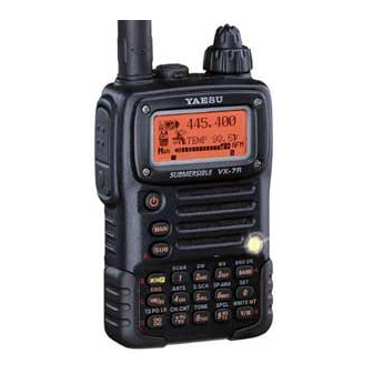
50/144/430 MHz Triple-Band
Heavy Duty Submersible Transceiver
VX-7R
Technical Supplement
©
2010 VERTEX STANDARD CO., LTD.
Specification ............................................................................................................................................ 2
Exploded View & Miscellaneous Parts ............................................................................................. 4
Block Diagram ........................................................................................................................................ 5
Interconnection Diagram ...................................................................................................................... 6
Circuit Description................................................................................................................................ 7
Alignment .............................................................................................................................................. 11
Board Unit (Schematics, Layouts & Parts)
RF Unit ............................................................................................................................................................................. 19
AF Unit ............................................................................................................................................................................ 39
CNTL Unit ....................................................................................................................................................................... 53
VCO Unit ......................................................................................................................................................................... 69
EH009M90E
the VX-7R 50/144/430 MHzTriple-Band Heavy Duty Submersible Trans-
ceiver.
chip components. Attempts by non-qualified persons to service this
equipment may result in permanent damage not covered by the war-
ranty, and may be illegal in some countries.
this transceiver. Each side of the board is referred to by the type of the
majority of components installed on that side ("Side A" or "Side B"). In
most cases one side has only chip components, and the other has either
a mixture of both chip and leaded components (trimmers, coils, electro-
DW
lytic capacitors, ICs, etc.), or leaded components only.
TEX STANDARD assumes no liability for damage that may occur as a
result of typographical or other errors that may be present. Your coop-
eration in pointing out any inconsistencies in the technical information
would be appreciated.
Contents
VERTEX STANDARD CO., LTD.
4-8-8 Nakameguro, Meguro-Ku, Tokyo 153-8644, Japan
VERTEX STANDARD
US Headquarters
10900 Walker Street, Cypress, CA 90630, U.S.A.
YAESU UK LTD.
Unit 12, Sun Valley Business Park, Winnall Close
Winchester, Hampshire, SO23 0LB, U.K.
VERTEX STANDARD HK LTD.
Unit 5, 20/F., Seaview Centre, 139-141 Hoi Bun Road,
Kwun Tong, Kowloon, Hong Kong
VERTEX STANDARD AUSTRALIA PTY., LTD.
Normanby Business Park, Unit 14/45 Normanby Road
Notting Hill 3168, Victoria, Australia
This manual provides the technical information necessary for servicing
Servicing this equipment requires expertise in handing surface-mount
Two PCB layout diagrams provided for each double-sided board in
While we believe the information in this manual to be correct, VER-
1
Advertisement
Table of Contents

Related Manuals for Vertex VX-7R


Summary of Contents for Vertex VX-7R
-
Page 1: Table Of Contents
EH009M90E Notting Hill 3168, Victoria, Australia This manual provides the technical information necessary for servicing the VX-7R 50/144/430 MHzTriple-Band Heavy Duty Submersible Trans- ceiver. Servicing this equipment requires expertise in handing surface-mount chip components. Attempts by non-qualified persons to service this equipment may result in permanent damage not covered by the war- ranty, and may be illegal in some countries. -
Page 2: Specification
Specifications General Frequency Ranges: Rx (MAIN): 0.5 - 1.8 MHz (BC Band) 1.8 - 30 MHz (SW Band) 30-59 MHz (50 MHz HAM: USA version) 30-76 MHz (50 MHz HAM: EXP version) 59-108 MHz (FM: USA version) 76-108 MHz (FM: EXP version) 108-137 MHz (Air Band) 137-174 MHz (144 MHz HAM) 174-222 MHz (VHF-TV) - Page 3 Specifications Transmitter RF Power Output: 5/2.5/1.0/0.5 W (50/144/430 MHz, FM) 0.3 W (220 MHz, FM) 1.0 W (50 MHz, FM) Modulation Type: FM: Variable Reactance AM: Early Stage (Low Level) Maximum Deviation: ±5/±2.5 kHz Spurious Emission: At least 60 dB below (@ Tx 1W) Microphone Impedance: 2 k-ohm Receiver...
-
Page 4: Exploded View & Miscellaneous Parts
Exploded View & Miscellaneous Parts Œ U9900137 BINDING HEAD SCREW M2X21.7 (W/ O RING) Ž Ž U9900138 BINDING HEAD SCREW M2X5 (W/ O RING) Ž RA0417100 Ž Ž U07225120 PAN HEAD SCREW M2X2.5SUS#1 PANEL FRAME U9900136 SPECIAL SCREW M2X2.35 ... -
Page 5: Block Diagram
Block Diagram... -
Page 6: Interconnection Diagram
Interconnection Diagram... -
Page 7: Circuit Description
Circuit Description The VX-7R consists of a RF-UNIT, a CNTL-UNIT and (3) 435-MHz Band and 222-540MHz Reception an AF-UNIT. The RF-UNIT contains the receiver front end, Received signals between 222 and 540 MHz pass PLL IC, power and switching circuits, and the VCO-UNIT through the Triplexer circuit, low-pass filter/high-pass for transmit and receive local signal oscillation. - Page 8 Circuit Description passed through a band-pass filter to first mixer Q1013 This second IF is filtered by ceramic filter CF2002 (2SC4915-0). Meanwhile, HF output from the VCO-UNIT (ALFYM450F=k) and amplified by the limiting amplifier is amplified by Q1018 and applied through diode T/R within the Narrow IF IC before quadrature detection by switch D1046 to mixer Q1013 as the first local signal.
- Page 9 Circuit Description (2) Modulation (4) 435-MHz-Band Transmission Voice signal input from either built-in microphone Modulating audio from the CNTL-UNIT passes through MC3001 (EM-140) on the CNTL-UNIT or external jack deviation setting D/A converter Q3012 to the UHF mod- J2002 on the AF-UNIT is pre-emphasized by C3012 and ulator portion of the VCO-UNIT mounted on the RF- R3031, and processed by microphone amplifier Q3018 UNIT.
- Page 10 Circuit Description phase difference between them. This pulse is fed to the PLL Frequency Synthesizer charge pump, and the output from the charge pump pass- PLL IC Q1019 on the RF-UNIT consists of a data shift es through a loop filter composed of L1044, R1089, C1175, register, reference frequency divider, phase comparator, and either R1090, C1192, R1103 and C1195 for VHF, or charge pump, "intermittent operation"...
-
Page 11: Alignment
Alignment Introduction and Precautions Required Test Equipment The VX-7R has been carefully aligned at the factory for RF Signal Generator with calibrated output level at 500 MHz the specified performance across the specified amateur Deviation Meter (linear detector) bands. Realignment should therefore not be necessary In-line Wattmeter with 5% accuracy at 500 MHz except in the event of a component failure. - Page 12 Alignment Test Setup Squelch Preset Threshold (THLD SQL) [86] Set up the test equipment as shown below for transceiv- Inject a –15.0 dBμ RF signal (1 kHz tone @ ±3.5 kHz er alignment, and apply 8.7 V DC power to the transceiver. deviation), then press the V/M button, then press the Refer to the drawings for Alignment Points.
- Page 13 Alignment L1 Tx Power Adjustment (L1 POWER) High TX Power Adjustment (L2 POWER) Transmit, and adjust the output power level for 50 mW Transmit, and adjust the output power level for 1.0 W (+50/-30 mW) by rotating the DIAL, then press the V/M (±0.1 W) by rotating the DIAL, then press the V/M but- button.
- Page 14 Alignment Squelch Preset Threshold (THLD SQL) L1 Tx Power Adjustment (L1 POWER) Inject a –15.0 dBμ RF signal (1 kHz tone @ ±3.5 kHz Transmit, and adjust the output power level for 50 mW deviation), then press the V/M button, then press the (+50/-30 mW) by rotating the DIAL, then press the V/M MON/F button twice.
- Page 15 Alignment High TX Power Adjustment (L3 POWER) Press the BAND button to activate the 145 MHz band Transmit, and adjust the output power level for 2.5 W internal alignment routine. (±0.2 W) by rotating the DIAL, then press the V/M but- The alignment frequency will automatically be set to ton.
- Page 16 Alignment High TX Power Adjustment (HI POWER) Press the MON/F to activate the TX Power and Devia- Transmit, and adjust the output power level for 5.0 W tion alignment routine. (±0.3 W) by rotating the DIAL, then press the V/M but- The alignment frequency will automatically be set to ton.
- Page 17 Alignment DCS Tx Deviation Adjustment (DCS DEV) DCS Tx Deviation Adjustment (DCS DEV) Press the V/M button, then transmit and adjust the de- Press the V/M button, then transmit and adjust the de- viation for 0.6 kHz (±0.1 kHz) by rotating the DIAL, then viation for 0.9 kHz (±0.1 kHz) by rotating DIAL, then press the V/M button.
- Page 18 Alignment Squelch Preset Tight (TIGH SQL) Press the SUB button to activate the SUB band internal alignment routine. Adjust the generator level to –4.0 dBμ, then press the V/ The alignment frequency will automatically be set to M button, then press the MON/F button twice. Press the 435.100 MHz (USA Version: 440.100 MHz) on the SUB V/M button, then rotate the DIAL to select the next set- band.
-
Page 19: Rf Unit
RF Unit (Lot. 1 ~ 2) Circuit Diagram MAIN NFM RX:+14.7dBµ (50M TX:1.84V) 435.000MHz, @12dB SINAD (144M TX:1.85V) 1000pF Coupling Capacitor. 800M RX:1.87V (430M TX:2.85V) 800M RX:0.8V 800M RX:0.73V 145M TX:+5.1dBm 800M RX:1.61V 13.5V 430M TX:+6.9dBm (13.3V) (1.86V) 1000pF Coupling Capacitor. (1.98V) (3.97V) MAIN NFM RX:+7.3dBµ... - Page 20 RF Unit (Lot. 1 ~ 2) Parts Layout Side A Side B NJM12902V MB15A01PFV1 2SA1774 (FR) 2SK3475 KRC654U-RTK (Q1022) HN2D01FU (A1) 1SS321 (F9) (Q1019) UMW1 (W1) (Q1033, 1036, 1038, (Q1023) (Q1040, 1048, 1049) (D1045, 1046) (D1047) (Q1044) 1046, 1052) DAN222 (N) (D1006, 1007, 1008, 1009, 1010, 1011 , 1012, 1027, 1028,...
- Page 21 RF Unit (Lot. 3) Circuit Diagram...
- Page 22 RF Unit (Lot. 3) Parts Layout Side A Side B NJM12902V MB15A01PFV1 2SA1774 (FR) 2SK3475 KRC654U-RTK (Q1022) HN2D01FU (A1) 1SS321 (F9) (Q1019) UMW1 (W1) (Q1033, 1036, 1038, (Q1023) (Q1040, 1048, 1049) (D1045, 1046) (D1047) (Q1044) 1046, 1052) DAN222 (N) (D1006, 1007, 1008, 1009, 1010, 1011 , 1012, 1027, 1028, 1041, 1043, 1044,...
- Page 23 RF Unit (Lot. 4 ~) Circuit Diagram...
- Page 24 RF Unit (Lot. 4 ~) Parts Layout Side A Side B NJM12902V MB15A01PFV1 2SA1774 (FR) 2SK3475 KRC654U-RTK (Q1022) HN2D01FU (A1) 1SS321 (F9) (Q1019) UMW1 (W1) (Q1033, 1036, 1038, (Q1023) (Q1040, 1048, 1049) (D1045, 1046) (D1047) (Q1044) 1046, 1052) DAN222 (N) (D1006, 1007, 1008, 1009, 1010, 1011 , 1012, 1027, 1028,...
- Page 25 RF Unit Parts List REF. DESCRIPTION VALUE TOL. MFR’S DESIG VXSTD P/N VERS. LOT. SIDE LAY ADR. PCB with Components (with VCO Unit) CP7372008 CP7372009 EXP VERSION: A1 (CE OFF) CP7372010 EXP VERSION: A2 (CE OFF) CP7372011 EXP VERSION: A3 (CE OFF) CP7372012 EXP VERSION: B1 (CE ON) CP7372013...
- Page 26 RF Unit REF. DESCRIPTION VALUE TOL. MFR’S DESIG VXSTD P/N VERS. LOT. SIDE LAY ADR. C 1052 CHIP CAP. 0.001uF UMK105B102KW-F K22178829 C 1053 CHIP CAP. 0.001uF UMK105B102KW-F K22178829 C 1054 CHIP CAP. 0.001uF UMK105B102KW-F K22178829 C 1055 CHIP CAP. 22pF UMK105CH220JV-F K22178266...
- Page 27 RF Unit REF. DESCRIPTION VALUE TOL. MFR’S DESIG VXSTD P/N VERS. LOT. SIDE LAY ADR. C 1115 CHIP CAP. UMK105CK010CV-F K22178248 C 1116 CHIP CAP. UMK105CK020CV-F K22178250 C 1117 CHIP CAP. 33pF UMK105CH330JV-F K22178270 C 1117 CHIP CAP. 22pF UMK105CH220JV-F K22178266 114- C 1118 CHIP CAP.
- Page 28 RF Unit REF. DESCRIPTION VALUE TOL. MFR’S DESIG VXSTD P/N VERS. LOT. SIDE LAY ADR. C 1160 CHIP CAP. 47pF UMK105CH470JV-F K22178274 K1 VERSION 105- C 1160 CHIP CAP. 47pF UMK105CH470JV-F K22178274 KOREA 103-104 A C 1160 CHIP CAP. 47pF UMK105CH470JV-F K22178274 TYP:B1 GERMANY 105-...
- Page 29 RF Unit REF. DESCRIPTION VALUE TOL. MFR’S DESIG VXSTD P/N VERS. LOT. SIDE LAY ADR. C 1203 CHIP CAP. GRM188F11A105ZA01D K22105001 C 1205 CHIP CAP. 33pF UMK105CH330JV-F K22178270 EXPORT C 1205 CHIP CAP. 27pF UMK105CH270JV-F K22178268 EXPORT C 1205 CHIP CAP. 33pF UMK105CH330JV-F K22178270...
- Page 30 RF Unit REF. DESCRIPTION VALUE TOL. MFR’S DESIG VXSTD P/N VERS. LOT. SIDE LAY ADR. C 1244 CHIP CAP. 33pF UMK105CH330JV-F K22178270 GERMANY 141- C 1244 CHIP CAP. 33pF UMK105CH330JV-F K22178270 KOREA 141- C 1244 CHIP CAP. 33pF UMK105CH330JV-F K22178270 141- C 1245 CHIP CAP.
- Page 31 RF Unit REF. DESCRIPTION VALUE TOL. MFR’S DESIG VXSTD P/N VERS. LOT. SIDE LAY ADR. C 1289 CHIP CAP. 15pF UMK105CH150JV-F K22178262 C 1290 CHIP CAP. UMK105CK010CV-F K22178248 C 1291 CHIP CAP. 15pF UMK105CH150JV-F K22178262 C 1292 CHIP CAP. 0.5pF GRM1554C1HR50BZ01D K22178285 C 1293 CHIP CAP.
- Page 32 RF Unit REF. DESCRIPTION VALUE TOL. MFR’S DESIG VXSTD P/N VERS. LOT. SIDE LAY ADR. D 1009 DIODE DAN222 TL G2070174 D 1009 DIODE 1SS385(TE85L.F) G2070880 116- D 1010 DIODE DAN222 TL G2070174 D 1011 DIODE DAN222 TL G2070174 D 1012 DIODE DAN222 TL G2070174 D 1013 DIODE...
- Page 33 RF Unit REF. DESCRIPTION VALUE TOL. MFR’S DESIG VXSTD P/N VERS. LOT. SIDE LAY ADR. L 1011 M.RFC 0.15uH C1608CB-R15G-RF L1691101 L 1012 M.RFC 0.068uH LK1608 68NM-T L1690406 L 1013 M.RFC 33uH LK1608 330M-T L1690690 L 1013 M.RFC 0.47uH LK1608 R47K-T L1690414 L 1014 M.RFC...
- Page 34 RF Unit REF. DESCRIPTION VALUE TOL. MFR’S DESIG VXSTD P/N VERS. LOT. SIDE LAY ADR. L 1049 M.RFC 0.022uH ELJ-RE22NJF2 L1690718 GERMANY L 1049 M.RFC 0.022uH ELJ-RE22NJF2 L1690718 KOREA L 1049 M.RFC 0.022uH ELJ-RE22NJF2 L1690718 L 1050 M.RFC 0.1uH C1608CB-R10G-RF L1691045 L 1051 COIL...
- Page 35 RF Unit REF. DESCRIPTION VALUE TOL. MFR’S DESIG VXSTD P/N VERS. LOT. SIDE LAY ADR. Q 1034 TRANSISTOR DTC144EE TL G3070075 Q 1034 TRANSISTOR KRC404E-RTK/P G3070355 Q 1035 TRANSISTOR DTC144EE TL G3070075 Q 1035 TRANSISTOR KRC404E-RTK/P G3070355 Q 1036 TRANSISTOR 2SA1774 TL R G3117748R Q 1036 TRANSISTOR...
- Page 36 RF Unit REF. DESCRIPTION VALUE TOL. MFR’S DESIG VXSTD P/N VERS. LOT. SIDE LAY ADR. R 1036 CHIP RES. 1/16W 5% RMC1/16S 220JTH J24189005 R 1037 CHIP RES. 1/16W 5% RMC1/16S 220JTH J24189005 R 1038 CHIP RES. 100k 1/16W 5% RMC1/16S 104JTH J24189049 R 1039 CHIP RES.
- Page 37 RF Unit REF. DESCRIPTION VALUE TOL. MFR’S DESIG VXSTD P/N VERS. LOT. SIDE LAY ADR. R 1089 CHIP RES. 1.8k 1/16W 5% RMC1/16S 182JTH J24189028 R 1090 CHIP RES. 1.8k 1/16W 5% RMC1/16S 182JTH J24189028 EXPORT R 1090 CHIP RES. 1/16W 5% RMC1/16S 102JTH J24189025...
- Page 38 RF Unit REF. DESCRIPTION VALUE TOL. MFR’S DESIG VXSTD P/N VERS. LOT. SIDE LAY ADR. R 1142 CHIP RES. 1/16W 5% RMC1/16S 101JTH J24189013 R 1142 CHIP RES. 1/16W 5% RMC1/16S 471JTH J24189021 R 1143 CHIP RES. 1/16W 5% RMC1/16S 103JTH J24189037 R 1143 CHIP RES.
-
Page 39: Af Unit
AF Unit (Lot. 1 ~ 2) Circuit Diagram... - Page 40 AF Unit (Lot. 1 ~ 2) Parts Layout Side A MB15A01PFV1 BU4094BCFV-E2 TA31136FN TDA7233D D TA144EE (16) DTC143ZE (E23) 2SJ364-R(4M) (Q2007) (Q2048) (Q2016, 2037) (Q2040) (Q2008, 2034) (Q2039) (Q2029, 2036, 2042, 2043, 2047) 2SC4154E (LE) CPH6102 (AB) 2SA1774 (FR) 2SC5374 (NA) DTC144EE (26) (Q2003, 2012, 2022, (Q2033)
- Page 41 AF Unit (Lot. 3) Circuit Diagram...
- Page 42 AF Unit (Lot. 3) Parts Layout Side A MB15A01PFV1 BU4094BCFV-E2 TA31136FN TDA7233D D TA144EE (16) DTC143ZE (E23) 2SJ364-R(4M) (Q2007) (Q2048) (Q2016, 2037) (Q2040) (Q2008, 2034) (Q2039) (Q2029, 2036, 2042, 2043, 2047) 2SC4154E (LE) CPH6102 (AB) 2SA1774 (FR) 2SC5374 (NA) DTC144EE (26) (Q2003, 2012, 2022, (Q2033) (Q2009, 2014, 2020,...
- Page 43 AF Unit (Lot. 4 ~) Circuit Diagram...
- Page 44 AF Unit (Lot. 4 ~) Parts Layout Side A MB15A01PFV1 BU4094BCFV-E2 TA31136FN TDA7233D D TA144EE (16) DTC143ZE (E23) 2SJ364-R(4M) (Q2007) (Q2048) (Q2016, 2037) (Q2040) (Q2008, 2034) (Q2039) (Q2029, 2036, 2042, 2043, 2047) 2SC4154E (LE) CPH6102 (AB) 2SA1774 (FR) 2SC5374 (NA) DTC144EE (26) (Q2003, 2012, 2022, (Q2033)
- Page 45 AF Unit Parts List REF. DESCRIPTION VALUE TOL. MFR’S DESIG VXSTD P/N VERS. LOT. SIDE LAY ADR. PCB with Components CB1870001 Printed Circuit Board FR008210C FR008210D FR008210E C 2001 CHIP CAP. 33pF UMK105CH330JV-F K22178270 C 2002 CHIP CAP. 0.01uF GRM36B103K16PT K22128804 C 2002 CHIP CAP.
- Page 46 AF Unit REF. DESCRIPTION VALUE TOL. MFR’S DESIG VXSTD P/N VERS. LOT. SIDE LAY ADR. C 2055 CHIP CAP. 0.01uF GRM155B11E103KA01D K22148834 100- C 2056 CHIP CAP. 0.01uF GRM36B103K16PT K22128804 C 2056 CHIP CAP. 0.01uF GRM155B11E103KA01D K22148834 100- C 2058 CHIP CAP. 0.01uF GRM36B103K16PT K22128804...
- Page 47 AF Unit REF. DESCRIPTION VALUE TOL. MFR’S DESIG VXSTD P/N VERS. LOT. SIDE LAY ADR. C 2116 CHIP CAP. 0.1uF GRM155B11A104KA01D K22108802 C 2117 CHIP CAP. 0.01uF GRM36B103K16PT K22128804 C 2117 CHIP CAP. 0.01uF GRM155B11E103KA01D K22148834 100- C 2118 CHIP CAP. 10pF UMK105CH100DV-F K22178258...
- Page 48 AF Unit REF. DESCRIPTION VALUE TOL. MFR’S DESIG VXSTD P/N VERS. LOT. SIDE LAY ADR. C 2193 CHIP CAP. 0.01uF GRM36B103K16PT K22128804 C 2193 CHIP CAP. 0.01uF GRM155B11E103KA01D K22148834 100- C 2194 CHIP CAP. 56pF UMK105CH560JV-F K22178276 C 2195 CHIP CAP. 10pF UMK105CH100DV-F K22178258...
- Page 49 AF Unit REF. DESCRIPTION VALUE TOL. MFR’S DESIG VXSTD P/N VERS. LOT. SIDE LAY ADR. Q 2005 TRANSISTOR KRC404E-RTK/P G3070355 Q 2006 TRANSISTOR 2SC4915-O(TE85L.F) G3349158O Q 2007 IC MB15A01PFV1-G-BND-EFE1 G1092545 A A2 Q 2008 TRANSISTOR DTA144EE TL G3070074 Q 2008 TRANSISTOR KRA304E-RTK/P G3070354 Q 2009 TRANSISTOR...
- Page 50 AF Unit REF. DESCRIPTION VALUE TOL. MFR’S DESIG VXSTD P/N VERS. LOT. SIDE LAY ADR. R 2003 CHIP RES. 1/16W 5% RMC1/16S 471JTH J24189021 R 2004 CHIP RES. 100k 1/16W 5% RMC1/16S 104JTH J24189049 R 2005 CHIP RES. 1/16W 5% RMC1/16S 102JTH J24189025 R 2006 CHIP RES.
- Page 51 AF Unit REF. DESCRIPTION VALUE TOL. MFR’S DESIG VXSTD P/N VERS. LOT. SIDE LAY ADR. R 2078 CHIP RES. 330k 1/16W 5% RMC1/16S 334JTH J24189055 R 2079 CHIP RES. 4.7k 1/16W 5% RMC1/16S 472JTH J24189033 R 2080 CHIP RES. 3.3k 1/16W 5% RMC1/16S 332JTH J24189031...
- Page 52 AF Unit REF. DESCRIPTION VALUE TOL. MFR’S DESIG VXSTD P/N VERS. LOT. SIDE LAY ADR. S 2001 TACT SWITCH SKQTLA N5090110 S 2002 TACT SWITCH SKQTLA N5090110 S 2003 ROTARY ENCODER TP70D270E20 20F A203 Q9000789A XF2001 XTAL FILTER MF47R2 47.25MHZ H1102347 XF2002 XTAL FILTER MF46R5 46.35MHZ...
-
Page 53: Cntl Unit
CNTL Unit (Lot. 1 ~ 2) Circuit Diagram... - Page 54 CNTL Unit (Lot. 1 ~ 2) Parts Layout HD6472237TF10 (USA) M62364FP NJM12902V HD64F2238RTF13 (EXP) (Q3012) (Q3006, 3010, 3020) (Q3035) AT24C128N-10SI-2.7 NJM2904V NJM3403AV (Q3034) (Q3005, 3030) (Q3018) NJU7231F30 S-35L12AEFS-TB (Q3025) (Q3044) 2SJ364-R RH5RH651A CPH6102 (AB) NJU7007F2-TE1 (Q3017) (Q3016, 3021, 3022) (Q3028) (Q3039) KRX202U-RTK UMW1 (W1)
- Page 55 CNTL Unit (Lot. 3) Circuit Diagram...
- Page 56 CNTL Unit (Lot. 3) Parts Layout HD6472237TF10 (USA) M62364FP NJM12902V HD64F2238RTF13 (EXP) (Q3012) (Q3006, 3010, 3020) (Q3035) AT24C128N-10SI-2.7 NJM2904V NJM3403AV (Q3034) (Q3005, 3030) (Q3018) NJU7231F30 S-35L12AEFS-TB (Q3025) (Q3044) 2SJ364-R 2SJ305 (KN) (Lot. 3-) RH5RH651A CPH6102 (AB) (Q3016, 3021) (Q3022) (Q3028) (Q3039) NJU7007F2-TE1 KRX202U-RTK...
- Page 57 CNTL Unit (Lot. 4 ~ 37) Circuit Diagram...
- Page 58 CNTL Unit (Lot. 4 ~ 37) Parts Layout HD6472237TF10 (USA) M62364FP NJM12902V HD6432235R01TF (USA:Lot.4-) (Q3012) (Q3006, 3010, 3020) HD64F2238RTF13 (EXP) (Q3035) AT24C128N-10SI-2.7 NJM2904V NJM3403AV (Q3034) (Q3005, 3030) (Q3018) NJU7231F30 S-35L12AEFS-TB (Q3025) (Q3044) 2SJ364-R 2SJ305 (KN) (Lot. 3-) 2SJ347 (KS) (Lot. 4-) RH5RH651A (Q3016, 3021) (Q3022)
- Page 59 CNTL Unit (Lot. 38 ~) Circuit Diagram...
- Page 60 CNTL Unit (Lot. 38 ~) Parts Layout HD6472237TF10 (USA) M62364FP NJM12902V HD6432235R01TF (USA:Lot.4-) (Q3012) (Q3006, 3010, 3020) HD64F2238RTF13 (EXP) (Q3035) AT24C128N-10SI-2.7 NJM2904V NJM3403AV (Q3034) (Q3005, 3030) (Q3018) NJU7231F30 S-35L12AEFS-TB (Q3025) (Q3044) 2SJ364-R 2SJ305 (KN) (Lot. 3-) 2SJ347 (KS) (Lot. 4-) RH5RH651A (Q3016, 3021) (Q3022)
- Page 61 CNTL Unit Parts List REF. DESCRIPTION VALUE TOL. MFR’S DESIG VXSTD P/N VERS. LOT. SIDE LAY ADR. PCB with Components CB1871002 CB1871003 VERSION: A1 CB1871004 VERSION: A2 CB1871005 VERSION: A3 CB1871006 VERSION: B1 CB1871007 VERSION: B2 CB1871008 VERSION: B3 CB1871009 VERSION: C1 CB1871010 VERSION: C2...
- Page 62 CNTL Unit REF. DESCRIPTION VALUE TOL. MFR’S DESIG VXSTD P/N VERS. LOT. SIDE LAY ADR. C 3041 CHIP CAP. 0.01uF GRM155B11E103KA01D K22148834 100- C 3042 CHIP CAP. 0.001uF UMK105B102KW-F K22178829 C 3043 CHIP CAP. 0.001uF UMK105B102KW-F K22178829 C 3044 CHIP CAP. GRM188F11A105ZA01D K22105001 C 3045 CHIP CAP.
- Page 63 CNTL Unit REF. DESCRIPTION VALUE TOL. MFR’S DESIG VXSTD P/N VERS. LOT. SIDE LAY ADR. C 3108 CHIP CAP. UMK105CK020CV-F K22178250 KOREA C 3108 CHIP CAP. UMK105CH040CV-F K22178252 C 3108 CHIP CAP. UMK105CH050CV-F K22178253 C 3108 CHIP CAP. UMK105CH050CV-F K22178253 C 3109 CHIP CAP.
- Page 64 CNTL Unit REF. DESCRIPTION VALUE TOL. MFR’S DESIG VXSTD P/N VERS. LOT. SIDE LAY ADR. D 3029 DIODE UMP11N TN G2070646 D 3030 DIODE RD2.0UM-T2 G2070190 D 3031 LED 19-215UYOC/S530-A2/TR8 G2070884 D 3031 LED 19-213/S2C-AN1P2B/3T G2071096 D 3032 DIODE UDZS TE-17 9.1B G2070868 D 3033 LED FRGB1312CE-10-TF...
- Page 65 CNTL Unit REF. DESCRIPTION VALUE TOL. MFR’S DESIG VXSTD P/N VERS. LOT. SIDE LAY ADR. Q 3035 IC HD6432236RR07TF EXPORT Q 3035 IC HD6432236RR07TF EXPORT Q 3035 IC HD64F2238RTF13 KOREA Q 3035 IC HD64F2238RTF13 KOREA Q 3035 IC HD6472237TF10 Q 3035 IC HD6472237TF10 R0678 Q 3035 IC HD6432235R01TF...
- Page 66 CNTL Unit REF. DESCRIPTION VALUE TOL. MFR’S DESIG VXSTD P/N VERS. LOT. SIDE LAY ADR. R 3046 CHIP RES. 470k 1/16W 5% RMC1/16S 474JTH J24189057 R 3047 CHIP RES. 470k 1/16W 5% RMC1/16S 474JTH J24189057 R 3048 CHIP RES. 330k 1/16W 5% RMC1/16S 334JTH J24189055...
- Page 67 CNTL Unit REF. DESCRIPTION VALUE TOL. MFR’S DESIG VXSTD P/N VERS. LOT. SIDE LAY ADR. R 3108 CHIP RES. 1/16W 5% RMC1/16S 103JTH J24189037 R 3109 CHIP RES. 1/16W 5% RMC1/16S 103JTH J24189037 R 3110 CHIP RES. 1/16W 5% RMC1/16S 103JTH J24189037 R 3111 CHIP RES.
- Page 68 CNTL Unit REF. DESCRIPTION VALUE TOL. MFR’S DESIG VXSTD P/N VERS. LOT. SIDE LAY ADR. R 3176 CHIP RES. 470k 1/16W 5% RMC1/16 474JATP J24185474 R 3176 CHIP RES. 470k 1/16W 5% RMC1/16S 474JTH J24189057 R 3177 CHIP RES. 1/16W 5% RMC1/16S JPTH J24189070 R 3177 CHIP RES.
-
Page 69: Vco Unit
VCO Unit (Lot. 1 ~ 19) Circuit Diagram Parts Layout Side A Side B DTC143ZE (E23) EC3H07B (G) (Q4001, 4003, 4007) (Q4002, 4004, 4005, 4006) - Page 70 VCO Unit (Lot. 20 ~ 78) Circuit Diagram Parts Layout Side A Side B DTC143ZE (E23) EC3H07B (G) (Q4001, 4003, 4007) (Q4002, 4004, 4005, 4006)
- Page 71 VCO Unit (Lot. 79 ~) Circuit Diagram Parts Layout Side A Side B DTC143ZE (E23) EC3H07B (G) (Q4001, 4003, 4007) (Q4002, 4004, 4005, 4006)
- Page 72 VCO Unit Parts List REF. DESCRIPTION VALUE TOL. MFR’S DESIG VXSTD P/N VERS. LOT. SIDE LAY ADR. PCB with Components CB1872001 Printed Circuit Board FR007830D FR007830E 20-78 FR007830G C 4001 CHIP CAP. 0.001uF UMK105B102KW-F K22178829 C 4002 CHIP CAP. 0.01uF GRM36B103K16PT K22128804 C 4002 CHIP CAP.
- Page 73 VCO Unit REF. DESCRIPTION VALUE TOL. MFR’S DESIG VXSTD P/N VERS. LOT. SIDE LAY ADR. D 4007 DIODE 1SV325(TPH3.F) G2070848 D 4008 DIODE 1SV325(TPH3.F) G2070848 D 4009 DIODE HSC277TRF-E G2070584 D 4010 DIODE 1SS400 TE61 G2070634 D 4011 DIODE 1SS400 TE61 G2070634 D 4012 DIODE 1SS400 TE61...
- Page 74 Copyright 2010 VERTEX STANDARD CO., LTD. All rights reserved No portion of this manual may be reproduced without the permission of VERTEX STANDARD CO., LTD.