Advertisement
Quick Links
Ver. 1
SERVICE MANUAL
MODEL
JP
E3
E2
EK
E2A E2C E1K EUT
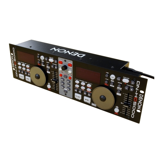
DN-HC5000
Serato ITCH
for Mobile Entertainers
TM
For purposes of improvement, specifications and design are subject to change without notice.
●
Please use this service manual with referring to the operating instructions without fail.
●
Some illustrations using in this service manual are slightly different from the actual set.
●
X0458V01DM/DG0910
Copyright 2009 D&M Holdings Inc. All rights reserved.
WARNING: Violators will be prosecuted to the maximum extent possible.
Advertisement

Related Manuals for Denon DN-HC5000


Summary of Contents for Denon DN-HC5000
- Page 1 Ver. 1 SERVICE MANUAL MODEL E2A E2C E1K EUT DN-HC5000 Serato ITCH for Mobile Entertainers For purposes of improvement, specifications and design are subject to change without notice. ● Please use this service manual with referring to the operating instructions without fail.
-
Page 2: Safety Precautions
SAFETY PRECAUTIONS The following check should be performed for the continued protection of the customer and service technician. LEAKAGE CURRENT CHECK Before returning the unit to the customer, make sure you make either (1) a leakage current check or (2) a line to chassis resistance check. - Page 3 DIMENSION...
- Page 4 WIRE ARRANGEMENT If wire bundles are untied or moved to perform adjustment or parts replacement etc., be sure to rearrange them neatly as they were originally bundled or placed afterward. Otherwise, incorrect arrangement can be a cause of noise generation. ※Refer to 6~8 page for folding the FFC.
- Page 5 (4) Fasten the two 4P connectors with a cord holder. •Fasten the cord not to touch the trans. CX271 CX272 CX041 CX042 (5) It coverd with TOP PANEL SUB ASSY. NOTE:The wire gets caught in TOP PANEL SUB ASSY.
- Page 6 Folding the FFC (1) 8U-110066-1 PANEL1 UNIT (00D0090290040 : 27P FFC(1.0) L=400) 160mm 45mm 55mm White surface Printed surface Fold as shown on the diagram. Fold as shown on the diagram. Fold inward 35mm 35mm Fold outward Fold inward...
- Page 7 (2) 8U-110066-2 PANEL2 UNIT (00D0090290053 : 27P FFC(1.0) L=200 ) 65mm 25mm Fold outward Fold outward Fold inward Fold inward 45mm Fold outward Fold as shown on the diagram. Fold as shown on the diagram.
- Page 8 (3) 8U-110066-5 DISC1 UNIT / 8U-110066-6 DISC2 UNIT (00D0090290037 : 11P FFC(1.0) L=60) 16mm Fold inward Place fold against the A side. Fold outward Fold inward 16mm Fold as shown on the diagram.
- Page 9 DISASSEMBLY (Follow the procedure below in reverse order when reassembling.) 1. Top Panel Unit (1) Remove 10 side screws with washer and pull up the Top Panel Unit. Notes: Do not pull out aslant to prevent FFC cable damage. Do not fail to pull AC cord from wall outlet before disconnect the FFC cable and wire. If AC cord is remained plugged into wall outlet, power is kept supplied in the unit, which may cause damage.
- Page 10 ASSEMBLY NOTE Mounting the JOG DISC (1) Mount SLIP MAT (B) on the JOG WHEEL SUB ASSY. SLIP MAT (B) : Ref No. 34 (The slip mat has no specific front or rear side.) JOG WHEEL SUB ASSY : Ref No. 38 (2) Next mount SLIP MAT.
- Page 11 SERVICE MODE 1. Turning on the power in the service mode (1) Turn on the power while pressing the PARAMETERS knob and the NEXT button (Deck 1 or Deck 2) simultaneously. The following appears on the VFD segment display section: (2) When the PARAMETERS knob is turned clockwise, the display on the lower tier of the VFD segment display section switches in the following order: "Function CHK"...
- Page 12 3. Service mode function table Mode Summary Remark Turn on the power while pressing the PARAMETERS knob and the To cancel the service Service Mode TOP NEXT button (Deck 1 or Deck 2) simultaneously. mode, turn the power (Service Mode) off.
- Page 13 Mode Summary Remark ※ Display of the status and results of the various control elements on the panel surface and external input from the side panel • PARAMETERS knob The segment on the right side of the "P" column at the upper left of the VFD segment display section toggles between white and black each time the PARAMETERS knob is pressed.
- Page 14 3.1. Switch check mode (SW Check) (1) All the VFD characters are turned off. The following characters are assigned to the 12 places of the VFD segment display section: (2) When each switch is pushed → Turn on the pertinent figure in the third place of the track number. →...
- Page 15 3.2. Touch measurement mode(Touch MEAS) (1) All the VFD characters are turned off. The following appears on the VFD segment display section:(Count value display mode) *** : Current touch count value is displayed. (TP : TOP, BM : BOTTOM, RT : RIGHT, LT : LEFT) The average of the count values acquired for the first four times measurements are made after this mode is set is calculated and used as the reference value.
- Page 16 3.3. MIDI COMMANDS (1) Data transmission The panel operation data is transmitted by MIDI command, as per the table below. Send command to PC ● MIDI command items Message type Command Number Value SW ON : 0x9n SW ON : 0x40 Playlist 0x02 Note ON/OFF...
- Page 17 A1 Dimmer 0x3C 0x25 A2 Dimmer 0x3D 0x26 Play 0x27 Jogwheel 0x3B only Use 0x4A DN-HC5000 return Pitch slider request 0x3C (request TRG) pitch slider position only Use 0x4A DN-HC5000 return X-Control fader request 0x3D (request TRG) XControl fader position...
- Page 18 VFD symbol data reception The Various Vfd Symbols Can Be Set To On, Off Or Blinking, As Per The Table Below. Receive command for VFD Symbol ● MIDI command items Message type Command Number Value ON TRG : 0x4D VFD Symbol 0xBn OFF TRG : 0x4E Control Change...
- Page 19 MIDI command items Message type Command Number Value ON TRG : 0x4D VFD Symbol 0xBn OFF TRG : 0x4E Control Change ↓ Blink ON TRG : 0x4F 0x2C Scratch Position 11 only Use 0x4D/0x4E 0x2D Scratch Position 12 only Use 0x4D/0x4E 0x2E Scratch Position 13 only Use 0x4D/0x4E...
- Page 20 VFD parameter data reception The time-related display and segment display can be set by MIDI command, as per the table below. Receive command for VFD Parameter ● MIDI command Items Message Type Command Number Value VFD Parameter 0-99 Tr number MSB 0xBn 0x40 100-109 : “-0”...
- Page 21 Segment 2-5 MSB 0x12 ↑ ↑ ↑ Segment 2-6 MSB 0x13 ↑ ↑ ↑ Segment 2-7 MSB 0x14 ↑ ↑ ↑ Segment 2-8 MSB 0x15 ↑ ↑ ↑ Segment 2-9 MSB 0x16 ↑ ↑ ↑ Segment 2-10 MSB 0x17 ↑ ↑...
- Page 22 VFD segment data reception The various segments are set by 2-byte data, as per the following font code. (0x00/0x00 to 0x00/0x07 cannot be used.) Font codes for segments ● ※ For the Reflex function operations corresponding to the above MIDI commands, refer to the Reflex manual.
- Page 23 If the device is not yet connected, the following appears on the VFD segment display section: D i s c o n n . . on Deck2 (2) Launch the DN-HC5000 update program. The screen shown below appears on thecomputer. Current version information...
- Page 24 If the update file has not been loaded, “Fileis not ready.” is displayed. The device is not in the update mode. (4) Drag and drop the update file to the ”DENON DJ Upgrade program” screen. The Load button can now be selected.
- Page 25 (5) Press the Load button to transfer the update file. (6) The following appears on the VFD segment display section: During file transfer:on Deck1 U p d a t e M o d e L o a d i n g Once file transfer is finished;...
- Page 26 (8) Press the OK button to finish. The following appears on the VFD segment display section: On Deck2: L i n k e d P o w e r O f f ! ! Quit the updating program and turn off the DN-HC5000’s power.
- Page 27 NOTE: • Do not turn off the set’s power or disconnect the cable connecting it to the computer during loading or version updating. Also, do not press any buttons on the set or any keys on the computer’s keyboard. • If an error message appears during loading or version updating, repeat from step 1. Other error messages are as follows: “File is invalid”...
-
Page 28: Trouble Shooting
TROUBLE SHOOTING FLOW CHART NO.1 The power cannot be turned on. Is the fuse normal? See FLOW CHART No.2 <The fuse blows out.> Is normal state restored when once unplugged Check if there is any leak or short-circuiting on the power cord is plugged again after several seconds? primary circuit component, and replace it if defective. - Page 29 FLOW CHART NO.7 -8V is not outputted. Check D903, D904 and the periphery circuit, Is the voltage of -10V or less supplied to INPUTpin and replace it if defective. of IC905? Check IC905 and the periphery circuit, and replace it if defective. FLOW CHART NO.8 +5VA is not outputted.
- Page 30 FLOW CHART NO.12 The key operation is not functioning. Are the contact point and the installation state of the Re-install the switches (S701~734, S801~830) key switches (S701~734, S801~830) normal? correctly or replace the poor switch. Check the TR701~708(TR807~814)and Does LED(LD701~739, LD801~829) light correctly ? their periphery, and service it if detective.
-
Page 31: Level Diagram
LEVEL DIAGRAM OUTPUT Audio SH7263 PCM178 +6.0dBV +2.78dBV 0dBFS GAIN=3.22dB GAIN=2.78dB -92dBV -95.22dBV 16bit:SNR=98dB -100dBV -100 -103.22dBV PCM1781:SNR=106dB(typ) -120 -130 -140 -150... - Page 32 SEMICONDUCTORS Only major semiconductors are shown, general semiconductors etc. are omitted to list. 1. IC’s R5S72630P200FP (IC104)
- Page 33 R5S72630P200FP Block Diagram...
- Page 34 R5S72630P200FP Terminal Function Pin No. Pin Name Symbol Function PC10/-RASU /MUTE General-purpose port Not used: OPEN -CASL SHCAS %CASL% SDRAM /CAS -RASL SHRAS %RASL% SDRAM /RAS V1SH Power supply for in Digital +1.2V DQMUU DQMUU Not used: OPEN DGND Digital GND PVSS DGND GND for I/O...
- Page 35 Pin No. Pin Name Symbol Function -CS4 Not used: OPEN PE4/DREQ0 General-purpose port Not used: OPEN PVSS DGND GND for I/O Digital GND PE5/DACK0 DRVDET DRVDET input Terminal Drive connection detection signal PVCC V3SH Power supply for I/O Digital +3.3V PE6/RXD2 Terminal Drive PE7/TXD2...
- Page 36 Pin No. Pin Name Symbol Function PVCC V3SH Power supply for I/O Digital +3.3V SSIDATA3 DATA_A Audio data For Deck1 SSIWS3 LRCK Audio word clock For Deck1 SSISCK3 Audio BCK For Deck1 V1SH Power supply for in Digital +1.2V AUDIO_CLK AUDIO_CLK Master clock for audio Change input of 16.9344MHz/24.576MHz on the outside...
- Page 37 Pin No. Pin Name Symbol Function PB4/SCL2 General-purpose port Not used: 3.3k pull-up PB5/SDA2 General-purpose port Not used: 3.3k pull-up PVSS DGND GND for I/O Digital GND DGND Digital GND PB6/SCL3 KEYDAT2 KEYDAT2 Deck2 SW/ENC data input PB7/SDA3 KEYDAT1 KEYDAT1 Deck1 SW/ENC data input V1SH Power supply for in...
- Page 38 W981616BH-7 (IC102) PIN DESCRIPTION PIN NUMBER PIN NAME FUNCTION DESCRIPTION 20- 24, DQ15 Address Multiplexed pins for row and column address. A0- A10 27- 32 Row address: A0- A10. Column address: A0- A7. DQ14 Bank Select Select bank to activate during row address latch time, or bank to read/write during column address latch DQ13 time.
- Page 39 B6TS-04LT (IC706, 803) TB62777FNG (IC704, 805) PCM1781 (IC802, 803) OUT2/SCK OUT1/SCS ZEROA OUT3/SD OUT0/CHG 2 DEMP0 SERIAL-IN R-EXT RESET CH0A CLOCK SERIAL-OUT 3 DEMP1 TEST1 CH0B LATCH ENABLE 4 MUTE OUT0 OUT7 MEAS CH1A 5 SCK AGND CH1B OUT1 OUT6 6 DATA TEST2 CH2A...
- Page 40 2. VFD MODULE 17-BT-30GINK CGROM code table...
-
Page 41: Block Diagram
BLOCK DIAGRAM DN-HC5000 block Diagram GND0 +3.3V AC Sel Main Power Main Power +1.2V +1.2V Jumper +1.2V DC-DC CY081 CW081 8PMINI SH7263 DND REMOTE DC-DC 16.9344MHz TRANS AC SW /25.476MHz CX141 USB Device Audio MCLK +3.3V (MIDI/HID/Speaker) 14pin Operation cont... - Page 42 PRINTED WIRING BOARDS GU-3849 MAIN P.W.B. UNIT FOIL SIDE COMPONENT SIDE...
- Page 43 GU-3850A POWER P.W.B. UNIT COMPONENT SIDE FOIL SIDE...
- Page 44 8U-110066 PANEL P.W.B. UNIT (1/2) COMPONENT SIDE...
- Page 45 8U-110066 PANEL P.W.B. UNIT (2/2) FOIL SIDE...
-
Page 46: Wiring Diagram
WIRING DIAGRAM CW041 CX041 or CX042 CX112 CY271 CX271 CY112 or CY113 CH3 DOWN 11 1 CH3A 1 SC0 CH2 RIGHT 9 3 CH2A 3 SC2 DGND 1 DGND DGND_5 6 DGND BLINK 6 BLINK DATA1 4 DATA1 CH1 UP 9 CH1A 9 +5V 7 BCK... - Page 47 NOTE FOR PARTS LIST Parts for which "nsp" is indicated on this table cannot be supplied. When ordering of part, clearly indicate "1" and "I" (i) to avoid mis-supplying. Ordering part without stating its part number can not be supplied. Part indicated with the mark "★"...
- Page 48 PARTS LIST OF P.W.B. UNIT * Parts for which "nsp" is indicated on this table cannot be supplied. * The parts listed below are for maintenance only, might differ from the parts used in the unit in appearances or dimensions. Note: The symbols in the column "Remarks"...
- Page 49 Ref. No. Part No. Part Name Remarks Q'ty CAPACITORS GROUP C101 CK73F1E104ZT +1608 C102 CK73B1H103KT (1608) +1608 C103 CK73B1E104KT +1608 C104 CC73CH1H470JT +1608 C105 CK73B1E104KT +1608 C106 CK73B1H103KT (1608) +1608 C107 CK73F1E104ZT +1608 C108,109 CK73B1E104KT +1608 C110,111 CK73B1H103KT (1608) +1608 C112 CK73F1E104ZT +1608...
- Page 50 Ref. No. Part No. Part Name Remarks Q'ty C405 CK73B1E104KT +1608 C406 00D2544655906 CE67C0J220MT (RV2) +REF C407 CK73B1E104KT +1608 C408 00D2544656934 CE67C1A470MT (RV2) C409 CK73B1H103KT (1608) +1608 C410-412 00D2570038908 CK73B1A106KT +2125 C413 CK73B1A474KT C414 CK73F1E104ZT +1608 C415 CK73B1E223KT +1608 C418-423 CK73F1E104ZT +1608 C424...
- Page 51 GU-3850AE3 POWER UNIT P.W.B. ASSY(E3 model) GU-3850AE2 POWER UNIT P.W.B. ASSY(E2 model) Ref. No. Part No. Part Name Remarks Q'ty SEMICONDUCTORS GROUP IC801 00D2630809006 NJM7805FA(S) IC802,803 00D2623692903 PCM1781 IC804,805 00D2630896909 NJM2068MD-TE1 IC901 00D2623765005 BD9703T-V5 IC902 00D2623698004 BA33BC0WT-V5 IC903 00D2630454901 M51957BFP(TP1) IC904 00D2630810008 NJM7808FA(S)
- Page 52 Ref. No. Part No. Part Name Remarks Q'ty C847 CK73B1E104KT +1608 C848 CK73B1H103KT (1608) +1608 C901 RM73B--0R0KT +1608 C902 CK73F1H103ZT +1608 C903 00D2538022707 CK45F2EAC103MC C904 RM73B--0R0KT +1608 C905 CK73F1H103ZT +1608 C906 00D2544536915 CE04W1A470MT SMG/RE3 C907-911 CK73B1E104KT +1608 C912,913 00D2538029713 CK45F2EAC471KC(KX) C914 00D2568038004 CF99--2EAC104M...
- Page 53 Ref. No. Part No. Part Name Remarks Q'ty S901 665010008002D POWER SWITCH (TV-5) T901 00D2336608006 POWER TRANS W901 M3 SCREW TERMINAL RB901 00MHV00033020 #ERZV07D471...
- Page 54 8U-110066 PANEL UNIT P.W.B. ASSY Ref. No. Part No. Part Name Remarks Q'ty SEMICONDUCTORS GROUP IC701 00D2622953915 SN74HCT138APW IC702 00D2623694901 SN74LV165APW IC703 00D2690226001 GP1A038RBK IC704 235710040507P TB62777FNG IC705 00D2622557900 SN74LV14APW-EL2 +REF IC706 00D2623691904 B6TS-04LT IC801 00D2690226001 GP1A038RBK IC802 00D2623694901 SN74LV165APW IC803 00D2623691904 B6TS-04LT...
- Page 55 Ref. No. Part No. Part Name Remarks Q'ty LD803 00D3939606909 SEL6927A(TP5) LD804 00D3939660903 SELU5223C-S(RED) LD805,806 00D3939606909 SEL6927A(TP5) LD807,808 00D3939674902 SLR343EC4TT32 LD809-811 00D3939606909 SEL6927A(TP5) LD812,813 00D3939608907 SLR342MC(TB7) LD814 00D3939605900 SEL6427EP(TP5) LD815,816 00D3939606909 SEL6927A(TP5) LD817 00D3939607908 SLR342VC(TB7) LD818 00D3939606909 SEL6927A(TP5) LD819 00D3939605900 SEL6427EP(TP5) LD820,821 00D3939675901...
- Page 56 Ref. No. Part No. Part Name Remarks Q'ty C816-818 CK73F1E104ZT +1608 C819,820 CK73F1H103ZT +1608 C821 00D2544302974 CE04W1A101MT(SRE) C822,823 CK73F1E104ZT +1608 C826 00D2544300918 CE04W0J100MT(SRE) C827,828 CK73F1E104ZT +1608 C829 00D2570504911 CC73CH1H240JT C830,831 CK73F1E104ZT +1608 C832-834 00D2570504911 CC73CH1H240JT C835-838 CK73B1E104KT +1608 C842 CK73F1E104ZT +1608 C843 00D2544300918...
- Page 57 EXPLODED VIEW 106 105 WARNING: Parts marked with this symbol have critical characteristics. Use ONLY replacement parts recommended by the manufacturer.
- Page 58 ---MEMO---...
- Page 59 PARTS LIST OF EXPLODED VIEW * Parts for which "nsp" is indicated on this table cannot be supplied. * P.W.B. ASS'Y for which "nsp" is indicated on this table cannot be supplied. When repairing the P.W.B. ASS'Y, check the board parts table and order replacement parts. *...
- Page 60 Ref. No. Part No. Part Name Remarks Q'ty 00D1132078103 SLIDE KNOB 00D1121024100 KNOB 00D4611304007 BUFFER R. SHEET E3 SUB ASSY ★ 46 R. SHEET E2 SUB ASSY ★ 46 C-UL MARK US ★ 47 FCC/CLASS B CAUTION ★ 48 SCREWS 0RD4737505010 2.6X6 CBTS (P)-Z 0RD4737002034...
- Page 61 PACKING VIEW PARTS LIST OF PACKING & ACCESSORIES * Parts for which "nsp" is indicated on this table cannot be supplied. * The parts listed below are for maintenance only, might differ from the parts used in the unit in appearances or dimensions. Note: The symbols in the column "Remarks"...
- Page 62 NOTE FOR SCHEMATIC DIAGRAM WARNING: Parts marked with this symbol z have critical characteristics. Use ONLY replacement parts recommended by the manufacturer. CAUTION: Before returning the unit to the customer, make sure you make either (1) a leakage current check or (2) a line to chassis resistance check.
- Page 63 SCHEMATIC DIAGRAMS (1/5) 8U-110066-1 PANEL1 UNIT 8U-110066-3 SENSOR1 UNIT 8U-110066-5 DISC1 UNIT DN-HC5000...
- Page 64 SCHEMATIC DIAGRAMS (2/5) 8U-110066-2 PANEL2 UNIT 8U-110066-4 SENSOR2 UNIT 8U-110066-6 DISC2 UNIT DN-HC5000...
- Page 65 SIGNAL LINE SCHEMATIC DIAGRAMS (3/5) GU-3849 MAIN UNIT (1/2) DN-HC5000...
- Page 66 SCHEMATIC DIAGRAMS (4/5) GU-3849 MAIN UNIT (2/2) DN-HC5000...
- Page 67 SIGNAL LINE SCHEMATIC DIAGRAMS (5/5) GU-3850A POWER UNIT DN-HC5000...