Table of Contents
Advertisement
Blue-Ray Disc Player
C
o
n
e t
n
s t
...................................................1-1 to 1-10
2 Laser Beam Safety Precautions......................................... 2-1
3 Important Safety Precautions .................................. 3-1 to 3-2
4 Safety Check After Servicing ............................................. 4-1
Requirements .................................................................... 5-1
7 Direction of Use ....................................................... 7-1 to 7-6
8 Cabinet Disassembly Instructions ........................... 8-1 to 8-2
9 Troubleshooting ....................................................... 9-1 to 9-2
10 Block Diagram .................................................................10-1
11 Wiring Diagram ...............................................................11-1
12 Headphone & MP3 Link and USB、LED Board
Circuit Diagram ....................................................12-1
Layout Diagram ...................................................12-1
13 AMP Board
Circuit Diagram ....................................................12-2
Layout Diagram ...................................................12-3
© Copyright 2011 Philips Consumer Electronics B.V. Eindhoven, The Netherlands.
All rights reserved. No part of this publication may be reproduced, stored in a
retrieval system or transmitted, in any form or by any means, electronic,
mechanical, photocopying, or otherwise without the prior permission of Philips.
Published by Sophie-KM 1123 AVM
Version 1.0
P
a
g
e
Contents
14 Display Board
15 Key Board
16 Power Board
17 Decoder Board
18 Exploded View....................................................................13-1
19 Revision List .......................................................................14-1
Printed in the Netherlands
MBD7020/12/93
Circuit Diagram ................................................12-4
Layout Diagram ...............................................12-5
Circuit Diagram .................................................12-6
Layout Diagram.................................................12-7
Circuit Diagram ........................................12-8 to 12-9
Layout Diagram ..............................................12-10
Circuit Diagram .................................12-11 to 12-19
Layout Diagram ..............................................12-20
Feature
Different
Features
RDS
Voltage Selector
ECO Standby
DTS
Subject to modi cation
Page
/12 /93
EN
3141 785 36200
Advertisement
Table of Contents

Related Manuals for Philips MBD7020/12


Summary of Contents for Philips MBD7020/12
-
Page 1: Table Of Contents
Different /12 /93 Features © Copyright 2011 Philips Consumer Electronics B.V. Eindhoven, The Netherlands. All rights reserved. No part of this publication may be reproduced, stored in a Voltage Selector retrieval system or transmitted, in any form or by any means, electronic, ECO Standby mechanical, photocopying, or otherwise without the prior permission of Philips. -
Page 2: Technical Specification And Connection Facilities
Technical Specification and Connection Facilities Location of PC Boards Decoder Board AMP Board Bl-Ray Loader Key Board USB Board Power Board Headphone/MP3 Link Board LED Board Display Board Version Variations Type /Versions: MBD7020 Service policy Board in used: LED Board Decoder Board Display Board AMP Board... - Page 3 Technical Specification and Connection Facilities Technical Specification 2 General Specification Product family features 2.1.1 Styling and functions MBD7020 appearances are defined In MUS. MUS is the leading document where product appearance is applicable. MBD7020 Features Products [ALL Stroke Version] s l i Dimension W x D x H (mm) [250x93.5 x286]mm...
- Page 4 Technical Specification and Connection Facilities MBD7020 Interface Type [All Stroke Version] USB Type A Receptacle [Color: Black] 2.1.3 Product Controls MBD7020 Remark Controls / Indicators [ALL Stroke Version] Buttons Rotary Fade-on and Fade-off effect is required. Volume Knob [with white Led] Refer to UIS for LED detailed behavior Light cast downward ,bright at the centre and fades towards the sides...
- Page 5 Technical Specification and Connection Facilities 3.2 Climatic Tests 3.2.1 Exposure Test (Non-Operating) 3.2.2 Functional Test (Operating) 4 Performance Specifications 4.1 Audio Performance 4.1.1 Reference levels Audio inputs Audio Outputs Audio Input Sensitivity (±3dB) rated output power at 1KHz Audio Output(*1) Tuner FM 67.5KHz,Modulation (Limit:-6dB) Line Out (Left/Right)
- Page 6 Technical Specification and Connection Facilities 4.1.2 Amplifier Output Measurements are done with rated speaker impedance. Description Specification Rated Output Power @ 10%THD 50W± 0.5dB Channel Unbalance(1KHz) |2.0|dB Crosstalk (20Hz – 20KHz) |50|dB Frequency Response (30Hz – 16KHz ) ± 3dB Frequency Response with De-emphasis +0.5 / -2.0dB ( 20Hz –...
- Page 7 Technical Specification and Connection Facilities 4.1.5 Digital Audio Outputs Standard Reference IEC 60958 IEC 61937 4.1.5.1 Coaxial & Optical Output Required to support up to bitrate of up to 96KHz SPDIF input. Description Specification Test Condition Output signal amplitude 0.5 Vpp ± 20% termination Output impedance ±...
- Page 8 Technical Specification and Connection Facilities 4.2.2 Component Video (Y/Pb/Pr) Description Test Signal Specification Interlace/Progressive NTSC i l p ± ± ± ± PbPr peak to peak 75% Color bar 525mV ± 10% 535mV ± 10% 75% Color bar PbPr Output unbalance i l p ±...
- Page 9 Technical Specification and Connection Facilities 4.3.2 1080i Component Video (Y/Pb/Pr) Test Picture Parameter Specification Y White Level 700mV± 10% Sync Amplitude Positive Pary 300mV± 10% Sync Amplitude Negative Part 100% White 300mV± 10% Y Amplitude O/P 1000mV± 10% S/N Y 60dB DC Level Y(Blanking Level) DC Level P...
- Page 10 Technical Specification and Connection Facilities TEST ITEMS UNIT NOM. LIMIT 87.5 Frequency Range 90MHz 24~30 19~35 TUNING SENS 98MHz 24~30 19~35 106MHz 24~30 19~35 -3dB LIMITING POINT 26dB QUENTING SENSITIVITY FM IF REJEDION 98MHZ S/N=26dB IMAGE REJECT 98MHZ S/N=26dB 300kHz SELECTIVITYS >500KHz TUNING ACCURAY...
- Page 11 Technical Specification and Connection Facilities 4.7 HDMI Standard Reference High-Definition Multimedia Interface Specification version 1.3a High-Definition Multimedia Interface Compliance Test Specification version 1.4 4.7.1 Standard Reference: USB specification Revision 2.0,dated 27 April 2000 USB-IF USB 2.0 Electrical Test Specification Version1.03, dated January 2005 USB-IF Embedded Host Compliance Plan , Revision 1.0, dated August 2006 USB 1A requirement 4.8 Ethernet...
-
Page 12: Laser Beam Safety Precautions
Laser Beam Safety Precautions This Blu-Ray player uses a pickup that emits a laser beam. Do not look directly at the laser beam coming from the pickup or allow it to strike against your skin. The laser beam is emitted from the location shown in the figure. When checking the laser diode, be sure to keep your eyes at least 30 cm away from the pickup lens when the diode is turned on. -
Page 13: Important Safety Precautions
Remove discs from the disc compartment and the wall mount. Koninklijke Philips if you are not using the product for an Electronics N.V. bears no responsibility extended period of time. - Page 14 Important Safety Precautions Disposal of your old product and batteries Your product is designed and manufactured with high quality materials and components, which can be recycled and reused. When this crossed-out wheeled bin symbol is attached to a product it means that the product is covered by the European Directive 2002/96/EC.
-
Page 15: Safety Check After Servicing
Safety Check after Servicing Examine the area surrounding the repaired location for damage or deterioration. Observe that screws, parts, and wires have been returned to their original positions. Afterwards, do the following tests and confirm the specified values to verify compliance with safety standards. 1. -
Page 16: Safety Information General Notes & Lead Free Requirements
Safety Information, General Notes & Lead Free Requirements Safety Instructions Warnings General Safety General Safety regulations require that during a repair: All ICs and many other semiconductors are susceptible to Connect the unit to the mains via an isolation transformer. electrostatic discharges (ESD, ). -
Page 17: Standard Notes For Servicing,Lead Free Requirements & Handling Flat Pack Ic
1. The output pin of the 3 pin Regulator ICs is When soldering, be sure to use the Pb free solder. indicated as shown. Information about lead-free soldering Top View Philips CE is producing lead-free sets from 1.1.2005 Bottom View onwards. Input IDENTIFICATION Regardless of special logo (not always 2. - Page 18 2004), containing leaded solder-alloy and components, all needed spare-parts will be available till the end of the service-period. For repair of such sets nothing changes. On our website www.atyourservice.ce.Philips.com you find more Fig. S-1-1 information to: BGA-de-/soldering (+ baking instructions) 2.
- Page 19 Standard Notes for Servicing, Lead Free Requirements & Handling Flat Pack IC 3. The flat pack-IC on the CBA is affixed with glue, so 4. Release the flat pack-IC from the CBA using be careful not to break or damage the foil of each tweezers.
- Page 20 Standard Notes for Servicing, Lead Free Requirements & Handling Flat Pack IC Instructions for Handling Semi- 2. Installation conductors 1. Using desoldering braid, remove the solder from the foil of each pin of the flat pack-IC on the CBA Electrostatic breakdown of the semi-conductors may so you can install a replacement flat pack-IC more occur due to a potential difference caused by easily.
-
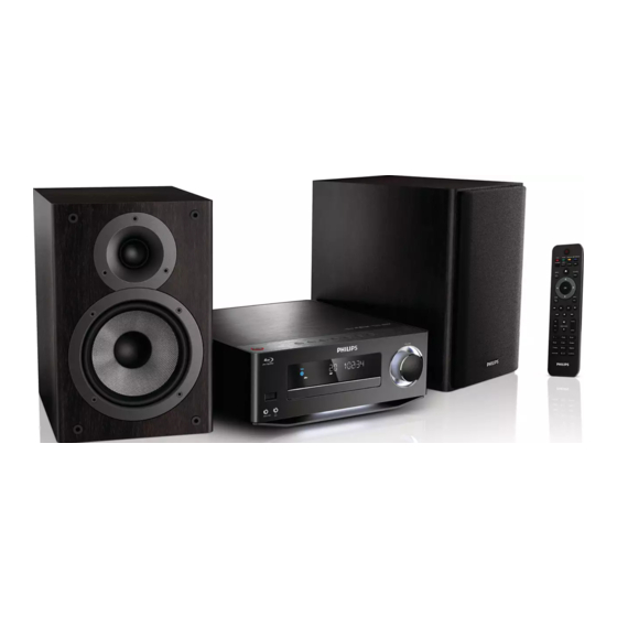
Page 21: Direction Of Use
The following excerpt of the DFU/QSG serves as an introduction to the set. The Complete Direction for Use can be download in different languages from the internet site of Philips Customer care Center : www.support.philips.com IR sensor Overview of the main unit Detect signals from the remote control. - Page 22 Direction of Use Remote Control LOUDNESS Turn on or off automatic loudness adjustment. Turn on this product or switch to Eco Power standby mode. PROGRAM When EasyLink is enabled,press Program radio stations. and hold for at least three seconds OPEN/CLOSE to turn all connected HDMI CEC Open or close the disc compliant devices to standby.
- Page 23 Direction of Use 3 Connect Connect speakers Note Make the following connections to use this product. Insert the stripped portion of each speaker wire into the socket completely. For optimal sound,use the supplied speakers only. Connect only speakers with impedance that is the Preparations same or higher than the supplied speakers.
- Page 24 Direction of Use Insert fully the silver end of the speaker Connect a composite video cable to: cableinto the black(-) connector. the VIDEOjack on this product. the VIDEO input jack on the TV. Screwthe black(-) connectorto secure the cable. Connect the audio cables to: the LINE OUT/AUDIO -L/Rjacks Repeat steps 2-6 for the right speaker on this product.
- Page 25 Direction of Use Connect to a digital AV ampli er/ receiver LINEOUT COAXIAL LINE OUT AU X IN DIGITAL OUT LINE OUT AU X IN COAXIAL AUX IN Connecta coaxial c able(not supplied) to: the COAXIAL jack on this product. Press MP3 LINK/AUX to select the audio the COAXIAL/DIGITAL input jack output of your connection.
-
Page 26: Connect A Network
LINE OUT AU X IN Note DOCK Internet access to Philips website for software update may not be allowed,depending on the router you use or the Internet Service Provider’s policy. Contact your Internet Service Provider for more information. Connect a dock(not supplied) to the Connect power DOCK socket on this unit. -
Page 27: Cabinet Disassembly Instructions
Cabinet Disassembly Instructions Note: 1. Disassembly Flowchart (1) Identification (location) No. of parts in the figures This flowchart indicates the disassembly steps to gain (2) Name of the part access to item(s) to be serviced. When reassembling, (3) Figure Number for reference follow the steps in reverse order. - Page 28 Cabinet Disassembly Instructions A010 Fig. D3 Fig. D6 Fig. D4 Fig. D7 A011 A012 Fig. D5 Fig. D8...
-
Page 29: Troubleshooting
Troubleshooting FLOW CHART NO.1 NO Power(The power cannot be turned on) Check the Power Cable connect is ok or not Check and Change the connect cable TEST Power supply voltage output CON4 each TEST CON4 “ECO”pin whether plate is normal or not(+12V\DC5V\MCU\5V\P25V) has high level signal Check the fuse which location F1 replace a new one... - Page 30 Troubleshooting FLOW CHART NO.3 VFD no display Check VFD display board CN301 whether connection to decoder board CN1 is normal Check VFD display board CN401 whether Test whether VFD board CN401 pin 12#~13# between connection to KEYS board CN301 is normal has AC5V provide voltage Check the KEYS board location Check whether VFD board U401 pin 14#\33#\45# has +V5 B301 related electric circuit...
-
Page 31: Block Diagram
Block Diagram CONTROL BY MCU WIFI DONGLE MODULE 5V 0.5A BRAND: ALPHA USB0 REAR WIFI DONGLE CONTROL BY BD TRV414H05 (Atheros AR9271) Model Number: WUS-N11 Power Switch TPS2553DBVT Collimator II TPC1391G4 ??K 1% resistor BD TRAVERSE Ethernet RJ45 A DDRIII X 1 U V W COM AABBUVWC Motor Driver... -
Page 32: Wiring Diagram
Wiring Diagram LINE OUT M-BOY DIN9 1.0/4P IPOD DET SGND 2.5/4P 2.0/4P AGND 2.0/8P 2.0/7P ACC_DET 4705 2.5/2P CS5346 PS9831 TAS5342 R5F21258 DRV604 2.0/4P 1.0/10P 2.5/9P 2.5/2P OPTICAL CVBS COAXIAL USB WIFI HDMI ready 2.0/5P 1.0/8P 2.0/5P 2.0/4P 1.0/12P 2.5/6P 2.5/2P 2.0/4P 1.0/8P... -
Page 34: Circuit Diagram
Amp Board -- Circuit Diagram FM_CP_RST DAB_MUTE R193 NC/330 ipod/DAB_TX R169 R170 R194 NC/330 ipod/DAB_RX FB600 NC/0 P25V +12V /RST A5V MCU_5V SCL3 R175 330/NC FB/600 MSCL R179 0R/NC/NC SDA3 R173 330/NC FB/600 MSDA FM5V FM5V FB/600 TO MCU + CE1 FB/1K FM_INR R180... -
Page 35: Layout Diagram
AMP Board -- Layout Diagram 12-3 12-3... -
Page 40: Circuit Diagram
Power Board -- Circuit Diagram 1 COLD +12V 22R 1206 102P 400V 3.3uH 5x7mm 1nF,200V Q5 B772 22R 1206 47R 1206 9.1K 1% 0805 3.3K 0805 ER28 100P 0805 103P/630V 103P/1KV 33uF/35V SB3100 3.3K 0805 62K/1W 100uF 25V FB,120R,8A MMBT2222 1000uF/25V 3.6V 5% Ferrite Bead,120R,4A... - Page 41 Power Board -- Circuit Diagram 2 JMP5 GBL406 NTC,MF72,5D-11 T5AH250V T18*10*7,0.45*45Ts,20MH T18*10*7,0.45*45Ts,20MH JUMP 5mm 47uF/400V JMP1 NC CON4 10D471K T6.3AH250V 10D561K 47uF/400V JUMP 5mm 22uF/400V 14D561K HGND COLD 1K 0805 PC817 MMBT2222 33V 5% R58 1K 0805 100R 1206 1K 0805 U2_V FR107 100R 1206...
-
Page 42: Layout Diagram
Power Board -- Layout Diagram 12-10 12-10... -
Page 43: Circuit Diagram
Decoder Board -- Circuit Diagram 1 VCC_P FB4 BLM21P 12V_P VCC_P 0.1uF/10V BEAD/SMD/0805 CE307 0.1uF/10V 10uF/10V/X5R NC0805/SMD C0805/SMD P1_GND 100uF R12 10 VCC_1.1V 10uF/10V/X5R L0805B 1.1V 10uF/16V/X5R 10uF/10V/X5R 0.1uF/10V/X5R C0805/SMD 2.2uH/LQH6PPN2R2N43 C0805/SMD C0805/SMD FB904 R3 2.4K 1.1V_EN FB601/5A L0805B L0805B 1.1V_FB 10/NC CB16... - Page 44 Decoder Board -- Circuit Diagram 2 U100A MT8550-DDR3-BGA492-090924 1.5V A_DQ0 A_RA0 1.5V A_DQ7 A_RA1 A_DQ1 A_RA2 C142 C118 A_DQ6 A_RA3 0.01uF/6.3V/X5R 0.1uF/6.3V/X5R CE100 A_DQ3 A_RA4 AB20 DVCC18_IO_1 220uF/16V AB21 A_DQ5 A_RA5 DVCC18_IO_1 A_DQ0 A_DQ2 A_RA6 AC10 AE16 DVCC18_IO_1 RDQ0 A_DQ1 A_DQ4 A_RA7 AC13...
- Page 45 Decoder Board -- Circuit Diagram 3 U100B MT8550-DDR3-BGA492-090924 U203 1.1V IC DDR3 x16 FBGA-96 B_DQ0 B_RA0 1.1V B_DQ6 B_RA1 C207 C206 B_DQ3 B_RA2 CE205 0.01uF/6.3V/X5R 0.1uF/6.3V/X5R B_DQ5 B_RA3 DVCC10_K 470uF/10V B_DQ1 B_RA4 DVCC10_K B_DQ0 B_DQ4 B_RA5 DVCC10_K RDQ0_B B_DQ1 B_DQ2 B_RA6 DVCC10_K RDQ1_B...
- Page 46 Decoder Board -- Circuit Diagram 4 U100C 3.3V 1.2V R343 AUDIO I2S AVDD33_VDACY AVDD12_HDMI R350 AOSDATA5 C304 C303 AOSDATA5 C300 C313 AOSDATA4 AOSDATA4 0.1uF/6.3V 10uF/6.3V/X5R 0.1uF/6.3V AOSDATA3 C0603/SMD AOSDATA3 AOSDATA2 AVDD33_VDACR AOMCLK_R C0805/SMD AOSDATA2 AVDD33_VDAC_R AOMCLK TP310 AOSDATA1 AOBCK_R AOSDATA1 AVSS33_VDAC_R AOBCK TP311...
- Page 47 Decoder Board -- Circuit Diagram 5 HW TRAPPING NFWEN NFWEN U100E 3.3V NFREN NFREN 3.3V NFCEN NFCEN 3.3V NFCEN2 DVCC33_IO_6 NFCEN2 DVCC33_IO R449 0 VDD3.3_USB AMUTE AMUTE (5,7,9) DVCC33_IO AVDD33_USB_1P U400 NFCLE DVCC33_IO_2 AVDD33_USB_2P NFCLE C402 C401 DVCC33_IO_3 10uF/6.3V NFALE DVCC33_IO_3 NFALE 0.01uF/6.3V...
- Page 48 Decoder Board -- Circuit Diagram 6 OPWRSB OPWRSB U100D 3.3V_STBY 3.3V RESET# RESET# 3.3V_STBY R522 TP516 GPIO8 VCC3IO_STB LCDRD HW TRAPPING DVCC33_IO_STB ETCOL TP513 ETTXEN R509 0 DVCC33_IO_STB ETCRS TP515 TP514 ETMDC NFWEN NFWEN TP512 NFWEN ETMDIO NFREN NFREN ETRXCLK TP510 NFREN ETRXD0...
- Page 49 Decoder Board -- Circuit Diagram 7 R611 CVBS R0603/SMD C604 C605 R604 D601 75_1% 47pF/6.3V/NC 47pF/6.3V DIODE SMD BAV99 SOT23/SMD ASPDIF ASPDIF 0.1uF/6.3V AUDIO CNT R602 C606 COAXOUT DAC_RST# R601 C611 DAC_RST# PCM_DSD# FB912 FB601/0.5A PCM_DSD# 33pF/6.3V CVBS FB906 FB601/0.5A GPIF32T COAXOUT R607...
- Page 50 Decoder Board -- Circuit Diagram 8 HA800 3.3V CON801 FOC2+ FCS2+ FOC2- URXD FCS2- U100F UTXD TRK+ FOC1+ C941 C942 AGND FCS1+ MT8550-DDR3-BGA492-090924 AGND TRK- MOTOR DRIVER FOC1- MT8550/BGA492/P0.8/B0.4/21X21 4x1 W/HOUSING FCS1- A1.2V CO_A- DIP4/W/H/P2.0 GAINSW2 CO_B- GAINSW2 (11) MUTE2 CO_A+ V14REF MUTE2...
- Page 51 Decoder Board -- Circuit Diagram 9 MOTOR DRIVER GAINSW2 GAINSW2 (10) MUTE2 MUTE2 (10) MUTE1 MUTE1 (10) TRAYPWM TRAYPWM (10) DMSO DMSO (10) U900 FOSO FOSO (10) R2A30209SP-W02Z TRSO TRSO (10) SSOP42/SMD TLSO TLSO (10) DMSO V14REF SPIN MVCC FMSO TRAYPWM FMSO SL1IN...
-
Page 52: Layout Diagram
Decoder Board -- Layout Diagram 12-20 12-20... -
Page 53: Exploded View
Exploded View Screw PCB6 Screw PCB7 Back Plate FAN1 Screw PCB8 BRDVD Aluminium Plate 114 Screw PCB1 13-1 13-1... -
Page 54: Revision List
Revision List Revision List Version 1.0 * Initial Release 14-1...