Advertisement
Quick Links
Download this manual
See also:
Owner's Manual
July, 1998
JP-8080
SYnthesizer module
TABLE OF CONTENTS
SPECIFICATIONS•••••••••••••••••••••••••••••••••••••••••••••••••••••••••••••••••••••••••••••••••••••••••••••••••••••••••••••1
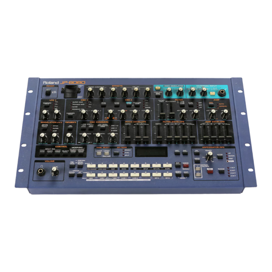
LOCATION OF CONTROLS ••••••••••••••••••••••••••••••••••••••••••••••••••••••••••••••••••••••••••••••••••••••••••••••••3
EXPLODED VIEW•••••••••••••••••••••••••••••••••••••••••••••••••••••••••••••••••••••••••••••••••••••••••••••••••••••••••••••4
PARTS LIST •••••••••••••••••••••••••••••••••••••••••••••••••••••••••••••••••••••••••••••••••••••••••••••••••••••••••••••••••5~6
IDENTIFYING THE VERSION NUMBER •••••••••••••••••••••••••••••••••••••••••••••••••••••••••••••••••••••••••••••••••7
SAVING AND LOADING USER DATA ••••••••••••••••••••••••••••••••••••••••••••••••••••••••••••••••••••••••••••••••••••7
FACTORY RESET•••••••••••••••••••••••••••••••••••••••••••••••••••••••••••••••••••••••••••••••••••••••••••••••••••••••••••••8
HOW TO UPDATE THE SOFTWARE •••••••••••••••••••••••••••••••••••••••••••••••••••••••••••••••••••••••••••••••••••••8
TEST MODE•••••••••••••••••••••••••••••••••••••••••••••••••••••••••••••••••••••••••••••••••••••••••••••••••••••••••••••••9~12
ERROR MESSAGE FOR MEMORY TEST •••••••••••••••••••••••••••••••••••••••••••••••••••••••••••••••••••••••••••••12
BLOCK DIAGRAM •••••••••••••••••••••••••••••••••••••••••••••••••••••••••••••••••••••••••••••••••••••••••••••••••••••••••••13
CIRCUIT BOARD •••••••••••••••••••••••••••••••••••••••••••••••••••••••••••••••••••••••••••••••••••••••••••••••••••••••14~16
CIRCUIT DIAGRAM ••••••••••••••••••••••••••••••••••••••••••••••••••••••••••••••••••••••••••••••••••••••••••••••••••••17~27
Copyright c 1998 by ROLAND CORPORATION
All rights reserved. No part of this publication may be reproduced in any form without the written permission of ROLAND CORPORATION.
17059936
JP-8080
SPECIFICATIONS
Synthesizer Section
Parts
2 (Upper, Lower)
Issued by RJA
Key Mode
Single, Dual, Split
Maximum Polyphony
10 Voices (Voice Modulator OFF)
8 Voices (Voice Modulator ON)
Page
Waveform
OSC 1
SUPER SAW
NOISE
SQUARE (PWM)
TRIANGLE
OSC 2
SQUARE (PWM)
TRIANGLE
Effects
Tone Control
Multi-FX (13 types)
SUPER CHORUS SLW, SUPER CHORUS MID, SUPER CHORUS FST, SUPER
CHORUS CLR, FLANGER SLOW, FLANGER DEEP, FLANGER FAST, DEEP
PHASING SLW, JET PHASING, TWISTING, FREEZE PHASE 1, FREEZE PHASE 2,
DISTORTION
Delay (5 types)
PANNING L->R, PANNING R->L, PANNING SHORT, MONO SHORT, MONO LONG
Internal Memory
Performances
Patches
Voice Modulator
Two 12-band band-pass filters
Noise
Robot Oscillator
Dedicated effect unit for Voice Modulator
(Ensemble, Delay)
Arpeggiator/RPS Section
Arpeggio Mode
UP
DOWN
UP&DOWN
RANDOM
Arpeggio Beat Patterns
1/4, 1/6, 1/8, 1/12, 1/16, 1/32, PORTA-A1--A11, PORTA-B1--B15, SEQUENCE-A1--
A7, SEQUENCE-B1--B5, SEQUENCE-C1--C2, SEQUENCE-D1--D8, ECHO1--3,
MUTE1--16, STRUMMING1--8, REFRAIN1--2, PERCUSSION1--4,
WALKING BASS, HARP, RANDOM (total 90 types)
Arpeggio Range
1 - 4 octave
Hold
ON/OFF
RPS Pattern Data (Internal Memory)
Patterns: 48
Maximum Loop Length (Measures): 4
Resolution
24 ticks per quarter note
Gate Time
REAL, STACCATO, 33%, 50%, 66%, 100%
Input Quantize
OFF, TRIPLET1/16, 1/16, TRIPLET1/8, 1/8, TRIPLET1/4, 1/4
Recording Method
Realtime (Loop Recording)
Tempo
20 to 250
Printed in Japan (ACE0) (CR)
1
TRIANGLE MOD
FEEDBACK OSC
SAW
SAW
NOISE
User
: 64
Preset
: 192
User
: 128
Preset
: 384
Advertisement

Related Manuals for Roland JP-8080


Summary of Contents for Roland JP-8080
-
Page 1: Specifications
Realtime (Loop Recording) Tempo 20 to 250 Copyright c 1998 by ROLAND CORPORATION All rights reserved. No part of this publication may be reproduced in any form without the written permission of ROLAND CORPORATION. 17059936 Printed in Japan (ACE0) (CR) - Page 2 JP-8080 Jul, 1998 Motion Control Section Motion Data (Internal Memory) Motions : 2 x 2 sets (SET A, B) Maximum Loop Length (Measures) Maximum Recording Length (Measures) : 99 Recording Method Realtime (Loop Recording and One Shot Recording) Tempo 20 to 250...
- Page 3 Jul, 1998 JP-8080 LOCATION OF CONTROLS [PARTS] PART No. PART NAME Qty. 32490595 P S-KEY MX BLK 01453245 PUSH SWITCH SDDLB1-B2-D-2 TV-5 01343101 D C-ESCT BX1H BLK 01458756 D C-ESCT HOLDER 01341178 CARD CONECTR CN015S-3013-0 00231401 U R-KNOB MF270 BLK/LCG 01560601 9M/M ROTARY POT.
-
Page 4: Exploded View
JP-8080 Jul, 1998 EXPLODED VIEW [PARTS] PART No. PART NAME 01458778 RACK ANGLE 01458712 BOTTOM COVER 12359139 FOOT FF-018 BLK 01458723 JACK HOLDER 01458701 TOP PANEL 01458734 PWR SPLY HOLDER 01561056 INSULATING SHEET 40016589 NYLON RIVET NRP-335 01458745 PWB HOLDER... - Page 5 Jul, 1998 JP-8080 00231878 TC74VHC00F QUAD NAND GATE IC30 on MB PARTS LIST 00567534 TC74VHC138F 3-TO-8 LINE DECODER IC16 on MB 00670290 TC74VHC139F DUAL 2-TO-4 LINE DECODER IC5 on MB 15289106 M5238AFP-600C OpAmp IC14 on MB 15189261 M5218AFP-600E OpAmp IC54,56 on MB...
- Page 6 JP-8080 Jul, 1998 01568245 RIBON CABLE 7X120-P2.0 PB CN3-MB CN6 01568512 RIBON CABLE 3X70-P2.0 PB CN4-MIB CN401 01568212 WIRING W3 VB CN601-MB CN10 01568534 RIBON CABLE 4X90-P2.0 PHB CN501-VB CN602 AC INLET 01347623 AC INLET NC-176-1.0 BATTERY 00238990 CR2032 220MAH/3V...
- Page 7 Jul, 1998 JP-8080 IDENTIFYING THE VERSION NUMBER (6)Press [WRITE]. (7)Press [DEC] or [INC] several times to select "ALL". (1)Turn the power on while holding down [LFO1 WAVEFORM], [NUMBER 1] and [NUMBER 3]. (2)The version number appears on the display. Type: [WRITE] (3)After checking the number, turn the power off.
-
Page 8: Factory Reset
Fig.5 appears. When loading one file ends, the display in Fig.6 appears. (1)The JP-8080 might not start up if mistakes are made in the version upgrade procedure or the power is cut during operation. -
Page 9: Test Mode
Jul, 1998 JP-8080 TEST MODE 2. MIDI Test (1) [fig.2] is shown on the LCD. Tools required [2] MIDI Test MIDI IN WAITING • MIDI cable • SmartMedia x2 (Formatted / Protected) [fig.2] • Oscillator (SINE WAVE of 1kHz, 800Hz) (2) Connect MIDI-IN and MIDI-OUT with a MIDI cable •... - Page 10 JP-8080 Jul, 1998 * If [fig6] does not appar on the LCD: Move all the sliders fully up and fully down. [fig.8] is shown on the LCD. The values displayed at the lower right of the LCD change within the ranges listed below as each volume or slider is moved.
- Page 11 VOCAL/UPPER INPUT LEVEL to the maximum. * If error: Connect the OUTPUT L and R of JP-8080 to the oscilloscope. · Check IC31, IC35, IC36(DAC), IC37, IC55 and IC56 on the Set the input range of the oscilloscope for 200mV/div.
- Page 12 JP-8080 Jul, 1998 (4) Is the sine wave which is proper level displayed on a screen of (2) Press [WRITE]. the oscilloscope? (3) [fig.18] is shown on the LCD. According to movement of the rotary volumes of INST/LOWER and VOCAL/UPPER, does the level of the sine wave on a screen...
- Page 13 Jul, 1998 JP-8080 BLOCK DIAGRAM Card Connector CN015S-3013-0 (CN202) LCD UNIT [16X2] for 5V SmartMedia [2M or 4M] RCM7044U-1A CARD BOARD ASSY SW BOARD ASSY [71017567] [71017578] AC IN 256Fs To IC32 XT1 IN Vocal Morph Sig. 64Fs To IC32 BCKIN IN...
- Page 14 JP-8080 Jul, 1998 PANEL BOARD ASSY (71017556)/CARD BOARD ASSY (71017567)/ MIC BOARD ASSY (71017589)/SW BOARD ASSY (71017578)/ PHONES BOARD ASSY (71017590) PANEL BOARD ASSY CARD BOARD ASSY (71017567) (71017556) MIC BOARD ASSY SW BOARD ASSY PHONES BOARD ASSY (71017589) (71017578)
- Page 15 Jul, 1998 JP-8080 PANEL BOARD ASSY (71017556)/CARD BOARD ASSY (71017567)/ MIC BOARD ASSY (71017589)/SW BOARD ASSY (71017578)/ PHONES BOARD ASSY (71017590) PANEL BOARD ASSY CARD BOARD ASSY (71017556) (71017567) PHONES BOARD ASSY SW BOARD ASSY MIC BOARD ASSY (71017590) (71017578)
- Page 16 JP-8080 Jul, 1998 MAIN BOARD ASSY (71017534) View from component side View from foil side...
- Page 17 Jul, 1998 JP-8080 CIRCUIT DIAGRAM CPU BLOCK C 8 7 A[0..18] L C D 1 0 0 . 1 L C D 9 I C 1 6 L C D 8 A 1 6 X L C D N I U...
- Page 18 JP-8080 Jul, 1998 ESP BLOCK I C 6 6 A E S P R E S X R E S T C 7 W 0 8 F R 5 2 R 3 1 R 3 3 R 4 3 R 4 5...
- Page 19 Jul, 1998 JP-8080 AD/DA BLOCK P C M 3 0 0 1 I C 3 2 C 2 4 2 1 0 / 1 6 I n p u t _ L C I N P L L R C I N...
- Page 20 JP-8080 Jul, 1998 INPUT BLOCK to PANEL C N 6 M I C _ I N A G N D I N - U - R T N I N - U - S E N D A G N D...
- Page 21 Jul, 1998 JP-8080 OUTPUT BLOCK D A 3 7 D A N 2 0 2 K +15V C 2 7 8 1 0 0 / 2 5 Q 1 0 R 1 6 5 R 1 6 6 2 S C 4 0 8 1...
- Page 22 JP-8080 Jul, 1998 MIDI BLOCK IN B IN A YKF51- 5041 N2012Z102T 01 C257 R109 N2012Z102T 01 IC45 R111 R115 N2012Z102T 01 PC410 DA35 DAN202K N2012Z102T 01 N2012Z102T 01 C262 R123 N2012Z102T 01 IC47 R125 120 R131 PC410 N2012Z102T 01...
- Page 23 Jul, 1998 JP-8080 CARD BLOCK D[8..15] C237 IC41A IC40 T C74HC32AF RA27 XHWR XCWR XCARD XCARD XCRE BDIR T C 74HCT245AF IC41B T C74HC32AF C WPSNS IC38B 100k XEJECT XRES C239 T C7W08F C238 IC42 BDIR R100 XCCE IC41C XCRE...
- Page 24 JP-8080 Jul, 1998 CN BLOCK SD[0..7] 100p*9 IL-FPC-14ST- N CN11 SC[0..7] TO LCD UNIT 10/16 + 15 100p*8 - 15 LSC-EN1 100P LSC-EN0 TO PANEL BOARD LSC2 LSC1 100P LSC0 ADC2 ADC1 ADC0 AN[2..7] (100*4)*3 VR48-41 VR40-33 VR32-25 VR24-17 VR16-9...
- Page 25 Jul, 1998 JP-8080 PANEL & OTHERS V R 1 A V R 2 A E V U JFU FL1 B24 E V U JFU FL1 B24 1 0 0 V R 8 - 1 IC1A UPC4570HA 1 0 0 1 0 0 0.01...
- Page 26 JP-8080 Jul, 1998 V R 2 7 A V R 2 8 A R 5 6 D 8 6 D 8 7 D 8 5 UPPER R S 3 0 1 1 1 A 9 R S 3 0 1 1 1 A 9...
- Page 27 Jul, 1998 JP-8080 CN602 CN202 PHONES-L CN201 P H ONES-R FGND to PHONES FGND SENS2 SENS1 to MAIN for Smart-Media 5 1048-0400 + 15 + 15 C603 IC601B CN601 I/O8 10/50 I/O7 IC601C IC601A FGND I/O6 UPC4570C I/O5 C604 UPC4570C...