Table of Contents
Advertisement
Quick Links
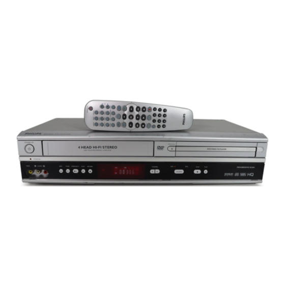
DVD + VCR Combi
Service
Service
Service
Service Manual
Contents
Schematic Diagrams and CBA's
Mechanical and Electrical Parts Lists
This service manual is for DVP3050V/55 Second
Generation model, which is different from the
previous generation DVP3050V/55 models.
For Second Generation model, the serial number
begins with xx2Bxxxxxxxxxx.
For technical data reference is made to the Service
Manual of the previous generation DVP3050V/55
12NC: 3139 785 31000. This manual shows only the
differences.
c Copyright 2005 Philips Consumer Electronics B.V. Eindhoven, The Netherlands.
All rights reserved. No part of this publication may be reproduced, stored in a retrieval
system or transmitted, in any form or by any means, electronic, mechanical, photocopying,
or otherwise without the prior permission of Philips.
Published by FU-KC 0517 Service AV Systems
Survey of versions:
/55
NTSC
Printed in The Netherlands
SUPPLEMENT
DVP3050V/
Second Generation
CLASS 1 LASER PRODUCT
KLASSE 1 LASER PRODUKT
KLASS 1 LASER APPARAT
CLASSE 1 PRODUIT LASER
Rating label
xx2Bxxxxxxxxxx
Serial number
Subject to modification
55
U JAN 2005
H982BMD
EN 3139 785 31300
Advertisement
Table of Contents

Related Manuals for Philips DVP3050V/55


Summary of Contents for Philips DVP3050V/55
- Page 1 12NC: 3139 785 31000. This manual shows only the differences. c Copyright 2005 Philips Consumer Electronics B.V. Eindhoven, The Netherlands. All rights reserved. No part of this publication may be reproduced, stored in a retrieval system or transmitted, in any form or by any means, electronic, mechanical, photocopying, or otherwise without the prior permission of Philips.
- Page 2 Different parts from the previous generation DVP3050V/55 model ....... .
-
Page 3: Block Diagrams
[ DVP3050V/55 (Second Generation) ] BLOCK DIAGRAMS <VCR SECTION> Servo / System Control Block Diagram H982BBLS 1-12-1... -
Page 4: Video Block Diagram
Video Block Diagram H982BBLV 1-12-2... -
Page 5: Audio Block Diagram
Audio Block Diagram H982BBLA 1-12-3... -
Page 6: Hi-Fi Audio Block Diagram
Hi-Fi Audio Block Diagram H982BBLH 1-12-4... -
Page 7: Power Supply Block Diagram
Power Supply Block Diagram H982BBLP 1-12-5... - Page 8 BLOCK DIAGRAMS <DVD SECTION> DVD System Control / Servo Block Diagram 1-12-6 H982BBLSD...
-
Page 9: Digital Signal Process Block Diagram
Digital Signal Process Block Diagram 1-12-7 H982BBLD... -
Page 10: Dvd Video / Audio Block Diagram
DVD Video / Audio Block Diagram 1-12-8 H982BBLVD... - Page 11 [ DVP3050V/55 (Second Generation) ] Main 1/8 Schematic Diagram Parts Location Guide < VCR Section > Ref No. Position Ref No. Position CAPACITORS RESISTORS C023 JC08 C502 R502 C505 R503 C507 R504 C508 R507 C509 R508 C511 R511 C512 R517...
- Page 12 Main 1/8 Schematic Diagram < VCR Section > IC501 KEY VOLTAGE CHART Pin No. KEY 1 (67 PIN) KEY 2 (66 PIN) “ “ = SMD Voltage indications for PLAY, REC and DVD modes Voltage 0.00 ~ 0.51V POWER DVD/VCR on the Schematic Diagrams are as shown below: 0.51 ~ 0.92V CH UP...
- Page 13 Main 2/8, Power SW & Sensor Schematic Diagram < VCR Section > FIP502 MATRIX CHART SACD “ “ = SMD Voltage indications for PLAY, REC and DVD modes REPEAT PSCAN on the Schematic Diagrams are as shown below: PLAY mode REC mode (2.5) DVD mode...
- Page 14 Main 2/8 Schematic Diagram Parts Location Guide < VCR Section > Ref No. Position Ref No. Position CAPACITORS RESISTORS C540 R571 C550 R572 C571 R573 C572 R574 C574 R575 C701 R576 C703 R580 C704 R585 C708 R586 C709 R587 CONNECTOR R588 CN509 R590...
- Page 15 Main 3/8 Schematic Diagram Parts Location Guide < VCR Section > Ref No. Position Ref No. Position Ref No. Position CAPACITORS CAPACITORS RESISTORS C301 C406 R310 C302 C407 R311 C303 C408 R314 C304 C409 R315 C305 C410 R316 C307 C411 R317 C308 C412...
- Page 16 Main 3/8 Schematic Diagram < VCR Section > Voltage indications for PLAY, REC and DVD modes “ “ = SMD on the Schematic Diagrams are as shown below: PLAY mode REC mode (2.5) DVD mode < > The same voltage for Indicates that the voltage PLAY, REC &...
- Page 17 Main 4/8 Schematic Diagram < VCR Section > “ “ = SMD Voltage indications for PLAY, REC and DVD modes on the Schematic Diagrams are as shown below: PLAY mode REC mode (2.5) DVD mode < > The same voltage for Indicates that the voltage PLAY, REC &...
- Page 18 Main 4/8 Schematic Diagram Parts Location Guide < VCR Section > Ref No. Position Ref No. Position Ref No. Position CAPACITORS CAPACITORS RESISTORS C1201 C1532 R1224 C1202 C1535 R1225 C1205 C1536 R1226 C1206 C1537 R1238 CONNECTOR C1207 R1240 C1208 CN1601 R1245 DIODE C1221...
- Page 19 Main 5/8 Schematic Diagram Parts Location Guide < VCR Section > Ref No. Position Ref No. Position CAPACITORS RESISTORS C370 R391 AA-3 C371 R392 AA-3 C391 AA-3 R395 AA-3 C392 AA-3 R397 AA-3 C751 AA-2 R751 AA-2 C752 AA-2 R752 AA-1 C753 R753...
- Page 20 Main 5/8 Schematic Diagram < VCR Section > “ “ = SMD Voltage indications for PLAY, REC and DVD modes on the Schematic Diagrams are as shown below: PLAY mode REC mode (2.5) DVD mode < > The same voltage for Indicates that the voltage PLAY, REC &...
- Page 21 Main 6/8 & DVD Open/Close Schematic Diagram < VCR Section > “ “ = SMD Voltage indications for PLAY, REC and DVD modes on the Schematic Diagrams are as shown below: PLAY mode REC mode (2.5) DVD mode < > The same voltage for Indicates that the voltage PLAY, REC &...
- Page 22 Main 6/8 Schematic Diagram Parts Location Guide < VCR Section > Ref No. Position Ref No. Position CAPACITORS TRANSISTORS C051 AG-3 Q1008 AJ-2 C053 AF-3 Q1011 AD-2 RESISTORS C1030 AD-3 C1031 AD-3 R056 AG-4 C1039 AD-3 R057 AG-3 C1040 AC-3 R058 AF-3 C1042...
- Page 23 Main 7/8 Schematic Diagram Parts Location Guide < VCR Section > Ref No. Position Ref No. Position CAPACITORS DIODES C013 AL-4 D1024 AJ-1 C018 AL-3 D1025 AJ-1 C020 AL-3 D1026 AJ-2 C021 AL-3 C030 AL-1 IC1001 AK-1 COILS C1001 AI-3 C1002 AL-3 L009...
- Page 24 Main 7/8 Schematic Diagram < VCR Section > CAUTION ! CAUTION ! Voltage indications for PLAY, REC and DVD modes on the Schematic Diagrams are as shown below: For continued protection against fire hazard, Fixed voltage (or Auto voltage selectable) power supply circuit is used in this unit. replace only with the same type fuse.
- Page 25 Main 8/8 Schematic Diagram < VCR Section > Voltage indications for PLAY, REC and DVD modes “ “ = SMD on the Schematic Diagrams are as shown below: PLAY mode REC mode (2.5) DVD mode < > The same voltage for Indicates that the voltage PLAY, REC &...
-
Page 26: Top View
Main CBA Top View CAUTION ! Because a hot chassis ground is present in the power CAUTION ! DVD Open/Close supply circut, an isolation transformer must be used. For continued protection against fire hazard, Fixed voltage (or Auto voltage selectable) power supply circuit is used in this unit. CBA Top View replace only with the same type fuse. -
Page 27: Main Cba Bottom View
Main CBA Bottom View CAUTION ! CAUTION ! Because a hot chassis ground is present in the power Fixed voltage (or Auto voltage selectable) power supply circuit is used in this unit. For continued protection against fire hazard, supply circut, an isolation transformer must be used. If Main Fuse (F1001) is blown , check to see that all components in the power supply replace only with the same type fuse. -
Page 28: Main Cba Parts Location Guide
Main CBA Parts Location Guide Ref No. Position Ref No. Position Ref No. Position Ref No. Position Ref No. Position Ref No. Position Ref No. Position Ref No. Position Ref No. Position Ref No. Position Ref No. Position CAPACITORS CAPACITORS CAPACITORS CAPACITORS DIODES... -
Page 29: Lead Identifications
LEAD IDENTIFICATIONS [ DVP3050V/55 (Second Generation) ] 2SK3543 2SA1175(J,H,F) 2SA1015-GR(TPE2) 2SK3757(Q) 2SC2785(J,H,F,K) 2SA1015-GR(TE2 F T) BA1F4M-T 2SC1815-(BL,Y)(TPE2) BN1F4M-T 2SC1815-(BL,GR,Y)(TE2 F T) KRA103M 2SC2120-Y(TE2 F T) KRC103M 2SC2120-Y(TPE2) KTA1266(GR) KTC3198(Y,GR) KTA1267(GR,Y) KTC3203(Y) KTA1267-GR-AT/P KTC3203-Y-AT/P KTA1267Y-AT/P KTC3193(Y) KTC3199(Y,GR,BL) G D S KTC3199(Y,GR,BL)-AT/P... -
Page 30: Electrical Parts List
1-19-1 ELECTRICAL PARTS LIST MISCELLANEOUS SW515 * 4822 276 14127 SKQSAF001A 9965 000 29222 MCV CBA (This assembly can be used to replace the first Generation board - 9965 SW515 * 9965 000 19590 TACT SWITCH TC-1104(H=9.5) SW516 4822 276 13954 KSM0614B 000 27560) SW516 * 4822 276 14127... - Page 31 1-19-2 ELECTRICAL PARTS LIST RESISTORS R1043 * 9965 000 19607 $ MET OXIDE RES. 1W J 2.7 OHM D082 * 9965 000 23978 1N4005 D100 4822 130 30621 1N4148 COILS & FILTERS D100 * 4822 130 32778 1SS133 L009 9965 000 05702 CHOKE COIL 47UH-K D101 4822 130 30621...
- Page 32 1-19-3 ELECTRICAL PARTS LIST DIODES D1038 * 9965 000 23978 1N4005 Q567 * 4822 130 11647 2SC2785J D1058 4822 130 31933 1N5061 Q567 * 9965 000 19583 TRANSISTOR 2SC2785(H) D1058 * 9965 000 23978 1N4005 Q567 * 9965 000 05643 TRANSISTOR 2SC2785(F) D1301 9965 000 08622...
- Page 33 1-19-4 INTEGRATED CIRCUITS IC501 9965 000 28853 SYSCON IC MN101D08DES IC571 9965 000 19575 FL DRIVER IC PT6313-S-TP IC571 * 9965 000 23985 VFD DRIVER IC SC16313 IC571 * 9965 000 27576 VFD DR/CONT IC PT6313-S-TP(L) IC571 * 9965 000 27577 VFD DRIVER IC SC16313G IC751 9965 000 23979...