Sony NW-S603 Service Manual
Digital music player
Hide thumbs
Also See for NW-S603:
- Operation manual (113 pages) ,
- Quick start manual (14 pages) ,
- Operation manual (113 pages)
Table of Contents
Advertisement
Quick Links
SERVICE MANUAL
Ver. 1.2 2006.12
• SonicStage and the SonicStage logo are trademarks or registered trademarks of Sony Corporation.
• OpenMG, ATRAC, ATRAC3, ATRAC3plus, ATRAC Advanced Lossless and their logos are trademarks of Sony Corporation.
• "WALKMAN" and "WALKMAN" logo are registered trademarks of Sony Corporation.
• Microsoft, Windows, Windows NT and Windows Media are trademarks or registered trademarks of Microsoft Corporation in the United States and/or other countries.
• Adobe and Adobe Reader are trademarks or registered trademarks of Adobe Systems Incorporated in the United States and/or other countries.
• MPEG Layer-3 audio coding technology and patents licensed from Fraunhofer IIS and Thomason.
• IBM and PC/AT are registered trademarks of International Business Machines Corporation.
• Macintosh is a trademark of Apple Computer, Inc.
• Pentium is a trademark or a registered trademark of Intel Corporation.
• CD and music-related data from Gracenote, Inc., copyright © 2000-2006 Gracenote. Gracenote Software, copyright © 2000-2006 Gracenote. This product and service
may practice one or more of the following U.S. Patents: #5,987,525; #6,061,680; #6,154,773, #6,161,132, #6,230,192, #6,230,207, #6,240,459, #6,330,593, and other patents
issued or pending. Some services supplied under license from Open Globe, Inc. for U.S. Patent: #6,304,523. Gracenote and CDDB are registed trademarks of Gracenote.
The Gracenote logo and logotype, and the "Powered by Gracenote" logo are trademarks of Gracenote.
• All other trademarks and registered trademarks are trademarks or registered trademarks of their respective holders. In this manual,
Audio compression technology
– MPEG-1 Audio Layer-3 (MP3)
– Windows Media Audio (WMA)*
– Adaptive Transform Acoustic Coding (ATRAC)
– Advanced Audio Coding (AAC)*
– Linear-PCM (PCM)
* Copyright protected WMA/AAC files cannot be played back.
Maximum recordable number of songs and time (Approx.)
The approximate times are based on a transferred or recorded 4-minute ATRAC*, MP3 or Linear-PCM
format song. Other playable audio file formats may be different from ATRAC or MP3 format.
* Except ATRAC Advanced Lossless. Compression rate of ATRAC Advanced Lossless varies depending on songs.
For example, one CD (containing 15 4-minute songs) is approximately 200 to 500 MB.
NW-S603/S703F
Bit rate
Songs
Time
48 kbps
685
45 hr. 40 min.
64 kbps
510
34 hr. 00 min.
66 kbps
500
33 hr. 20 min.
96 kbps
340
22 hr. 40 min.
128 kbps
255
17 hr. 00 min.
132 kbps
250
16 hr. 40 min.
160 kbps
205
13 hr. 40 min.
192 kbps
170
11 hr. 20 min.
256 kbps
125
8 hr. 20 min.
320 kbps
100
6 hr. 40 min.
352 kbps
94
6 hr. 10 min.
1411 kbps
23
1 hr. 30 min.
(Linear-PCM)
NW-S706F
Bit rate
Songs
Time
48 kbps
2700
180 hr. 00 min.
64 kbps
2000
133 hr. 20 min.
66 kbps
2000
133 hr. 20 min.
96 kbps
1350
90 hr. 00 min.
128 kbps
1000
66 hr. 40 min.
132 kbps
1000
66 hr. 40 min.
Sony Corporation
9-887-449-03
Connect Business Division
2006L05-1
Published by Sony Techno Create Corporation
© 2006.12
NW-S603/S605/S703F/
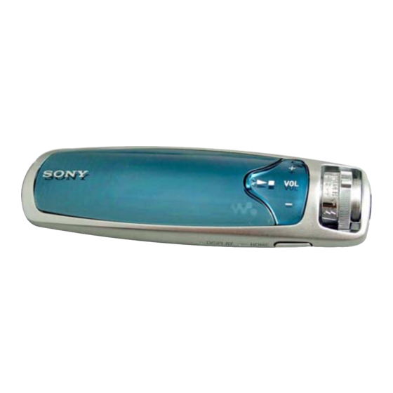
Photo: NW-S603
SPECIFICATIONS
NW-S605/S705F
Songs
Time
1350
90 hr. 00 min.
1000
66 hr. 40 min.
995
66 hr. 20 min.
680
45 hr. 20 min.
515
34 hr. 20 min.
495
33 hr. 00 min.
410
27 hr. 20 min.
340
22 hr. 40 min.
255
17 hr. 00 min.
205
13 hr. 40 min.
185
12 hr. 20 min.
47
3 hr. 00 min.
S705F/S706F
Canadian Model
NW-S603/S605/S703F/S705F/S706F
NW-S603/S703F/S705F/S706F
Australian Model
TM
®
and
marks are not specified.
Bit rate
Songs
Time
160 kbps
820
54 hr. 40 min.
192 kbps
685
45 hr. 40 min.
256 kbps
515
34 hr. 20 min.
320 kbps
410
27 hr. 20 min.
352 kbps
375
25 hr. 00 min.
1411 kbps
94
6 hr. 10 min.
(Linear-PCM)
Capacity (User available capacity)*
NW-S603/S703F: 1 GB (Approx. 968 MB = 1,015,726,080 bytes)
NW-S605/S705F: 2 GB (Approx. 1.89 GB = 2,035,974,144 bytes)
NW-S706F: 4 GB (3.79 GB = 4,075,716,608 bytes)
* Available storage capacity of the player may vary.
A portion of the memory is used for data management functions.
Supported bit rates
MP3: 32 to 320 kbps variable bit rate-compliant
WMA: 32 to 192 kbps variable bit rate-compliant
ATRAC: 48/64/66 (ATRAC3)*/96/105 (ATRAC3)*/128/132 (ATRAC3)/160/192/256/320/352 kbps
*
CD recording cannot be done using the SonicStage software in ATRAC3 at 66/105 kbps.
ATRAC Advanced Lossless*: 64/128/132 (ATRAC3 base layer)/ 256/352 kbps
*
The bit rate description of ATRAC Advanced Lossless shows the bit rate for the contents which enables fast transfer
to ATRAC compatible devices or media.
AAC: 16 to 320 kbps variable bit rate-compliant*
* Nonstandard bit rates or non-guaranteed bit rates are included depending on the sampling frequency.
Linear-PCM: 1411 kbps
Sampling frequency*
MP3: 32, 44.1, 48 kHz
WMA: 44.1 kHz
ATRAC: 44.1 kHz
AAC: 11.025, 12, 16, 22.05, 24, 32, 44.1, 48 kHz
Linear-PCM: 44.1 kHz
* Sampling frequency may not correspond to all encoders.
DIGITAL MUSIC PLAYER
US Model
NW-S703F/S705F
NW-S603/S705F/S706F
AEP Model
UK Model
E Model
Tourist Model
NW-S703F/S705F/S706F
Chinese Model
NW-S603/S605/S705F
– Continued on next page –
Advertisement
Table of Contents

Related Manuals for Sony NW-S603


Summary of Contents for Sony NW-S603
-
Page 1: Specifications
• SonicStage and the SonicStage logo are trademarks or registered trademarks of Sony Corporation. • OpenMG, ATRAC, ATRAC3, ATRAC3plus, ATRAC Advanced Lossless and their logos are trademarks of Sony Corporation. • “WALKMAN” and “WALKMAN” logo are registered trademarks of Sony Corporation. -
Page 2: Table Of Contents
87.2 × 27.4 × 14.9 mm (3.4 × 0.9 × 0.6 inches) (w/h/d, projecting parts not included) EXPLODED VIEWS Mass Approx. 47 g (Approx. 2 oz) 6-1. Cover (Rear) Assy Section (NW-S603/S605) ....38 6-2. Cover (Rear) Assy Section Supplide Accessories Please check the accessories in the package. (NW-S703F/S705F/S706F) ..........39 Headphones (1) 6-3. -
Page 3: Servicing Notes
NW-S603/S605/S703F/S705F/S706F SECTION 1 SERVICING NOTES NOTE THE MAIN BOARD REPLACING UNLEADED SOLDER When the MAIN board is replaced, format it according to the Boards requiring use of unleaded solder are printed with the lead- following. free mark (LF) indicating the solder contains no lead. - Page 4 NW-S603/S605/S703F/S705F/S706F Ver. 1.2 COLOR VARIATION COLOR Model Destination BLACK BLUE GOLD PINK VIOLET CND (Clamshell) NW-S603 NW-S605 US (Clamshell) NW-S703F E, AUS, JE US (Clamshell) CND (Clamshell) NW-S705F E, AUS, JE CND (Clamshell) NW-S706F E, AUS, JE • Abbreviation AUS : Australian model...
-
Page 5: General
Noise Canceling does not work with the DISPLAY/HOME button. models without the Noise Canceling Switch the display to the Power Save function (NW-S603/S605), even if mode when you do not operate the the supplied headphones are used. player for a while. -
Page 6: Disassembly Flow
NW-S603/S605/S703F/S705F/S706F SECTION 3 DISASSEMBLY • This set can be disassembled in the order shown below. 3-1. DISASSEMBLY FLOW Note 1: The process described in can be performed in any order. Note 2: Without completing the process described in , the next process can not be performed. -
Page 7: Cover (Rear) Assy
NW-S603/S605/S703F/S705F/S706F Note: Follow the disassembly procedure in the numerical order given. 3-2. COVER (REAR) ASSY knob (hold) switch (S505) 4 Remove the cover (rear) assy in the direction of arrow A . 3 screw (B1.4) 1 two claws 2 knob (hold) Note1: Knob (hold) cannot re-used. -
Page 8: Button (3D) Assy
NW-S603/S605/S703F/S705F/S706F Ver. 1.1 3-4. BUTTON (3D) ASSY 1 Open the button (3D) assy. 3 button (3D) assy 2 Remove the convex portion. 3-5. HOLDER (REAR) 4 two self tap screws 2 adhesive sheet (sound) 1 button (sound) 6 holder (rear) -
Page 9: Main Board Scetion
NW-S603/S605/S703F/S705F/S706F Ver. 1.1 3-6. MAIN BOARD SECTION 1 Set the knob (JOG) to the position of FOLDER. knob (JOG) 7 OLED sub assy flexible board (CN401) 2 sheet (wire) knob (JOG) 9 connector (CN801) 8 Peel copper leaf (tuner) from the MAIN board. -
Page 10: Oled Sub Assy
NW-S603/S605/S703F/S705F/S706F Ver. 1.1 3-8. OLED SUB ASSY 1 film sheet (OEL) 4 two screws (B1.4) 6 OLED sub assy 3 adhesive sheet (SW PWB) Note: Adhesive Sheet (SW PWB) cannot re-used. Please replace to brand-new part ones adhesive sheet (SW PWB) is removed. -
Page 11: Knob (Jog)
NW-S603/S605/S703F/S705F/S706F 3-10. KNOB (JOG) knob (JOG) 1 Push the knob (JOG) in the derection of the arrow. 2 two claws 3 JOG block 4 knob (JOG) -
Page 12: Headphone Assy
NW-S603/S605/S703F/S705F/S706F 3-11. HEADPHONE ASSY 1 two claws 2 cover (JOG) NOTE WHEN ASSEMBLING THE HOLDER (JOG) Assemble the holder (JOG), meeting its concave portion with the spring (JOG) as shown in the figure. holder (JOG) concave portion 5 holder (JOG) -
Page 13: Test Mode
NW-S603/S605/S703F/S705F/S706F SECTION 4 TEST MODE HOW TO ENTER THE TEST MODE 5. CHARGE CURRENT SELECT 1. While keeping pressing the and operate the set in order 1. While the set is in the TEST MODE (HOLD:ON), turn the below (Both of the position of Jog shuttle are acceptable). -
Page 14: Block Diagram
NW-S603/S605/S703F/S705F/S706F SECTION 5 DIAGRAMS 5-1. BLOCK DIAGRAM CN106 (1/2) (WM-PORT) HP_L HP_L HPOUTL 33 HP_R D– HPOUTR 36 • SIGNAL PATH HP_R : AUDIO MIC SWITCH MIC_L AU_L_IN 13 MLININL BEEP/GPIOL4 57 FILTER IC3001 MIC_L AU_R_IN 16 MLININR BEEPEN 65... - Page 15 NW-S603/S605/S703F/S705F/S706F • Note for Printed Wiring Boards and Schematic Diagrams Note on Printed Wiring Board: Note on Schematic Diagram: • X : parts extracted from the component side. • All capacitors are in µF unless otherwise noted. (p: pF) • Y : parts extracted from the conductor side.
-
Page 16: Printed Wiring Board - Main Board (Side A)
NW-S603/S605/S703F/S705F/S706F 5-2. PRINTED WIRING BOARD – MAIN Board (Side A) – : Uses unleaded solder. MAIN BOARD (SIDE A) OLED SUB ASSY R408 (NW-S703F/S705F/S706F) R3034 C3026 C3013 R3023 C418 R3019 C419 C420 (NW-S703F/S705F/S706F) S507 PLAY MODE, R125 SOUND C3027 JL102... -
Page 17: Printed Wiring Board - Main Board (Side B)
NW-S603/S605/S703F/S705F/S706F 5-3. PRINTED WIRING BOARD – MAIN Board (Side B) – : Uses unleaded solder. MAIN BOARD (SIDE B) LITHIUM ION BATTERY 3.7V 320mA (NW-S703F/S705F/S706F) R3039 C3002 JL501 Q3001 ∗ R3043 IC3007 B2B1 C3029 A2A1 R3038 R106 R3041 FB113 R107... -
Page 18: Schematic Diagram - Main Board (1/7)
NW-S603/S605/S703F/S705F/S706F • See page 33 for IC Pin Function Description. 5-4. SCHEMATIC DIAGRAM – MAIN Board (1/7) – (1/7) MAIN BOARD VDD_UNREG VDD_AD2.0 (Page VDD_CORE1.2 MAIN VDD_IO2.8 BOARD DGND (7/7) VDD_USB3.3 VDR107 VDD_NAND2.8 R-IN L-IN (NW-S603/S605) C2118 C2117 R2107 0.022... -
Page 19: Schematic Diagram - Main Board (2/7)
NW-S603/S605/S703F/S705F/S706F 5-5. SCHEMATIC DIAGRAM – MAIN Board (2/7) – MAIN BOARD (2/7) TU_OUTL (Page CN108 TU_OUTL R-IN TU_OUTR L-IN TU_OUTR MAIN BOARD VDD_NAND2.8 NAND_RB1 NAND_RB1 (5/7) MAIN_XRST MAIN_XRST NAND_RB0 NAND_RB0 BIU_XCS0 NAND_XCE1 BIU_XCS0 NAND_XCE1 BIU_XCS1 BIU_XCS1 NAND_XWP NAND_XWP BIU_XRE BIU_XRE... -
Page 20: Schematic Diagram - Main Board (3/7)
NW-S603/S605/S703F/S705F/S706F • See page 29 for IC Block Diagrams. 5-6. SCHEMATIC DIAGRAM – MAIN Board (3/7) – (3/7) MAIN BOARD DGND BIU_D15 BIU_D15 VDD_IO2.8 MAIN R201 BIU_D14 R202 BOARD BIU_D14 100k (7/7) BIU_D13 (Page 24) BIU_D13 BIU_D12 BIU_D12 BIU_D11 BIU_D11... -
Page 21: Schematic Diagram - Main Board (4/7)
NW-S603/S605/S703F/S705F/S706F • See page 29 for IC Block Diagrams. 5-7. SCHEMATIC DIAGRAM – MAIN Board (4/7) – MAIN BOARD (4/7) TU_DA TU_SCK MAIN BOARD VDD_TU2.7 (5/7) (Page 22) R3024 NC_LOUT R3041 R3002 R3016 R3033 100k 2700 Q3002 R3022 C3027 0.033... -
Page 22: Schematic Diagram - Main Board (5/7)
NW-S603/S605/S703F/S705F/S706F • See page 29 for IC Block Diagrams. 5-8. SCHEMATIC DIAGRAM – MAIN Board (5/7) – MAIN BOARD (5/7) TU_SCK TU_SCK TU_LA MAIN TU_DA TU_DA BOARD TU_STO VDD_TU2.7 (4/7) (Page 21) TU_CLKON MAIN R2706 R2701 BOARD R2702 C2708 4700... -
Page 23: Schematic Diagram - Main Board (6/7)
NW-S603/S605/S703F/S705F/S706F • See page 29 for IC Block Diagrams. 5-9. SCHEMATIC DIAGRAM – MAIN Board (6/7) – CN401 (6/7) MAIN BOARD VDD1(17V) VDD3(12V) C416 L401 D401 22uH MA21D3800LS0 C421 VGH(9V) C417 VCC(12V) OEL_DC OEL_DC VCC(12V) OEL_XRST OEL_XRST OEL_XCS OEL_XCS OEL_DISP_ON... -
Page 24: Schematic Diagram - Main Board (7/7)
NW-S603/S605/S703F/S705F/S706F Ver. 1.1 • See page 29 for IC Block Diagrams. 5-10. SCHEMATIC DIAGRAM – MAIN Board (7/7) – MAIN BOARD (7/7) MAIN VDD_IO2.8 BOARD (1/7) DGND (Page 18) R611 MAIN VDD_IO2.8 R617 470k JL619 BOARD (3/7) DGND (Page 20) VDD_UNREG VDD_IO2.8... -
Page 25: Printed Wiring Board - Sub Board
NW-S603/S605/S703F/S705F/S706F 5-12. SCHEMATIC DIAGRAM – SUB Board – 5-11. PRINTED WIRING BOARD – SUB Board – : Uses unleaded solder. SUB BOARD SUB BOARD (SIDE A) IC1301 (NW-S706F) R1306 NAND FLASH ROM IC1301 TC58NVG3D4CTGOO(NW-S603/S703F) TH58NVG4D4CTGOO(NW-S605/S705F) K9HBG08U1M-PCB(NW-S706F) R1303 IC1301 CN1301 (NW-S706F) -
Page 26: Printed Wiring Board - Switch Board (Side A)
NW-S603/S605/S703F/S705F/S706F 5-13. PRINTED WIRING BOARD – SWITCH Board (Side A) – : Uses unleaded solder. SWITCH BOARD (SIDE A) S552 VOL – R555 VDR553 R552 R557 JL802 R580 FB855 X801 S551 VDR852 VDR851 JL801 FB854 S554 VOL + (11) 1-871-592-... -
Page 27: Printed Wiring Board - Switch Board (Side B)
NW-S603/S605/S703F/S705F/S706F 5-14. PRINTED WIRING BOARD – SWITCH Board (Side B) – : Uses unleaded solder. SWITCH BOARD (SIDE B) C851 C852 R852 FB852 FB853 R853 S555 FOLDER – (Page 17) MAIN BOARD CN107 C801 R801 HEADPHONE CN852 CN801 ASSY R803... -
Page 28: Schematic Diagram - Switch Board
NW-S603/S605/S703F/S705F/S706F • See page 29 for IC Block Diagrams. 5-15. SCHEMATIC DIAGRAM – SWITCH Board – SWITCH BOARD R563 R554 R553 R555 R557 R559 R560 Q553 2SC584600LS0 Q552 C551 VDR551 2SA207800LS0 0.01 CN801 R562 S554 S556 S555 R561 S552 100k VDD_RTC2.8... -
Page 29: Ic Block Diagrams
NW-S603/S605/S703F/S705F/S706F • IC Block Diagrams – MAIN Board – IC201 S71PL032J08BFW0B0 47 46 45 44 43 42 NC 41 DQ15 SECTOR 40 DQ13 SWITCHES 39 DQ4 38 DQ3 ERASE VOLTAGE 37 DQ9 INPUT/OUTPUT GENERATOR BUFFERS XWP/ACC 36 XOE STATE 35 XCE1F... - Page 30 NW-S603/S605/S703F/S705F/S706F IC601 MAX8670A 32 31 THERMAL-OVERLOAD REG5 PROTECTION ABOVE TJ=+165 C USB_SUS 3.3V USB LDO 3.3V USB_H/L REGURATOR USB_IN1 1MHz OSC USB_IN2 USB POWER MANAGEMENT SYS1 30 EN SYS2 29 PG_AORE 28 LX_CORE CORE STEP-DOWN LI+BATTERY INPUT LIMITER REGULATOR 27 IN_CORE...
- Page 31 NW-S603/S605/S703F/S705F/S706F IC2702 SDFMM1N23GB2T 14 13 12 11 X2 10 X1 9 CL 8 LA BUFFER LOGIC MPX DECODER LAG-LEAD FILTER TUNING SYSTEM DEMODULATOR ANTENNA LIMITER BALUN FILTER RSSO RSSI 5 6 7 IC3004 MAX5489ETE IC3001 NLAS4717EPFCT1G 14 13 8-BIT DECODER...
- Page 32 NW-S603/S605/S703F/S705F/S706F – SWITCH Board – X801 RX-4574LC 32.768KHz CONTROL LINE N.C. DIVIDER N.C. CLOCK AND CALENDAR /TIRQ /AIRQ FCON TIMER OUTPUT REGISTER FOUT CONTROLLER ALARM REGISTER INTERRUPTS CONTROLLER CONTROL REGISTER INTERFACE SHIFT CIRCUIT REGISTER 12 VDD 11 CE1 10 CLK...
- Page 33 NW-S603/S605/S703F/S705F/S706F • IC Pin Function Description MAIN BOARD IC101 CXD5090B1-003GG (CPU) Pin No. Pin Name Description NAD0/GPIOC0 to 1 to 8 Data signal input from the NAND flash ROM NAD7/GPIOC7 NCLE/GPIOC8 Command latch enable signal output to the NAND flash ROM...
- Page 34 NW-S603/S605/S703F/S705F/S706F Pin No. Pin Name Description T1/GPIOL1 LINE amplifier power supply ON/OFF control signal output terminal EC2/INT7/ Headphone detection signal input terminal GPIOL2 T3/GPIOL3 Power supply ON/OFF control signal output terminal for the NAND flash ROM BEEP/GPIOL4 Beep signal output terminal...
- Page 35 NW-S603/S605/S703F/S705F/S706F Pin No. Pin Name Description MSSCLK Not used MSDIO0/ Not used GPIOE1 MSDIO1/ GPIOE2 to 101 to 103 Battery charge control signal output to the power control IC MSDIO3/ GPIOE4 MSINS/GPIOE5 Not used MCSEL Not used CBIAS Not used...
- Page 36 NW-S603/S605/S703F/S705F/S706F Pin No. Pin Name Description FS256 Not used LRCK/WS Not used BCK/SCK Not used ADDT/SDI/ Not used GPIOM0 DADT/SDO/ Not used GPIOM1 MUTFGL/ Chip enable signal output to the gain control GPIOM2 MUTFGR/ Model setting terminal GPIOM3 Ground terminal...
- Page 37 NW-S603/S605/S703F/S705F/S706F Pin No. Pin Name Description DVDK2 Power supply terminal Ground terminal RTCVDD Power supply terminal RTCREGO Power supply voltage output (+2.8V) to the real time clock RTCVREF Reference voltage terminal Not used RTCGND Ground terminal D8/GPIOA12 to 222 to 229...
-
Page 38: Exploded Views
: Tourist model : Korean model Parts Color Cabinet's Color electrical parts list. MX : Mexican model 6-1. COVER (REAR) ASSY SECTION (NW-S603/S605) Note: The illustration sees the set from the rear. window section Ref. No. Part No. Description Remark Ref. - Page 39 NW-S603/S605/S703F/S705F/S706F Ver. 1.2 6-2. COVER (REAR) ASSY SECTION (NW-S703F/S705F/S706F) Note: The illustration sees the set from the rear. window section Ref. No. Part No. Description Remark Ref. No. Part No. Description Remark 2-697-459-01 KNOB (HOLD) X-2159-536-1 COVER (REAR (V)) ASSY (VIOLET) 3-252-823-01 SCREW (B1.4)
-
Page 40: (Nw-S703F/S705F/S706F)
(NW-S703F/S705F) 2-697-463-21 WINDOW (GOLD) (NW-S703F/S705F) X-2159-473-1 BUTTON (3D (P)) ASSY (PINK) 2-697-463-31 WINDOW (PINK) (NW-S703F/S705F) (NW-S703F/S705F) 2-890-941-01 WINDOW (BLACK) (NW-S603/S605) X-2159-475-1 BUTTON (3D (B)) ASSY (BLACK) (NW-S603/S605) 2-890-941-11 WINDOW (BLUE) (NW-S603/S605) X-2159-476-1 BUTTON (3D (L)) ASSY (BLUE) 2-890-941-21 WINDOW (PINK) (NW-S603/S605) -
Page 41: Main Board Section
X-2176-307-1 MAIN BOARD, COMPLETE (including SUB X-2176-287-1 MAIN BOARD, COMPLETE (including SUB board) (for SERVICE) (NW-S703F: E, AUS, JE) board) (for SERVICE) (NW-S603: CEW) X-2176-308-1 MAIN BOARD, COMPLETE (including SUB X-2176-288-1 MAIN BOARD, COMPLETE (including SUB board) (for SERVICE) (NW-S703F: KR) -
Page 42: Switch Board Section
NW-S603/S605/S703F/S705F/S706F Ver. 1.2 6-5. SWITCH BOARD SECTION Note: The illustration sees the set from the rear. frame section SWITCH board (NW-S703F/S705F/S706F only) Ref. No. Part No. Description Remark Ref. No. Part No. Description Remark 3-252-823-01 SCREW (B1.4) 2-898-212-01 LEAF (TUNER), COPPER... -
Page 43: Frame Scetion
Ref. No. Part No. Description Remark 2-697-442-01 KNOB (JOG) A-1217-900-A HEADPHONE ASSY 2-697-443-01 HOLDER (JOG) 2-697-445-01 COVER (JOG) 2-697-446-01 PLATE (JOG), CLICK X-2176-542-2 FRAME SUB (S) ASSY (NW-S603/S605) 2-697-447-02 SPRING (JOG) X-2176-543-2 FRAME SUB (S) ASSY 2-697-444-01 ARM (JOG) (NW-S703F/S705F/S706F) -
Page 44: Electrical Parts List
X-2176-285-1 MAIN BOARD, COMPLETE (for SERVICE) (NW-S605: CE7) C106 1-100-504-11 CERAMIC CHIP 0.1uF 6.3V X-2176-287-1 MAIN BOARD, COMPLETE (for SERVICE) C107 1-107-819-11 CERAMIC CHIP 0.022uF (NW-S603: CEW) C108 1-100-504-11 CERAMIC CHIP 0.1uF 6.3V X-2176-288-1 MAIN BOARD, COMPLETE (for SERVICE) C109 1-100-504-11 CERAMIC CHIP 0.1uF 6.3V... - Page 45 NW-S603/S605/S703F/S705F/S706F MAIN Ref. No. Part No. Description Remark Ref. No. Part No. Description Remark C2112 1-107-819-11 CERAMIC CHIP 0.022uF C148 1-100-504-11 CERAMIC CHIP 0.1uF 6.3V (NW-S703F/S705F/S706F) C149 1-112-717-91 CERAMIC CHIP 6.3V C2117 1-107-819-11 CERAMIC CHIP 0.022uF C150 1-100-504-11 CERAMIC CHIP 0.1uF...
- Page 46 NW-S603/S605/S703F/S705F/S706F MAIN Ref. No. Part No. Description Remark Ref. No. Part No. Description Remark C3103 1-125-777-11 CERAMIC CHIP 0.1uF L603 1-481-214-21 INDUCTOR 10uH (NW-S603/S605) LF101 1-456-984-11 COIL, COMMONMODECHOKE (SMD1210) C3104 1-125-777-11 CERAMIC CHIP 0.1uF (NW-S603/S605) < TRANSISTOR/JUMPER RESISTOR > < CONNECTOR >...
- Page 47 NW-S603/S605/S703F/S705F/S706F MAIN Ref. No. Part No. Description Remark Ref. No. Part No. Description Remark R139 1-240-683-91 METAL CHIP 1/20W R2706 1-218-953-11 RES-CHIP 1/16W R140 1-240-683-91 METAL CHIP 1/20W (NW-S703F/S705F/S706F) R141 1-240-711-91 METAL CHIP 1/20W R2707 1-218-929-11 RES-CHIP 1/16W (NW-S703F/S705F/S706F) R142...
- Page 48 1/20W < IC > R853 1-245-551-91 METAL CHIP 1/20W R854 1-245-551-91 METAL CHIP 1/20W IC1301 (Not supplied) IC TC58NVG3D4CTGOO (NW-S603/S703F) IC1301 (Not supplied) IC TH58NVG4D4CTGOO (NW-S605/S705F) R855 1-218-990-11 SHORT CHIP IC1301 (Not supplied) IC K9HBG08U1M-PCB (NW-S706F) R856 1-240-683-91 METAL CHIP...
- Page 49 X-2159-478-1 OLED SUB ASSY A-1217-900-A HEADPHONE ASSY ************************************************************ ACCESSORIES ************ 1-831-429-21 CORD (WITH PLUG) (Headphone extension cord) (NW-S603/S605) 1-833-490-11 CORD, PC CONNECTION (USB cable) 1-833-491-12 CORD (WITH PLUG) (Headphone extension cord) (NW-S703F/S705F/S706F) 2-887-746-13 MANUAL (QSG), INSTRUCTION (Quick Start Guide) (ENGLISH)