Table of Contents
Advertisement
Quick Links
SERVICE MANUAL
3
2004
YA068
1
PRECAUTION. . . . . . . . . . . . . . . . . . . . . . . . . . . . . . . . . . . . . . . . . . . . . . . . . . . . . . . . . . . . . . . . . . . . . . . . . 1-3
2
SPECIFIC SERVICE INSTRUCTIONS . . . . . . . . . . . . . . . . . . . . . . . . . . . . . . . . . . . . . . . . . . . . . . . . . . . . . . 1-6
3
DISASSEMBLY . . . . . . . . . . . . . . . . . . . . . . . . . . . . . . . . . . . . . . . . . . . . . . . . . . . . . . . . . . . . . . . . . . . . . . . 1-7
4
ADJUSTMENT . . . . . . . . . . . . . . . . . . . . . . . . . . . . . . . . . . . . . . . . . . . . . . . . . . . . . . . . . . . . . . . . . . . . . . . 1-14
5
TROUBLE SHOOTING . . . . . . . . . . . . . . . . . . . . . . . . . . . . . . . . . . . . . . . . . . . . . . . . . . . . . . . . . . . . . . . . . 1-38
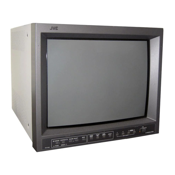
COLOR VIDEO MONITOR
TM-H150CG
TM-H150CG
TABLE OF CONTENTS
COPYRIGHT © 2004 VICTOR COMPANY OF JAPAN, LIMITED
,
/E
/U
BASIC CHASSIS
S1
No.YA068
2004/3
Advertisement
Chapters
Table of Contents

Related Manuals for JVC TM-H150CG/E


Summary of Contents for JVC TM-H150CG/E
- Page 1 SERVICE MANUAL COLOR VIDEO MONITOR YA068 2004 TM-H150CG TM-H150CG BASIC CHASSIS TABLE OF CONTENTS PRECAUTION............... . . 1-3 SPECIFIC SERVICE INSTRUCTIONS .
- Page 2 PAL / NTSC 3.58 Scanning Frequency H: 15.734 kHz (NTSC), 15.625 kHz (PAL) V: 59.94 Hz (NTSC), 50Hz (PAL) Power Requirements AC 220V-240V, 50Hz/60Hz [TM-H150CG/E] AC 120V, 50Hz/60Hz [TM-H150CG/U] High Voltage 23.7kV~26.3kV [at zero beam current] Power Consumption 0.8A [TM-H150CG/E] 1.2A [TM-H150CG/U]...
-
Page 3: Precaution
SECTION 1 PRECAUTION SAFETY PRECAUTIONS [EXCEPT FOR US and UK] (1) The design of this product contains special hardware, (8) When service is required, observe the original lead dress. many circuits and components specially for safety Extra precaution should be given to assure correct lead purposes. - Page 4 SAFETY PRECAUTIONS [FOR UK] (1) The design of this product contains special hardware and many circuits and components specially for safety purposes. For continued protection, no changes should be made to the original design unless authorized in writing by the manufacturer. Replacement parts must be identical to those used in the original circuits.
- Page 5 SAFETY PRECAUTIONS [FOR US] (1) The design of this product contains special hardware, many (10) Isolation Check (Safety for Electrical Shock Hazard) circuits and components specially for safety purposes. For After re-assembling the product, always perform an isolation continued protection, no changes should be made to the original check on the exposed metal parts of the cabinet (antenna design unless authorized in writing by the manufacturer.
-
Page 6: Specific Service Instructions
SECTION 2 SPECIFIC SERVICE INSTRUCTIONS FEATURES • High-resolution full square CRT is adopted. • It can respond to both NTSC and PAL signal system. The incoming signal was discriminated and the automatic selection function that changes the mode automatically is adopted. •... -
Page 7: Disassembly
SECTION 3 DISASSEMBLY DISASSEMBLY PROCEDURE CAUTION Even if the power switch is turned off, some parts in this unit are alive. Be sure to disconnect the power plug from the AC outlet before disassembly and reassembly. 3.1.1 REMOVING THE TOP COVER (1) Remove the 8 screws [A] as shown in Fig.4. - Page 8 LANDING COIL TOP COVER ( x 2) FRONT PANEL CRT SOCKET ( x 2) FRONT CONTROL DEG. COIL CHASSIS BASE SPEAKER DEF.PWB ( x 4) MAIN POWER SWITCH TERMINAL BRACKET EARTH WIRE ( x 1) MAIN PWB CONNECTOR AC INLET ( x 1) ( x 1) SIGNAL PWB...
- Page 9 3.1.4 REMOVING THE SLOT HOLDER AND SLOT PWB 3.1.8 CHECKING THE PW BOARD • Remove the TOP COVER. To check the PW board from back side. • Remove the REAR PANEL. (1) As shown in Fig.5, place the unit for service. •...
- Page 10 MEMORY IC REPLACEMENT 3.2.1 MEMORY IC This model uses memory IC. In the memory IC, there are <SET-UP MENU> memorized data for correctly operating for the video-chroma, deflection and the other control circuits. When replacing memory IC, be sure to use the IC written with the initial values of data.
- Page 11 3.2.3 FACTORY SETTING VALUE (USER MODE) INTIAL SETTING VALUE OF THE SET-UP MENU Setting item Setting content / Range Initial setting value CONTRAST -10 ~ 00 ~ +10 BRIGHT -10 ~ 00 ~ +10 PICTURE SUB ADJ. CHROMA -10 ~ 00 ~ +10 PHASE (NTSC) -10 ~ 00 ~ +10 H.
- Page 12 3.2.4 SERVICE MENU SETTING ITEMS (SERVICE MODE) SIGNAL BLOCK DEFLECTION BLOCK Item Contents Aspect ratio Vertical Item Contents Scan size frequency BRIGHT HORIZONTAL POSITION CONTRAST HORIZONTAL SIZE CHROMA(PAL) VERTICAL POSITION CHROMA(NTSC) VERTICAL SIZE PHASE(NTSC) NORMAL 50Hz VERTICAL LINEARITY SCAN CHROMA VERTICAL S-CORRECTION BRIGHT SIDEPIN PARABOLA...
- Page 13 REPLACEMENT OF CHIP COMPONENT 3.3.1 CAUTIONS (1) Avoid heating for more than 3 seconds. (2) Do not rub the electrodes and the resist parts of the pattern. (3) When removing a chip part, melt the solder adequately. (4) Do not reuse a chip part after removing it. 3.3.2 SOLDERING IRON (1) Use a high insulation soldering iron with a thin pointed end of it.
-
Page 14: Adjustment
SECTION 4 ADJUSTMENT ADJUSTMENT PREPARATION ADJUSTMENT ITEMS (1) There are 2 ways of adjusting this unit: One is with the CHECK ITEM MENU as On-Screen-Display and the other is the HIGH VOLTAGE check conventional method using adjustment parts and HIGH VOLTAGE HOLD DOWN check components. - Page 15 ADJUSTMENT LOCATIONS / WIRING DIAGRAM FRONT CONTROL PWB FRONT CHROMA MENU +(UP) (DOWN) /PHASE VOLUME/SELECT ASPECT COLOR POWER SW SLOT VIDEO CONTRAST BLUE UNDER /BRIGHT CHECK SCAN SUB DEF. PWB CN2004 FRONT 1pin :NC 2pin :NC 3pin :X-RAY2 4pin :X-RAY1 5pin :TP-E(GND ) 6pin :NC CN2003...
- Page 16 CRT SOCKET PWB SLOT PWB (SOLDER SIDE) CRT EARTH WIRE CN8006 (50pin) (BRAIDED ASS'Y) TP-47B CN8005 TP-E TP-47G COMPONENT/RGB INPUT CARD MAIN PWB (OPTION) LANDING COIL (canceller) SIGNAL PWB FRONT CN6005 IC6701 MICRO COMPUTER IC6702 MEMORY IC CN6002 CN6001 1-16 (No.YA068)
- Page 17 BASIC OPERATION OF SERVICE MENU 4.7.1 SERVICE MENU ITEMS With the SERVICE MENU, various settings can be made, and they are broadly classified in the following items of adjustments. • It is no requirement for adjustment portion of the DEFLECTION BLOCK and CONTROL BLOCK This block adjusts the data of the SIGNAL BLOCK various signal circuit controls.
- Page 18 4.7.4 OPERATION OF < BLOCK SELECT > SCREEN While the SERVICE MENU < BLOCK SELECT > screen is displaying, in accordance with (FUNCTION DISPLAY) at the lower side of the screen, be able to operate the various items (Fig. 7). <...
- Page 19 4.7.6 SERVICE MENU ITEMS SIGNAL BLOCK Item No. Setting value SIGNAL BLOCK < FUNCTION DISPLAY > <S01> : EXIT DISP EXIT DISP <S01>: Display on/off button Fig.9 Item No. Setting value Exit button select button (+/-) button <FRONT PANEL BUTTON> WHITE BALANCE BLOCK WHITE BALANCE BLOCK <...
- Page 20 [ WHITE BALANCE ADJUSTMENT : METHOD 1 ] • Accordance with the screen display, select the each WHITE BALANCE mode following below. • Refer to the "Low-Light adjustment" corresponding page about detailed adjustment steps. CUTOFF ADJUSTMENT MODE (LOW LIGHT ADJUSTMENT) Setting value CUTOFF ADJUSTMENT MODE Contents...
- Page 21 DEFLECTION BLOCK DEFLECTION BLOCK Setting value Item No. < FUNCTION DISPLAY > <D01> : EXIT EXIT <D01 > : Fig.14 Item No. Setting value Exit button select button (+/-) button <FRONT PANEL BUTTON> CONTROL BLOCK Item No. Setting value CONTROL BLOCK <...
- Page 22 4.7.7 SERVICE MENU FLOW CHART SERVICE MENU <BLOCK SELECT> SCREEN < BLOCK SELECT > SIGNAL BLOCK WHITE BALANCE BLOCK DEFLECTION BLOCK CONTROL BLOCK DEF CTRL EXIT SIGNAL BLOCK CUTOFF ADJUSTMENT EXIT DISP <S01>: R CUTOFF : RGB SERV EXIT WHITE BALANCE BLOCK MENU SCREEN DRIVE ADJUSTMENT <...
- Page 23 INITIAL SETTING VALUE OF SERVICE MENU It is no requirement for adjustment of the part of the tables. Don' t change the values. [SIGNAL BLOCK] Item Input signal Contents Variable range Initial value BRIGHT 000 ~ 255 CONTRAST 000 ~ 127 VIDEO CHROMA(PAL) 000 ~ 127...
- Page 24 [DEFLECTION BLOCK] Aspect ratio/ Vertical Item Contents Variable range Initial value Scan size frequency HORIZONTAL POSITION 000 ~ 031 HORIZONTAL SIZE 000 ~ 063 VERTICAL POSITION 000 ~ 127 VERTICAL SIZE 000 ~ 127 50Hz NORMAL VERTICAL LINEARITY 000 ~ 031 VERTICAL S-CORRECTION 000 ~ 063 SIDEPIN PARABOLA...
- Page 25 [CONTROL BLOCK] Item. Contents Variable range Initial value DESTINATION 000 ~ 129 001(US/EU) UPPER 000 ~ 255 BRIGHT POINT LOWER 000 ~ 255 UPPER 000 ~ 127 CONTRAST POINT LOWER 000 ~ 127 UPPER 000 ~ 127 CHROMA POINT LOWER 000 ~ 127 UPPER 000 ~ 127...
- Page 26 4.10 ADJUSTMENT PROCEDURE 4.10.1 CHECK ITEM Measuring Item Test points Adjustment part Description instrument HIGH HV voltmeter CRT anode SCREEN VR (1) Receive a whole black signal. VOLTAGE [in FBT] (2) Connect the HV voltmeter to the CRT anode and check check it as 25.0kV±1.3kV.
- Page 27 4.10.2 B1 VOLTAGE Measuring Item Test points Adjustment part Description instrument B1 VOLTAGE Signal TP-B1 B1 ADJ VR (1) Receive a whole black signal. generator (VR1901) (2) Connect a DC voltmeter to TP-B1 and TP-E( ). TP-E(GND) [MAIN PWB] (3) Adjust the B1 ADJ VR(VR1901) so that B1 voltage is DC voltmeter (E2) at 53V±0.2V.
- Page 28 4.10.4 VIDEO CIRCUIT When you perform WHITE BALANCE adjustment, be sure to input a video composite signal. Moreover, set the aspect ratio to 4:3. It is no requirement to adjust in 16:9 mode. Measuring Item Test points Adjustment part Description instrument WHITE Signal...
- Page 29 Measuring Item Test points Adjustment part Description instrument 6500K WHITE Signal [WHITE BALANCE • Check the LOW LIGHT adjustment has been finished BALANCE generator BLOCK] correctly before performing HIGH LIGHT adjustment. HIGH LIGHT W04 : R DRIVE (1) Input the gray scale signal. Color W05 : B DRIVE (2) Select the WHITE BALANCE BLOCK mode with...
- Page 30 Measuring Item Test points Adjustment part Description instrument BRIGHT Signal [SIGNAL BLOCK] • Under the condition that LOW LIGHT adjustment has generator S01 : BRIGHT been correctly finished. (1) Input the gray scale signal. (2) Select the SIGNAL BLOCK with [CHROMA / PHASE] button (<...
- Page 31 Measuring Item Test points Adjustment part Adjustment procedure instrument PAL CHROMA Signa TP-47B [SIGNAL BLOCK] (1) Input the PAL color bar signal (75% white). generator TP-E S03 : PAL CHROMA (2) Connect the oscilloscope to TP-47B and TP-E. [CRT SOCKET (3) Select the SIGNAL BLOCK with [CHROMA/PHASE] Oscilloscope PWB]...
- Page 32 Measuring Item Test points Adjustment part Adjustment procedure instrument NTSC PHASE Signal TP-47B [SIGNAL BLOCK] (1) Input the NTSC color bar signal (75% white). generator TP-E S05: NTSC PHASE (2) Connect the oscilloscope to TP-47B and TP-E. [CRT SOCKET (3) Select the SIGNAL BLOCK with [CHROMA/PHASE] Oscilloscope PWB] button (<...
- Page 33 Measuring Item Test points Adjustment part Adjustment procedure instrument RGB BRIGHT Component / [SIGNAL BLOCK] (1) Input the whole black signal to the each terminal of RGB input S07 : RGB BRIGHT the Component / RGB input card. card (2) In case of using the composite sync. signal, input the (IF-C01COMG) sync.
- Page 34 4.10.5 DEFLECTION CIRCUIT There are 2 kind of adjustment for the DEFLECTION circuit, PAL and NTSC. The adjustment using PAL signal is as the standard of all DEFLECTION adjustment. The "#" mark in the table given below expresses the number of each adjustment item. The screen aspect ratio 4 : 3 at 50Hz (PAL) is regarded as the reference value for all adjustments.
- Page 35 Measuring Item Test points Adjustment part Adjustment procedure instrument V. POSITION Signal [DEFLECTION BLOCK] (1) Input the PAL circle pattern signal. generator D03 : V. POSITION (2) Adjust < D03 >(V. POSITION) to agree with CRT center and signal center of vertical direction. V.
- Page 36 Measuring Item Test points Adjustment part Adjustment procedure instrument Signal [DEFLECTION (1) Input the PAL crosshatch signal. V. SIZE generator BLOCK] (2) Adjust < D04 >(V. SIZE) to become the vertical scan D04 : V.SIZE size to 95%. Screen size Picture size 100% 16:9...
- Page 37 Measuring Item Test points Adjustment part Adjustment procedure instrument UNDERSCAN Signal [DEFLECTION (1) Input the PAL circle pattern signal. H. POSITION / generator BLOCK] (2) Select the aspect ratio to the 4:3 mode. H. SIZE DD1 : H. CENTER (3) Select the underscan mode to ON. DD2 : H.
-
Page 38: Trouble Shooting
SECTION 5 TROUBLE SHOOTING OUTLINE This model includes a SELF DIAGNOSIS FUNCTION that checks the circuit operating status and in event of malfunction, displays and stores the data in a memory. The data are stored in memory. Fault detection starts with the I C bus and is performed according to the input states of the control lines connected to the MAIN CPU. - Page 39 TM-H150CG TM-H150CG STANDARD CIRCUIT DIAGRAM NOTE ON USING CIRCUIT DIAGRAMS 1.SAFETY Type No indication : Ceramic capacitor The components identified by the symbol and shading are : Metalized mylar capacitor critical for safety. For continued safety replace safety ciritical : Polypropylene capacitor components only with manufactures recommended parts.
-
Page 40: Table Of Contents
CONTENTS SEMICONDUCTOR SHAPES ..............2-2 BLOCK DIAGRAM ..................2-3 CIRCUIT DIAGRAMS ..................2-5 SIGNAL PWB CIRCUIT DIAGRAM ......................2-5 MAIN PWB CIRCUIT DIAGRAM ........................ 2-9 SUB DEF PWB CIRCUIT DIAGRAM ......................2-13 CRT SOCKET PWB CIRCUIT DIAGRAM ....................2-15 FRONT CONTROL PWB CIRCUIT DIAGRAM ..................2-17 SLOT PWB CIRCUIT DIAGRAM ...................... -
Page 41: Block Diagram
BLOCK DIAGRAM G/Y,R/R-Y,B/B-Y SLOT PWB SYNC SYNC IC6201 IC6602 CS/HD VIDEO A IC6101 PAL 1H DELAY INT/SLOT SW IC8001 VIDEO COMB VIDEO B SYNC R/R-Y FILTER B/B-Y MIXER x0.5 SLOT IC8002 CONNECTOR Y IN Q3301 R/G/B G/Y,R/R-Y,B/B-Y DELAY Q3302 IC6102 VIDEO SW R/G/B AUDIO... -
Page 42: Circuit Diagrams
CIRCUIT DIAGRAMS SIGNAL PWB CIRCUIT DIAGRAM (1/2) LANDING COIL NOT USE CN600R CN60S3 QGA2501F1-03 QGA2501F1-03 MODE MODE MODE MODE R6063 DC (V) DC (V) DC (V) DC (V) IC6904 R6785 D6034 PIN NO. PIN NO. PIN NO. PIN NO. C6041 AN78L05-T R6064 C6002... -
Page 43: Signal Pwb Circuit Diagram
SIGNAL PWB CIRCUIT DIAGRAM (2/2) IC6701 - 30 IC6701 - 31 IC6701 - 62 IC6701 - 63 MODE MODE MODE DC (V) DC (V) DC (V) PIN NO. PIN NO. PIN NO. IC6701 IC6802 Q6718 11.6 11.6 11.9 Q6705 -0.2 11.5 11.6 Q6704... -
Page 44: Main Pwb Circuit Diagram
MAIN PWB CIRCUIT DIAGRAM (1/2) MODE MODE DC (V) DC (V) PIN NO. PIN NO. IC1401 - 3,6 Q1501 - G Q1501 - D Q1521 - B Q1521 - C T1551 - 5 T1551 - 6 IC1401 - 1,7 IC1401 - 5 T1551 - 4 T1551 - 7 IC1451 - 1... - Page 45 K1402 R1567 R1452 OPEN E/W.OUT R1428 V.DRIVE SCAN X.RAY B1.PROT V.CUTOFF H.OUT DEG.SW SCL1 SDA1 VHSS PW_STB PW_MAIN INPUT_D INPUT_C INPUT_B INPUT_A ASPECT B.CHK C.OFF U.SCAN KEY1 KEY5 KEY2 VOLUME KEY3 MUTE KEY4 AUDIO KEY4 KEY3 KEY2 KEY5 KEY1 U.SCAN C.OFF B.CHK ASPECT...
-
Page 46: Sub Def Pwb Circuit Diagram
SUB DEF PWB CIRCUIT DIAGRAM MAIN PWB(1/2) MAIN PWB(1/2) CN2003 CN2004 QGBA001J1-04 QGBA001J1-04 GND2 L2552 C2522 .012 QQL50AM-8R2Z QFZ0196-123 R2572 15.8k 1/4W R2525 C2528 .0025 QRA14CF-1582Y OMR2 R2462 R2461 QFZ0196-252 R2522 QRX029J-8R2 QRG039J-680 QRG039J-680 C2525 /160 L2461 D2523 QQR1451-001 C2521 .002 D2521 D2522... -
Page 47: Crt Socket Pwb Circuit Diagram
CRT SOCKET PWB CIRCUIT DIAGRAM L3301 Q3301 - C Q3302 - C Q3303 - C R3312 QQL244J-151Z R3313 R3304 R3311 Q3303 2SC4544-LB QRZ0111-102 C3316 220p TP-47G TP-47B R3320 GND2 Q3306 2SC3311A/QR/-T C3312 R3332 1.5k R3329 C3313 270p R3330 R3331 CN300T R3338 QGA2501C1-10 L3302... - Page 48 PW_MAIN INPUT_D INPUT_C INPUT_B INPUT_A ASPECT B.CHK PW_STB PW_MAIN INPUT_D C.OFF INPUT_C INPUT_B INPUT_A ASPECT B.CHK C.OFF U.SCAN KEY1 KEY5 U.SCAN KEY2 KEY3 KEY4...
-
Page 49: Slot Pwb Circuit Diagram
SLOT PWB CIRCUIT DIAGRAM MODE DC (V) PIN NO. CN8006 QGB2514J1-50 CN8005 IC8001 QGB1505K1-25 R8027 Q8005 3.3K R8005 R8028 3.3K 3.3K R8001 IC8001 C8013 Q8001 Q8004 TC74VHC86F-X R8006 R8013 C8012 5.6k C8001 IC8002 C8014 D8001 R8010 C8016 Q8003 R8035 R8023 150k SIGNAL PWB R8011... -
Page 50: Pattern Diagrams
PATTERN DIAGRAMS MAIN PWB PATTERN R1563 W1402 W1415 W1213 D1404 R1428 D1403 C1458 C1451 H1003 Q1551 R1560 R1564 C1611 Q1451 C1413 C1408 C1619 R1972 Q1603 R1562 Q1405 D1556 IC1401 C1412 C1605 C1454 C1424 C1603 C1615 C1994 CP1971 R1453 W1231 W1230 R1567 R1433 D1605... -
Page 51: Signal Pwb Pattern
SIGNAL PWB PATTERN CL6001 R6648 W6128 C6042 R6064 R6765 D6707 R6073 R6767 R6766 R6070 Q6509 D6706 W6126 R6768 R6540 R6074 Q6708 R6071 W6275 R6770 W6123 R6543 R6541 IC6004 R6072 Q6707 C6712 C6711 W6481 R6797 W6129 R6057 D6512 W6272 W6269 W6357 D6514 D6513 C6704... -
Page 52: Front Control Pwb Pattern
FRONT CONTROL PWB PATTERN D4801 S4814 S4813 S4808 S4807 S4806 S4805 S4804 S4803 S4802 S4801 S4812 S4811 S4810 S4809 D4809 D4808 D4807 D4806 D4805 D4804 D4803 D4802 R4809 R4807 R4801 R4806 R4803 R4810 R4811 R4808 R4805 R4804 R4802 R4812 SLOT PWB PATTERN W8105 C8016 D8005... -
Page 53: Crt Socket Pwb Pattern
CRT SOCKET PWB PATTERN C3308 C3313 R3323 R3329 R3321 W3202 C3301 C3309 R3330 R3340 C3303 R3324 R3302 C3316 R3337 C3311 R3335 C3314 R3327 R3326 R3325 C3310 TP-47B R3341 Q3305 W3403 C3315 R3328 TP-E Q3302 R3339 L3301 R3303 R3308 TP-47G R3317 SK3001 L3302 D3301... -
Page 54: Sub Def Pwb Pattern
SUB DEF PWB PATTERN CL2001 CL2002 CL2003 C2525 D2522 L2461 C2520 C2453 R2573 R2572 C2528 C2524 C2522 C2521 D2521 W2701 CN2004 CN2003 No.YA068 2-28... -
Page 55: Parts List
PARTS LIST CAUTION The parts identified by the symbol are important for the safety . Whenever replacing these parts, be sure to use specified ones to secure the safety. The parts not indicated in this Parts List and those which are filled with lines --- in the Parts No. columns will not be supplied. P.W. - Page 56 CONTENTS USING P.W. BOARD & REMOTE CONTROL UNIT ....................3-2 EXPLODED VIEW PARTS LIST -1 ..........................3-3 EXPLODED VIEW -1 ..............................3-3 EXPLODED VIEW PARTS LIST -2 ..........................3-4 EXPLODED VIEW -2 ..............................3-5 PRINTED WIRING BOARD PARTS LIST MAIN P.W. BOARD ASS'Y (FX-1187A-H2) ....................... 3-6 SUB DEF P.W.
-
Page 57: Exploded View Parts List -1
EXPLODED VIEW PARTS LIST -1 Ref.No. Part No. Part Name Description Local LC11757-001A-H FRONT PANEL CM48149-A01 JVC MARK LC21470-001A-H CONTROL SHEET EXPLODED VIEW -1 (No.YA068)3-3... -
Page 58: Exploded View Parts List -2
EXPLODED VIEW PARTS LIST -2 Ref.No. Part No. Part Name Description Local V01 M36AES13X01/L/ Inc.DEF YOKE/PC MAGNET/WEDGE L01 QQW0186-001 DEG COIL T1551 QQH0178-001 FB TRANSF LC31575-001B-H PUSH KNOB (x4) QQW0185-001 CANCELLER COIL WJY0027-001A BRAIDED ASSY CHFD119-14BD FFC WIRE CEBSS08P-01KJ2... -
Page 59: Exploded View -2
EXPLODED VIEW -2 FRONT PANEL T1551 MAIN POWER TERMINAL SWITCH BRACKET EARTH WIRE CONNECTOR AC INLET SLOT HOLDER POWER CORD (No.YA068)3-5... -
Page 60: Printed Wiring Board Parts List
PRINTED WIRING BOARD PARTS LIST MAIN P.W. BOARD ASS'Y (FX-1187A-H2) Ref No. Part No. Part Name Description Local Ref No. Part No. Part Name Description Local D1941 MTZJ7.5S-T2 Z DIODE D1942 1SS133-T2 DIODE IC1401 LA78041 D1943 1SS133-T2 DIODE IC1411 TA1241AN D1971 RU30-F1 SI DIODE... - Page 61 Ref No. Part No. Part Name Description Local Ref No. Part No. Part Name Description Local C1912 QEHR1HM-476Z E CAPACITOR 47uF 50V M R1552 QRZ9024-R82 FUSIBLE RESISTO 0.82Ω 2W K C1914 QCB31HK-102Z C CAPACITOR 1000pF 50V K QRZ9024-R82 FUSIBLE RESISTO 0.82Ω...
-
Page 62: Sub Def P.w. Board Ass'y (Fx-2095A-H2)
Ref No. Part No. Part Name Description Local Ref No. Part No. Part Name Description Local L1974 QQL26AK-560Z CHOKE COIL 56uH K Q3305 2SC3311A/QR/-T TRANSISTOR T1501 QQR1032-001 HOR DRIVE TRANS Q3306 2SC3311A/QR/-T TRANSISTOR T1901 QQS0257-001 SW TRANSF Q3307 2SC3311A/QR/-T TRANSISTOR QQS0130-001 SW TRANSF T1902... -
Page 63: Signal P.w. Board Ass'y (Fx-6143A-H2)
Ref No. Part No. Part Name Description Local Ref No. Part No. Part Name Description Local R4801 QRE141J-562Y C RESISTOR 5.6kΩ 1/4W J Q6509 2SC3928A/QR/-X TRANSISTOR R4802 QRE141J-332Y C RESISTOR 3.3kΩ 1/4W J Q6510 DTC124EKA-X DIGI TRANSISTOR R4803 QRE141J-562Y C RESISTOR 5.6kΩ... - Page 64 Ref No. Part No. Part Name Description Local Ref No. Part No. Part Name Description Local D6520 MA3068/M/-X Z DIODE C6136 NDC31HJ-181X C CAPACITOR 180pF 50V J D6702 MA111-X SI DIODE C6137 NDC31HJ-181X C CAPACITOR 180pF 50V J D6703 MA111-X SI DIODE C6141 QTNC1CM-106Z...
- Page 65 Ref No. Part No. Part Name Description Local Ref No. Part No. Part Name Description Local C6708 NCB31CK-104X C CAPACITOR 0.1uF 16V K R6102 NRSA63J-332X MG RESISTOR 3.3kΩ 1/16W J C6709 QEHR1EM-227Z E CAPACITOR 220uF 25V M R6103 NRSA63J-102X MG RESISTOR 1kΩ...
- Page 66 Ref No. Part No. Part Name Description Local Ref No. Part No. Part Name Description Local R6504 NRSA63J-272X MG RESISTOR 2.7kΩ 1/16W J R6717 NRSA63J-103X MG RESISTOR 10kΩ 1/16W J R6505 NRSA63J-391X MG RESISTOR 390Ω 1/16W J R6718 NRSA63J-391X MG RESISTOR 390Ω...
-
Page 67: Slot P.w. Board Ass'y (Fx-8033A-H2)
Ref No. Part No. Part Name Description Local Ref No. Part No. Part Name Description Local R6812 NRVA02D-102X CMF RESISTOR 1kΩ 1/10W D C8014 QEHR1CM-107Z E CAPACITOR 100uF 16V M R6814 NRVA02D-682X CMF RESISTOR 6.8kΩ 1/10W D C8015 NCB31CK-104X C CAPACITOR 0.1uF 16V K R6815 NRSA63J-104X... -
Page 68: Packing
PACKING PACKING PARTS LIST Ref.No. Part No. Part Name Description Local LC11194-021A-H PACKING CASE LVL-TMH150CGE CORNER LABEL (x2) TM-H150CG/E LVL-TMH150CGU CORNER LABEL (x2) TM-H150CG/U LC11760-002A-H CUSHION ASSY 4pcs in 1set CP30967-003-H POLY BAG QPA01203005 POLY BAG 12cm x 30cm TM-H150CG/U ... - Page 69 VICTOR COMPANY OF JAPAN, LIMITED AV & MULTIMEDIA COMPANY VIDEO DISPLAY CATEGORY 12, 3-chome, Moriya-cho, kanagawa-ku, Yokohama, kanagawa-prefecture, 221-8528, Japan (No.YA068) Printed in Japan...