Table of Contents
Advertisement
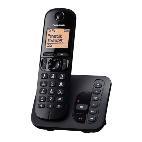
Caller ID Compatible
KX-TGCA20
(Handset)
KX-TGC220
(Base Unit)
Configuration for each model
Model No
Base Unit
KX-TGC210
1 (TGC210) 1 (TGCA20)
KX-TGC212
1 (TGC210) 2 (TGCA20)
KX-TGC213
1 (TGC210) 3 (TGCA20)
KX-TGC220
1 (TGC220) 1 (TGCA20)
KX-TGC222
1 (TGC220) 2 (TGCA20)
KX-TGC223
1 (TGC220) 3 (TGCA20)
KX-TGCA20
KX-TGC210
(Base Unit)
(Charger Unit)
Handset Charger Unit
1
2
1
2
1 (TGCA20)
1
Telephone Equipment
KX-TGC210LAB
Model No.
KX-TGC212LAB
KX-TGC213LAB
KX-TGC220LAB
KX-TGC222LAB
KX-TGC223LAB
KX-TGCA20LAB
Digital Cordless Phone
Digital Cordless Answering System
B: Black Version
(for Latin America)
© Panasonic System Networks Co., Ltd. 2014
Unauthorized copying and distribution is a violation
of law.
ORDER NO. KM41404824CE
Advertisement
Table of Contents

Related Manuals for Panasonic KX-TGC210LAB


Summary of Contents for Panasonic KX-TGC210LAB
- Page 1 1 (TGC210) 2 (TGCA20) KX-TGC213 1 (TGC210) 3 (TGCA20) KX-TGC220 1 (TGC220) 1 (TGCA20) KX-TGC222 1 (TGC220) 2 (TGCA20) KX-TGC223 1 (TGC220) 3 (TGCA20) KX-TGCA20 1 (TGCA20) © Panasonic System Networks Co., Ltd. 2014 Unauthorized copying and distribution is a violation of law.
- Page 2 KX-TGC210LAB/KX-TGC212LAB/KX-TGC213LAB/KX-TGC220LAB/KX-TGC222LAB/KX-TGC223LAB/KX-TGCA20LAB WARNING This service information is designed for experienced repair technicians only and is not designed for use by the general public. It does not contain warnings or cautions to advise non-technical individuals of potential dangers in attempting to service a product. Products powered by electricity should be serviced or repaired only by experienced professional technicians.
-
Page 3: Table Of Contents
KX-TGC210LAB/KX-TGC212LAB/KX-TGC213LAB/KX-TGC220LAB/KX-TGC222LAB/KX-TGC223LAB/KX-TGCA20LAB TABLE OF CONTENTS PAGE PAGE 1 Safety Precautions----------------------------------------------- 5 11.1.1. Base Unit ---------------------------------------------- 41 1.1. For Service Technicians --------------------------------- 5 11.1.2. Handset ------------------------------------------------ 44 2 Warning -------------------------------------------------------------- 5 11.1.3. Charger Unit ------------------------------------------ 45 2.1. Battery Caution--------------------------------------------- 5 11.2. How to Replace the Handset LCD------------------- 46 12 Measurements and Adjustments -------------------------- 47 2.2. - Page 4 KX-TGC210LAB/KX-TGC212LAB/KX-TGC213LAB/KX-TGC220LAB/KX-TGC222LAB/KX-TGC223LAB/KX-TGCA20LAB 16.5. Replacement Parts List --------------------------------- 85 16.5.1. Base Unit ---------------------------------------------- 85 16.5.2. Handset ------------------------------------------------ 87 16.5.3. Charger Unit ------------------------------------------ 88 16.5.4. Accessories and Packing Materials------------- 88 16.5.5. Screws ------------------------------------------------- 89 16.5.6. Fixtures and Tools----------------------------------- 89...
-
Page 5: Safety Precautions
KX-TGC210LAB/KX-TGC212LAB/KX-TGC213LAB/KX-TGC220LAB/KX-TGC222LAB/KX-TGC223LAB/KX-TGCA20LAB 1 Safety Precautions 1.1. For Service Technicians • Repair service shall be provided in accordance with repair technology information such as service manual so as to prevent fires, injury or electric shock, which can be caused by improper repair work. -
Page 6: Suggested Pbf Solder
KX-TGC210LAB/KX-TGC212LAB/KX-TGC213LAB/KX-TGC220LAB/KX-TGC222LAB/KX-TGC223LAB/KX-TGCA20LAB 2.2.1. Suggested PbF Solder There are several types of PbF solder available commercially. While this product is manufactured using Tin, Silver, and Copper (Sn+Ag+Cu), you can also use Tin and Copper (Sn+Cu), or Tin, Zinc, and Bismuth (Sn+Zn+Bi). Please check the manufacturer's specific instructions for the melting points of their products and any precautions for using their product with other materials. -
Page 7: Specifications
KX-TGC210LAB/KX-TGC212LAB/KX-TGC213LAB/KX-TGC220LAB/KX-TGC222LAB/KX-TGC223LAB/KX-TGCA20LAB 3 Specifications Standard: Bit rate: DECT 6.0 (Digital Enhanced Cordless 1,152 kbit/s Telecommunications 6.0) Modulation: Number of channels: GFSK (Gaussian Frequency Shift Keying) 120 Duplex Channels RF transmission power: Frequency range: 115 mW (max.) 1.91 GHz to 1.93 GHz... -
Page 8: Technical Descriptions
KX-TGC210LAB/KX-TGC212LAB/KX-TGC213LAB/KX-TGC220LAB/KX-TGC222LAB/KX-TGC223LAB/KX-TGCA20LAB 4 Technical Descriptions 4.1. US-DECT Description The frequency range of 1.92 GHz-1.93 GHz is used. Transmitting and receiving carrier between base unit and handset is same frequency. Refer to Frequency Table (P.54). 4.1.1. TDD Frame Format 5 ms 5 ms Up Link ( Handset - >... -
Page 9: Signal Flowchart In The Radio Parts
KX-TGC210LAB/KX-TGC212LAB/KX-TGC213LAB/KX-TGC220LAB/KX-TGC222LAB/KX-TGC223LAB/KX-TGCA20LAB 4.1.3. Signal Flowchart in the Radio Parts Reception A voice signal from TEL line is encoded to digital data "TXDATA" by BBIC (IC501) in a base unit. Then TXDATA goes to RF PART and it's modulated to 1.9 GHz. The RF signal is amplified and fed to a selected antenna. -
Page 10: Block Diagram (Base Unit_Main)
KX-TGC210LAB/KX-TGC212LAB/KX-TGC213LAB/KX-TGC220LAB/KX-TGC222LAB/KX-TGC223LAB/KX-TGCA20LAB 4.2. Block Diagram (Base Unit_Main) -
Page 11: Block Diagram (Base Unit_Rf Part)
KX-TGC210LAB/KX-TGC212LAB/KX-TGC213LAB/KX-TGC220LAB/KX-TGC222LAB/KX-TGC223LAB/KX-TGCA20LAB 4.3. Block Diagram (Base Unit_RF Part) ANT1 KX-TGC210/212/213/220/222/223 BLOCK DIAGRAM (Base Unit_RF Part) -
Page 12: Circuit Operation (Base Unit)
KX-TGC210LAB/KX-TGC212LAB/KX-TGC213LAB/KX-TGC220LAB/KX-TGC222LAB/KX-TGC223LAB/KX-TGCA20LAB 4.4. Circuit Operation (Base Unit) General Description: (BBIC, Flash Memory, EERROM) is a digital speech/signal processing system that implements all the functions of speech compression, record and playback, and memory management required in a digital telephone answering machine. The BBIC system is fully controlled by a host processor. The host processor provides activation and control of all that functions as follows. -
Page 13: Power Supply Circuit/Reset Circuit
KX-TGC210LAB/KX-TGC212LAB/KX-TGC213LAB/KX-TGC220LAB/KX-TGC222LAB/KX-TGC223LAB/KX-TGCA20LAB 4.4.4. Power Supply Circuit/Reset Circuit The power supply voltage from AC adaptor is converted to VBAT (3.0V) in IC302. And +3.0V for peripherals and analog part is insulated from VBAT by Doubler of BBIC. Circuit Operation: +3.0V VBAT IC601... - Page 14 KX-TGC210LAB/KX-TGC212LAB/KX-TGC213LAB/KX-TGC220LAB/KX-TGC222LAB/KX-TGC223LAB/KX-TGCA20LAB 4.4.4.1. Charge Circuit The voltage from the AC adaptor is supplied to the charge circuits. +5.5V F301 CHARGE+ CHARGE-...
-
Page 15: Telephone Line Interface
KX-TGC210LAB/KX-TGC212LAB/KX-TGC213LAB/KX-TGC220LAB/KX-TGC222LAB/KX-TGC223LAB/KX-TGCA20LAB 4.4.5. Telephone Line Interface Telephone Line Interface Circuit: Function • Bell signal detection • ON/OFF hook and pulse dial circuit • Side tone circuit Bell signal detection and OFF HOOK circuit: In the idle mode, Q141 is open to cut the DC loop current and decrease the ring load. When ring voltage appears at the Tip (T) and Ring (R) leads (When the telephone rings), the AC ring voltage is transferred as follows: T ... - Page 16 KX-TGC210LAB/KX-TGC212LAB/KX-TGC213LAB/KX-TGC220LAB/KX-TGC222LAB/KX-TGC223LAB/KX-TGCA20LAB detecting the voltage changes. If the Auto disconnect function is ON and statuses are Hold, receiving ICM, OGM transmitting, BBIC disconnects the line after detecting parallel connection is off hook. Q141 Q161 C101 Pin 18 of IC501 DCIN2 D101...
-
Page 17: Calling Line Identification (Caller Id)/Call Waiting Caller
KX-TGC210LAB/KX-TGC212LAB/KX-TGC213LAB/KX-TGC220LAB/KX-TGC222LAB/KX-TGC223LAB/KX-TGCA20LAB 4.4.7. Calling Line Identification (Caller ID)/Call Waiting Caller ID Function: Caller ID The caller ID is a chargeable ID which the user of a telephone circuit obtains by entering a contract with the telephone company to utilize a caller ID service. For this reason, the operation of this circuit assumes that a caller ID service contract has been entered for the circuit being used. - Page 18 KX-TGC210LAB/KX-TGC212LAB/KX-TGC213LAB/KX-TGC220LAB/KX-TGC222LAB/KX-TGC223LAB/KX-TGCA20LAB Call Waiting Caller ID Calling Identity Delivery on Call Waiting (CIDCW) is a CLASS service that allows a customer, while off-hook on an existing call, to receive information about a calling party on a waited call. The transmission of the calling information takes place almost immediately after the customer is alerted to the new call so he/she can use this information to decide whether to take the new call.
-
Page 19: Block Diagram (Handset)
KX-TGC210LAB/KX-TGC212LAB/KX-TGC213LAB/KX-TGC220LAB/KX-TGC222LAB/KX-TGC223LAB/KX-TGCA20LAB 4.5. Block Diagram (Handset) -
Page 20: Circuit Operation (Handset)
KX-TGC210LAB/KX-TGC212LAB/KX-TGC213LAB/KX-TGC220LAB/KX-TGC222LAB/KX-TGC223LAB/KX-TGCA20LAB 4.6. Circuit Operation (Handset) 4.6.1. Outline Handset consists of the following ICs as shown in Block Diagram (Handset) (P.19). • DECT BBIC (Base Band IC): IC1 - All data signals (forming/analyzing ACK or CMD signal) - All interfaces (ex: Key, Detector Circuit, Charge, DC/DC Converter, EEPROM, LCD, RF Power Amp.) -
Page 21: Signal Route
KX-TGC210LAB/KX-TGC212LAB/KX-TGC213LAB/KX-TGC220LAB/KX-TGC222LAB/KX-TGC223LAB/KX-TGCA20LAB 4.7. Signal Route SIGNAL ROUTE ROUTE HANDSET TX MIC (+) - C13 - IC1 (17) IC1(86) C859 - ANT to BASE MIC (–) - C11 - IC1 (18) IC1(87) ---ANT. - <BASE_UNIT_RF_RX_ROUTE> - IC501(46/47 - 28) - C184 - Q161 - Q141... - Page 22 KX-TGC210LAB/KX-TGC212LAB/KX-TGC213LAB/KX-TGC220LAB/KX-TGC222LAB/KX-TGC223LAB/KX-TGCA20LAB RF part signal route SIGNAL ROUTE ROUTE HANDSET RF IC1(86/87) - C859 - ANT [ TX_ROUTE ] HANDSET RF ANT - IC(1/2) [ RX_ROUTE ] IC501(44/45) - C819 - C872 - ANT BASE UNIT RF [ TX_ROUTE ] ANT - C872 - C895 - IC501(46/47)
-
Page 23: Location Of Controls And Components
KX-TGC210LAB/KX-TGC212LAB/KX-TGC213LAB/KX-TGC220LAB/KX-TGC222LAB/KX-TGC223LAB/KX-TGCA20LAB 5 Location of Controls and Components Refer to the Operating Instructions. Note: You can download and refer to the Operating Instructions (Instruction book) on TSN Server. 6 Installation Instructions Refer to the Operating Instructions. Note: You can download and refer to the Operating Instructions (Instruction book) on TSN Server. -
Page 24: Test Mode
KX-TGC210LAB/KX-TGC212LAB/KX-TGC213LAB/KX-TGC220LAB/KX-TGC222LAB/KX-TGC223LAB/KX-TGCA20LAB 8 Test Mode 8.1. Engineering Mode 8.1.1. Base Unit Important: Make sure the address on LCD is correct when entering new data. Otherwise, you may ruin the unit. Soft keys { OFF } (Off) Navigator key/ (Volume) key/ (Phonebook)/... - Page 25 KX-TGC210LAB/KX-TGC212LAB/KX-TGC213LAB/KX-TGC220LAB/KX-TGC222LAB/KX-TGC223LAB/KX-TGCA20LAB Frequently Used Items (Base Unit) ex.) Items Address Default Data New Data Remarks C-ID (FSK) sensitivity 06 DD/06 DC 00/28 00/1C 00/14 When hex changes from “00/28” to “00/1C” or (3 dB up) (6 dB up) “00/14”, gain increases by 3 dB or 6 dB.
-
Page 26: Handset
KX-TGC210LAB/KX-TGC212LAB/KX-TGC213LAB/KX-TGC220LAB/KX-TGC222LAB/KX-TGC223LAB/KX-TGCA20LAB 8.1.2. Handset Important: Make sure the address on LCD is correct when entering new data. Otherwise, you may ruin the unit. Soft keys { OFF } (Off) Navigator key/ (Volume) key/ (Phonebook)/ CID (Caller ID) key/ REDIAL (Redial) key/... - Page 27 KX-TGC210LAB/KX-TGC212LAB/KX-TGC213LAB/KX-TGC220LAB/KX-TGC222LAB/KX-TGC223LAB/KX-TGCA20LAB Frequently Used Items (Handset) ex.) Items Address Default Data New Data Possible Adjusted Possible Adjusted Remarks Value MAX (hex) Value MIN (hex) Battery Low 00 09 (*2) Frequency 00 07 / 00 08 70/02 00 02 ~ 00 06...
-
Page 28: Service Mode
KX-TGC210LAB/KX-TGC212LAB/KX-TGC213LAB/KX-TGC220LAB/KX-TGC222LAB/KX-TGC223LAB/KX-TGCA20LAB 9 Service Mode 9.1. How to Clear User Setting (Handset Only) Handset Press simultaneously until a beep sound is heard. Then single handset is initialized. 2 5 8 0 (The contents of user setting are reset to factory default) -
Page 29: Troubleshooting Guide
KX-TGC210LAB/KX-TGC212LAB/KX-TGC213LAB/KX-TGC220LAB/KX-TGC222LAB/KX-TGC223LAB/KX-TGCA20LAB 10 Troubleshooting Guide 10.1. Troubleshooting Flowchart FLOW CHART Not working Power ON Base Unit Check Power Not playback Playback Pre-Message Check Playback Not record Record Check Record Link No link No charge Battery Charge Check Battery Charge Check Link... -
Page 30: Check Power
KX-TGC210LAB/KX-TGC212LAB/KX-TGC213LAB/KX-TGC220LAB/KX-TGC222LAB/KX-TGC223LAB/KX-TGCA20LAB 10.1.1. Check Power 10.1.1.1. Base Unit Is the AC Adaptor inserted into AC outlet? (*1) AC Adaptor. Is output voltage of AC adaptor 5.5 V? Check Check Power Supply Circuit. Check VDDC (1.2 V): Test Point [VDDC] RSTN: Reset = "High"? Check Reset Circuit. -
Page 31: Check Record
KX-TGC210LAB/KX-TGC212LAB/KX-TGC213LAB/KX-TGC220LAB/KX-TGC222LAB/KX-TGC223LAB/KX-TGCA20LAB 10.1.2. Check Record 10.1.2.1. Base Unit A) Not record Incoming Message Check Telephone Line Interface Check Bell signal. [Bell]. Check Telephone Line Interface Does the unit catch line? [OFF HOOK]. Check Line In: Pin 16 of BBIC. Check ICM Recording in Signal Route. -
Page 32: Check Playback
KX-TGC210LAB/KX-TGC212LAB/KX-TGC213LAB/KX-TGC220LAB/KX-TGC222LAB/KX-TGC223LAB/KX-TGCA20LAB 10.1.3. Check Playback 10.1.3.1. Base Unit Check VDDC (1.2 V): Test Point [VDDC] Check Power Supply Circuit. Check output of BBIC (Pin 29, 31). Check BBIC and Flash Memory. Check Speaker and its surroundings. Cross Reference: Note: Power Supply Circuit/Reset Circuit (P.13) Flash Memory is IC601. -
Page 33: Check Link
KX-TGC210LAB/KX-TGC212LAB/KX-TGC213LAB/KX-TGC220LAB/KX-TGC222LAB/KX-TGC223LAB/KX-TGCA20LAB 10.1.5. Check Link 10.1.5.1. Base Unit Does Base Unit make link with normal working Base Unit is OK. Check Handset. Handset? Is the voltage of VBAT about 3.0 V? Check around Power Supply Circuit. Is the voltage of VDDC about 1.2 V? Is the voltage of +3.0V about 3.0 V? - Page 34 KX-TGC210LAB/KX-TGC212LAB/KX-TGC213LAB/KX-TGC220LAB/KX-TGC222LAB/KX-TGC223LAB/KX-TGCA20LAB 10.1.5.2. Handset Does Handset make link with Base Unit? Handset is OK. Check Base Unit. (Correct working unit) Is the voltage of "1.8V" about 1.8 V? Adjust 1.8V voltage to 1.8 V. Check around Power Supply Circuit/Reset Circuit .
-
Page 35: Check The Rf Part
KX-TGC210LAB/KX-TGC212LAB/KX-TGC213LAB/KX-TGC220LAB/KX-TGC222LAB/KX-TGC223LAB/KX-TGCA20LAB 10.1.6. Check the RF part 10.1.6.1. Finding out the Defective part 1. Prepare Regular HS(*1) and Regular BU(*2). 2. a. Re-register regular HS (Normal mode) to base unit (to be checked). If this operation fails in some ways, the base unit is defective. - Page 36 KX-TGC210LAB/KX-TGC212LAB/KX-TGC213LAB/KX-TGC220LAB/KX-TGC222LAB/KX-TGC223LAB/KX-TGCA20LAB 10.1.6.2. RF Check Flowchart Each item (1 ~ 6) of RF Check Flowchart corresponds to Check Table for RF part (P.37). Please refer to the each item. Start Link Control Check BBIC interface parts. confirmation signal (RF Block <->BBIC on BU/HS P.C.B)
- Page 37 KX-TGC210LAB/KX-TGC212LAB/KX-TGC213LAB/KX-TGC220LAB/KX-TGC222LAB/KX-TGC223LAB/KX-TGCA20LAB 10.1.6.3. Check Table for RF part Item BU (Base Unit) Check HS (Handset) Check Link Confirmation Normal 1. Register Regular HS to BU (to be 1. Register HS (to be checked) to Regular checked). HS, BU Mode [Normal Mode] 2.
- Page 38 KX-TGC210LAB/KX-TGC212LAB/KX-TGC213LAB/KX-TGC220LAB/KX-TGC222LAB/KX-TGC223LAB/KX-TGCA20LAB 10.1.6.4. TEST RANGE Check Circuit block which range is defective can be found by the following check. Item BU (Base Unit) Check HS (Handset) Check Range Confirmation TX TEST 1. Register Regular HS to BU (to be checked). 1. Register HS (to be checked) to Regular BU.
-
Page 39: Registering A Handset To The Base Unit
KX-TGC210LAB/KX-TGC212LAB/KX-TGC213LAB/KX-TGC220LAB/KX-TGC222LAB/KX-TGC223LAB/KX-TGCA20LAB 10.1.7. Registering a Handset to the Base Unit 1 Handset: {MENU} # 1 3 0 2 Base unit: Press and hold {LOCATOR} for about 5 seconds. L If all registered handsets start ringing, press {LOCATOR} again to stop, then repeat this step. -
Page 40: Check Handset Transmission
KX-TGC210LAB/KX-TGC212LAB/KX-TGC213LAB/KX-TGC220LAB/KX-TGC222LAB/KX-TGC223LAB/KX-TGCA20LAB 10.1.9. Check Handset Transmission Check MIC of handset. Check handset Tx in Signal Route. Cross Reference: Signal Route (P.21) 10.1.10. Check Handset Reception Check speaker of handset. Check handset Rx in Signal Route. Cross Reference: Signal Route (P.21) Note: When checking the RF part, Refer to Check the RF part (P.35). -
Page 41: Disassembly And Assembly Instructions
KX-TGC210LAB/KX-TGC212LAB/KX-TGC213LAB/KX-TGC220LAB/KX-TGC222LAB/KX-TGC223LAB/KX-TGCA20LAB 11 Disassembly and Assembly Instructions 11.1. Disassembly Instructions 11.1.1. Base Unit 11.1.1.1. KX-TGC210 Remove the 2 screws to remove the cabinet cover. Remove the solders. Solders Remove the main P.C. board. - Page 42 KX-TGC210LAB/KX-TGC212LAB/KX-TGC213LAB/KX-TGC220LAB/KX-TGC222LAB/KX-TGC223LAB/KX-TGCA20LAB 11.1.1.2. KX-TGC220 Remove the 2 screws to remove the cabinet cover. Remove the solders. Solders Remove the main P.C. board.
- Page 43 KX-TGC210LAB/KX-TGC212LAB/KX-TGC213LAB/KX-TGC220LAB/KX-TGC222LAB/KX-TGC223LAB/KX-TGCA20LAB Remove the 2 screws to remove the charge case and the operational P.C. board.
-
Page 44: Handset
KX-TGC210LAB/KX-TGC212LAB/KX-TGC213LAB/KX-TGC220LAB/KX-TGC222LAB/KX-TGC223LAB/KX-TGCA20LAB 11.1.2. Handset 2 screws Remove the 2 screws. Insert a plastic card. (Ex. Used SIM card etc.) Cabinet body between the cabinet body and the cabinet cover, then pull it along the gap to open the cabinet. Cabinet cover Likewise, open the other side of the cabinet. -
Page 45: Charger Unit
KX-TGC210LAB/KX-TGC212LAB/KX-TGC213LAB/KX-TGC220LAB/KX-TGC222LAB/KX-TGC223LAB/KX-TGCA20LAB 11.1.3. Charger Unit 2 charge terminals... -
Page 46: How To Replace The Handset Lcd
KX-TGC210LAB/KX-TGC212LAB/KX-TGC213LAB/KX-TGC220LAB/KX-TGC222LAB/KX-TGC223LAB/KX-TGCA20LAB 11.2. How to Replace the Handset LCD Note: The illustrations are simplified in this page. They may differ from the actual product. P. C. board Vertical Interval Tolerance Peel off the FFC (Flexible Flat Cable) from 0.2 mm the LCD, in the direction of the arrow. Take care to ensure that the foil on the P.C. -
Page 47: Measurements And Adjustments
KX-TGC210LAB/KX-TGC212LAB/KX-TGC213LAB/KX-TGC220LAB/KX-TGC222LAB/KX-TGC223LAB/KX-TGCA20LAB 12 Measurements and Adjustments This chapter explains the measuring equipment, the JIG connection, and the PC setting method necessary for the measurement in Troubleshooting Guide (P.29) 12.1. Equipment Required • Digital multi-meter (DMM): it must be able to measure voltage and current. -
Page 48: Connections (Handset)
KX-TGC210LAB/KX-TGC212LAB/KX-TGC213LAB/KX-TGC220LAB/KX-TGC222LAB/KX-TGC223LAB/KX-TGCA20LAB 12.2.2. Connections (Handset) Connect the DC Power or Battery to BATT+ and BATT-. Connect the JIG cable GND (black) to GND. Connect the JIG cable UTX (yellow) to UTX and URX (red) to URX. (red) To Serial Port (yellow) -
Page 49: How To Install Batch File Into P.c
KX-TGC210LAB/KX-TGC212LAB/KX-TGC213LAB/KX-TGC220LAB/KX-TGC222LAB/KX-TGC223LAB/KX-TGCA20LAB 12.2.3. How to install Batch file into P.C. Insert the Batch file CD-ROM into CD-ROM drive and copy PNZZTG**** folder to your PC (example: D drive). <Example for Windows> On your computer, click [Start], select Programs Open an MS-DOS mode window. -
Page 50: Adjustment Standard (Base Unit)
KX-TGC210LAB/KX-TGC212LAB/KX-TGC213LAB/KX-TGC220LAB/KX-TGC222LAB/KX-TGC223LAB/KX-TGCA20LAB 12.3. Adjustment Standard (Base Unit) When connecting the simulator equipment for checking, please refer to below. 12.3.1. Bottom View Frequency Counter (*1) * Send command "SFR", then the frequency output on this TP. Oscilloscope (*2) * Start Monitor +5.5V... -
Page 51: Adjustment Standard (Handset)
KX-TGC210LAB/KX-TGC212LAB/KX-TGC213LAB/KX-TGC220LAB/KX-TGC222LAB/KX-TGC223LAB/KX-TGCA20LAB 12.4. Adjustment Standard (Handset) When connecting the simulator equipment for checking, please refer to below. 12.4.1. Component View ANT-Short-GND ANT-Short G R E E N RECEIVER PNLB2318Z O R A N G E T G C A 2 0 x x... -
Page 52: Things To Do After Replacing Ic Or X'tal
KX-TGC210LAB/KX-TGC212LAB/KX-TGC213LAB/KX-TGC220LAB/KX-TGC222LAB/KX-TGC223LAB/KX-TGCA20LAB 12.5. Things to Do after Replacing IC or X'tal If repairing or replacing EEPROM and X'tal, it is necessary to download the required data such as Programming data or adjustment data, etc. in memory. The set doesn't operate if it is not executed. - Page 53 KX-TGC210LAB/KX-TGC212LAB/KX-TGC213LAB/KX-TGC220LAB/KX-TGC222LAB/KX-TGC223LAB/KX-TGCA20LAB 12.5.1.2. Handset First, operate the PC setting according to The Setting Method of JIG (P.47). Then download the appropriate data according to the following procedures. Items How to download/Required adjustment EEPROM (IC7) Adjusted parameter data is 1) Default batch file: Execute the command “default.bat”.
-
Page 54: Frequency Table
KX-TGC210LAB/KX-TGC212LAB/KX-TGC213LAB/KX-TGC220LAB/KX-TGC222LAB/KX-TGC223LAB/KX-TGCA20LAB 12.6. Frequency Table Ch. (hex) TX/RX Frequency (MHz) Channel 0 1928.448 Channel 1 1926.720 Channel 2 1924.992 Channel 3 1923.264 Channel 4 1921.536... -
Page 55: Miscellaneous
KX-TGC210LAB/KX-TGC212LAB/KX-TGC213LAB/KX-TGC220LAB/KX-TGC222LAB/KX-TGC223LAB/KX-TGCA20LAB 13 Miscellaneous 13.1. How to Replace the Flat Package IC Even if you do not have the special tools (for example, a spot heater) to remove the Flat IC, with some solder (large amount), a soldering iron and a cutter knife, you can easily remove the ICs that have more than 100 pins. -
Page 56: How To Install The Ic
KX-TGC210LAB/KX-TGC212LAB/KX-TGC213LAB/KX-TGC220LAB/KX-TGC222LAB/KX-TGC223LAB/KX-TGCA20LAB 13.1.3. How to Install the IC 1. Temporarily fix the FLAT PACKAGE IC, soldering the two marked pins. *Check the accuracy of the IC setting with the corresponding soldering foil. 2. Apply flux to all pins of the FLAT PACKAGE IC. -
Page 57: Terminal Guide Of The Ics, Transistors And Diodes
KX-TGC210LAB/KX-TGC212LAB/KX-TGC213LAB/KX-TGC220LAB/KX-TGC222LAB/KX-TGC223LAB/KX-TGCA20LAB 13.2. Terminal Guide of the ICs, Transistors and Diodes 13.2.1. Base Unit Cathode (Reverse View) 89pin (GND) Anode PNWIGC220LAH 2SC6054JSL B1ABDM000001 C2HBCY000139 PNWI2C220LAH C0DBEYY00102 DY2J25000L DRC9113Z0L Cathode Anode Cathode Anode 2SA1776P DSC7003S0L DA2J10100L B0EDER000009 B0ECKM000008 *1 for KX-TGC220 only 13.2.2. - Page 58 KX-TGC210LAB/KX-TGC212LAB/KX-TGC213LAB/KX-TGC220LAB/KX-TGC222LAB/KX-TGC223LAB/KX-TGCA20LAB Memo...
-
Page 59: Schematic Diagram
KX-TGC210LAB/KX-TGC212LAB/KX-TGC213LAB/KX-TGC220LAB/KX-TGC222LAB/KX-TGC223LAB/KX-TGCA20LAB 14 Schematic Diagram 14.1. For Schematic Diagram 14.1.1. Base Unit (Base Unit (Main)) Notes: 1. DC voltage measurements are taken with voltmeter from the negative voltage line. Important Safety Notice: Components identified by mark have special characteristics important for safety. -
Page 60: Base Unit (Main)
KX-TGC210LAB/KX-TGC212LAB/KX-TGC213LAB/KX-TGC220LAB/KX-TGC222LAB/KX-TGC223LAB/KX-TGCA20LAB 14.2. Base Unit (Main) 14.2.1. KX-TGC210 RF Block ANT1 ANT- Pattern Wm=0.4mm ANT1_Short Lm=10mm C872 1.3p C895 C873 C871 ANT1_S-GND 1.5p SHORT1 SHORT W 0.2mm W 0.15mm L 3.8mm L 6.2mm 1st layer 1st layer W=0.3mm W=0.3mm W=0.3mm W=0.25 L=12.45mm... - Page 61 KX-TGC210LAB/KX-TGC212LAB/KX-TGC213LAB/KX-TGC220LAB/KX-TGC222LAB/KX-TGC223LAB/KX-TGCA20LAB Q141 +3.0V R160 REFERENCE 1XX : TEL LINE 3XX : POWER, CHARGE 4XX : MIC, SP Q161 R141 5XX : BBIC 6XX : FLASH, EEPROM, KEY, LCD 100k 7XX : FOR DK/BT 8XX : RF C173 R177 R164 R172 680k 2.7k...
-
Page 62: Kx-Tgc220
KX-TGC210LAB/KX-TGC212LAB/KX-TGC213LAB/KX-TGC220LAB/KX-TGC222LAB/KX-TGC223LAB/KX-TGCA20LAB 14.2.2. KX-TGC220 RF Block ANT1 ANT- Pattern Wm=0.4mm ANT1_Short Lm=10mm C872 1.3p C895 C873 C871 ANT1_S-GND 1.5p SHORT1 SHORT W 0.2mm W 0.15mm L 3.8mm L 6.2mm 1st layer 1st layer W=0.3mm W=0.3mm W=0.3mm W=0.25 L=12.45mm L=6.95mm L=6.5mm C819... - Page 63 KX-TGC210LAB/KX-TGC212LAB/KX-TGC213LAB/KX-TGC220LAB/KX-TGC222LAB/KX-TGC223LAB/KX-TGCA20LAB +3.0V Q141 R160 REFERENCE 1XX : TEL LINE 3XX : POWER, CHARGE 4XX : MIC, SP Q161 R141 5XX : BBIC 6XX : FLASH, EEPROM, KEY, LCD 100k 7XX : FOR DK/BT 8XX : RF C173 R177 R164 R172 680k 2.7k...
-
Page 64: Base Unit (Operation)
KX-TGC210LAB/KX-TGC212LAB/KX-TGC213LAB/KX-TGC220LAB/KX-TGC222LAB/KX-TGC223LAB/KX-TGCA20LAB 14.3. Base Unit (Operation) KEYIN2 KEYS_C KEYIN1 DOWN KEYS_E KEYIN3 KEYS_D ANS_LED MSG_LED LED_VDD ERASE LOCATOR LED901 (ANS_LED) ANSWER SKIP REPEAT LED902 (MSG_LED) NC: No Components KX-TGC220 SCHEMATIC DIAGRAM (Base Unit_Operation) - Page 65 KX-TGC210LAB/KX-TGC212LAB/KX-TGC213LAB/KX-TGC220LAB/KX-TGC222LAB/KX-TGC223LAB/KX-TGCA20LAB Memo...
-
Page 66: Handset (Main)
KX-TGC210LAB/KX-TGC212LAB/KX-TGC213LAB/KX-TGC220LAB/KX-TGC222LAB/KX-TGC223LAB/KX-TGCA20LAB 14.4. Handset (Main) Charge Current VBAT VBAT To Battery 2.5A BATT+ K0.1u SOCp 6.3V 220u BATT- J39p SOCn SHORT * When "SFR" command is executed, 13.824MHz frequency will be output. K1000p CHG+ CHG+ CP3V (3216) K0.1u To Charge Terminal K0.1u... - Page 67 KX-TGC210LAB/KX-TGC212LAB/KX-TGC213LAB/KX-TGC220LAB/KX-TGC222LAB/KX-TGC223LAB/KX-TGCA20LAB *open-stub $N>l9g SLx2 RF BLOCK W1=0.2mm L1=3.3mm RX-balun W2=0.7mm L2=5.0mm ANT-Short W=0.170mm 50 ohm line W=0.25mm L=3.6mm <u?.46EY:GE,2=$N$?$a ANT-Short-GND L=2mm L=2mm %A%C%W$KCV$-49$( S=0.125mm RF_RXn ANT1_TP RX_RF W=0.25mm L=2mm 50 ohm line RF_RXp SHORT Total L=4mm +1.8V W=0.3mm W=0.3mm W=0.25mm C859 L=6.95mm...
- Page 68 KX-TGC210LAB/KX-TGC212LAB/KX-TGC213LAB/KX-TGC220LAB/KX-TGC222LAB/KX-TGC223LAB/KX-TGCA20LAB Memo...
-
Page 69: Printed Circuit Board
KX-TGC210LAB/KX-TGC212LAB/KX-TGC213LAB/KX-TGC220LAB/KX-TGC222LAB/KX-TGC223LAB/KX-TGCA20LAB 15 Printed Circuit Board 15.1. Base Unit (Main) 15.1.1. Component View R163 C161 R652 R151 R651 C152 R160 C164 C650 C651 Q651 R152 R162 R165 R177 Q161 Q141 R131 P101 R142 R145 R141 C102 D101 C520 R506 C502 C518... -
Page 70: Bottom View
KX-TGC210LAB/KX-TGC212LAB/KX-TGC213LAB/KX-TGC220LAB/KX-TGC222LAB/KX-TGC223LAB/KX-TGCA20LAB 15.1.2. Bottom View for JIG +5.5V C171 C167 UGND R168 C173 R172 C175 C178 IC611 R176 C611 +3.0V +3.0V C112 VDDC VDDC R115 SA101 STM/CKM/P15 C111 STM/CKM C515 IC601 C115 GAP1 C120 VREF VCCA R371 IC302 R321 KX-TGC210/220 MAIN BOARD (Base Unit (Bottom View) -
Page 71: Base Unit (Operation) (Kx-Tgc220 Only)
KX-TGC210LAB/KX-TGC212LAB/KX-TGC213LAB/KX-TGC220LAB/KX-TGC222LAB/KX-TGC223LAB/KX-TGCA20LAB 15.2. Base Unit (Operation) (KX-TGC220 only) DOWN PNLB2320Z K X - T G C 2 x x H LOCATOR LED901 ERASE ANSWER1 ANSWER SKIP MSG1 REPEAT MSG3 MSG2 LED902 KX-TGC220 OPERATION BOARD (Base Unit (Component View)) - Page 72 KX-TGC210LAB/KX-TGC212LAB/KX-TGC213LAB/KX-TGC220LAB/KX-TGC222LAB/KX-TGC223LAB/KX-TGCA20LAB Memo...
-
Page 73: Handset
KX-TGC210LAB/KX-TGC212LAB/KX-TGC213LAB/KX-TGC220LAB/KX-TGC222LAB/KX-TGC223LAB/KX-TGCA20LAB 15.3. Handset 15.3.1. Component View ANT-Short-GND ANT-Short G R E E N RECEIVER PNLB2318Z O R A N G E ANT1_TP T G C A 2 0 x x C92 C94 C61 C63 C 9 3 CP3V B L U E... -
Page 74: Bottom View
KX-TGC210LAB/KX-TGC212LAB/KX-TGC213LAB/KX-TGC220LAB/KX-TGC222LAB/KX-TGC223LAB/KX-TGCA20LAB 15.3.2. Bottom View R E F - 1 LED9 LED8 LED7 SOFT_A2 SOFT_A1 SOFT_C1 SOFT_C2 TALK1 OFF2 RIGHT LEFT TALK2 OFF1 DOWN LED5 LED3 LED2 LED1 SHARP LED6 LED4 FLASH KX-TGCA20 HANDSET BOARD (Bottom View) -
Page 75: Exploded View And Replacement Parts List
KX-TGC210LAB/KX-TGC212LAB/KX-TGC213LAB/KX-TGC220LAB/KX-TGC222LAB/KX-TGC223LAB/KX-TGCA20LAB 16 Exploded View and Replacement Parts List 16.1. Cabinet and Electrical Parts (Base Unit) 16.1.1. KX-TGC210 PCB1 Ref.No. Figure 2.6 x 8mm... -
Page 76: Kx-Tgc220
KX-TGC210LAB/KX-TGC212LAB/KX-TGC213LAB/KX-TGC220LAB/KX-TGC222LAB/KX-TGC223LAB/KX-TGCA20LAB 16.1.2. KX-TGC220 PCB2 PCB1 Ref.No. Figure 2.6 x 8mm... -
Page 77: Cabinet And Electrical Parts (Handset)
(*1) This cable is fixed by welding. Refer to How to Replace the Handset LCD (P.46). (*2) The rechargeable Ni-MH battery HHR-4MY is available through sales route of Panasonic. (*3) Attach the SPACER (No. 113) to the exact location described above. -
Page 78: Cabinet And Electrical Parts (Charger Unit)
KX-TGC210LAB/KX-TGC212LAB/KX-TGC213LAB/KX-TGC220LAB/KX-TGC222LAB/KX-TGC223LAB/KX-TGCA20LAB 16.3. Cabinet and Electrical Parts (Charger Unit) 200-1 200-5 200-2 200-3 200-4... -
Page 79: Accessories And Packing Materials
KX-TGC210LAB/KX-TGC212LAB/KX-TGC213LAB/KX-TGC220LAB/KX-TGC222LAB/KX-TGC223LAB/KX-TGCA20LAB 16.4. Accessories and Packing Materials 16.4.1. KX-TGC210LA... -
Page 80: Kx-Tgc212La
KX-TGC210LAB/KX-TGC212LAB/KX-TGC213LAB/KX-TGC220LAB/KX-TGC222LAB/KX-TGC223LAB/KX-TGCA20LAB 16.4.2. KX-TGC212LA A101 A102 P101... -
Page 81: Kx-Tgc213La
KX-TGC210LAB/KX-TGC212LAB/KX-TGC213LAB/KX-TGC220LAB/KX-TGC222LAB/KX-TGC223LAB/KX-TGCA20LAB 16.4.3. KX-TGC213LA A202 A201 P201... -
Page 82: Kx-Tgc220La
KX-TGC210LAB/KX-TGC212LAB/KX-TGC213LAB/KX-TGC220LAB/KX-TGC222LAB/KX-TGC223LAB/KX-TGCA20LAB 16.4.4. KX-TGC220LA A301 A302 P301... -
Page 83: Kx-Tgc222La
KX-TGC210LAB/KX-TGC212LAB/KX-TGC213LAB/KX-TGC220LAB/KX-TGC222LAB/KX-TGC223LAB/KX-TGCA20LAB 16.4.5. KX-TGC222LA A401 A402 P401... -
Page 84: Kx-Tgc223La
KX-TGC210LAB/KX-TGC212LAB/KX-TGC213LAB/KX-TGC220LAB/KX-TGC222LAB/KX-TGC223LAB/KX-TGCA20LAB 16.4.6. KX-TGC223LA A502 A501 P501... -
Page 85: Replacement Parts List
KX-TGC210LAB/KX-TGC212LAB/KX-TGC213LAB/KX-TGC220LAB/KX-TGC222LAB/KX-TGC223LAB/KX-TGCA20LAB 16.5. Replacement Parts List 16.5.1.1.2. KX-TGC220LA 1. RTL (Retention Time Limited) Note: Safety Ref. Part No. Part Name & Description Remarks The “RTL” marking indicates that its Retention Time is PNKM1543X3 CABINET BODY PS-HB Limited. PNBC1558Z1 BUTTON, NAVIGATOR KEY... - Page 86 KX-TGC210LAB/KX-TGC212LAB/KX-TGC213LAB/KX-TGC220LAB/KX-TGC222LAB/KX-TGC223LAB/KX-TGCA20LAB Safety Ref. Part No. Part Name & Description Remarks Safety Ref. Part No. Part Name & Description Remarks R151 D0GA104JA021 100k C863 F1G1H1R5A765 1.5p R152 ERJ2GEJ134X 130k C871 F1G1H1R5A765 1.5p R160 ERJ3GEYJ821 C872 F1G1H1R3A765 1.3p R162 ERJ3GEYJ473 C873 F1G1H2R0A765 2p...
-
Page 87: Handset
KX-TGC210LAB/KX-TGC212LAB/KX-TGC213LAB/KX-TGC220LAB/KX-TGC222LAB/KX-TGC223LAB/KX-TGCA20LAB Safety Ref. Part No. Part Name & Description Remarks Safety Ref. Part No. Part Name & Description Remarks R332 ERJ2RKF3302 X501 H0J138500011 CRYSTAL OSCILLATOR R371 ERJ8GEYJ1R0 16.5.1.3. Operational P.C.Board Parts R372 ERJ8GEYJ1R0 (KX-TGC220 only) R501 ERJ3GEYJ100 R502 D0GA103JA021 10k... -
Page 88: Charger Unit
CUSHION D0GA1R0JA014 1 200-5 PNLV233-AZ AC ADAPTOR (CAPACITORS) EEE0JA221WP 16.5.4. Accessories and Packing Materials ECUV1C104KBV 0.1 ECUV1C104KBV 0.1 16.5.4.1. KX-TGC210LAB ECUE1A104KBQ 0.1 ECUV0J225KBV 2.2 ECUE1A104KBQ 0.1 ECUE1H390JCQ 39p Safety Ref. Part No. Part Name & Description Remarks ECUE1H102KBQ 0.001 PNLV226Z... -
Page 89: Screws
KX-TGC210LAB/KX-TGC212LAB/KX-TGC213LAB/KX-TGC220LAB/KX-TGC222LAB/KX-TGC223LAB/KX-TGCA20LAB Safety Ref. Part No. Part Name & Description Remarks P301 PNPK3787006Z GIFT BOX 16.5.4.5. KX-TGC222LAB Safety Ref. Part No. Part Name & Description Remarks A401 PNLV226Z AC ADAPTOR (for Base Unit) A402 PQJA10075Z CORD, TELEPHONE P401 PNPK3794007Z GIFT BOX 16.5.4.6.