Table of Contents
Advertisement
Quick Links
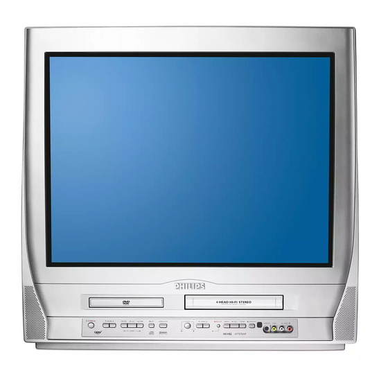
Color TV with Built-In VCR/DVD Player
Service
Service
Service
Service Manual
Contents
Chapter
Sec. 1: Adjustment Procedures
Schematic Diagrams and CBA's
Exploded Views
Mechanical and Electrical Parts Lists
Sec. 2: Standard Maintenance
Mechanism Alignment Procedures
Disassembly / Assembly of Mechanism
Deck Exploded Views
Deck Parts List
c Copyright 2006 Philips Consumer Electronics B.V. Eindhoven, The Netherlands.
All rights reserved. No part of this publication may be reproduced, stored in a retrieval
system or transmitted, in any form or by any means, electronic, mechanical, photocopying,
or otherwise without the prior permission of Philips.
Published by FU-KC 0611 Service AV Systems
Survey of versions:
/37
NTSC
Printed in The Netherlands
24MC4306/
CLASS 1 LASER PRODUCT
KLASSE 1 LASER PRODUKT
KLASS 1 LASER APPARAT
CLASSE 1 PRODUIT LASER
Subject to modification
37
EN 3139 785 31851
Advertisement
Chapters
Table of Contents

Related Manuals for Philips 24MC4306/37


Summary of Contents for Philips 24MC4306/37
- Page 1 Deck Exploded Views Deck Parts List c Copyright 2006 Philips Consumer Electronics B.V. Eindhoven, The Netherlands. All rights reserved. No part of this publication may be reproduced, stored in a retrieval system or transmitted, in any form or by any means, electronic, mechanical, photocopying, or otherwise without the prior permission of Philips.
-
Page 2: Table Of Contents
MAIN SECTION Color TV with Built-In VCR/DVD Player Sec. 1: Main Section I Adjustment Procedures I Schematic Diagrams and CBA’s I Exploded Views I Mechanical and Electrical Parts List TABLE OF CONTENTS LASER BEAM SAFETY PRECAUTIONS ........... . 1-1-1 IMPORTANT SAFETY PRECAUTIONS. -
Page 3: Laser Beam Safety Precautions
LASER BEAM SAFETY PRECAUTIONS This DVD player uses a pickup that emits a laser beam. Do not look directly at the laser beam coming from the pickup or allow it to strike against your skin. The laser beam is emitted from the location shown in the figure. When checking the laser diode, be sure to keep your eyes at least 30 cm away from the pickup lens when the diode is turned on. -
Page 4: Important Safety Precautions
IMPORTANT SAFETY PRECAUTIONS Prior to shipment from the factory, our products are strictly inspected for recognized product safety and electrical codes of the countries in which they are to be sold. However, in order to maintain such compliance, it is equally important to implement the following precautions when a set is being serviced. - Page 5 may be called “horizontal disable” or “hold regardless of the AC plug polarity. This chassis down.”) Read and apply the high voltage limits can be safety-serviced only with an isolation and, if the chassis is so equipped, the X- transformer inserted in the power line between radiation protection circuit specifications given the receiver and the AC power source, for both on instrument labels and in the Product Safety...
- Page 6 Precautions during Servicing A. Parts identified by the # symbol are critical for safety. Replace only with part number specified. B. In addition to safety, other parts and assemblies are specified for conformance with regulations applying to spurious radiation. These must also be replaced only with specified replacements.
- Page 7 Safety Check after Servicing Examine the area surrounding the repaired location for damage or deterioration. Observe that screws, parts and wires have been returned to original positions. Afterwards, perform the following tests and confirm the specified values in order to verify compliance with safety standards. 1.
-
Page 8: Standard Notes For Servicing
Due to lead-free technology some rules have to be respected by the workshop during a repair: Pin 1 • Use only lead-free solder alloy Philips SAC305 with order code 0622 149 00106. If lead-free solder- paste is required, please contact the manufacturer Instructions for Connectors of your solder-equipment. - Page 9 • Mix of lead-free solder alloy / parts with leaded How to Remove / Install Flat Pack-IC solder alloy / parts is possible but PHILIPS recommends strongly to avoid mixed solder alloy 1. Removal types (leaded and lead-free). With Hot-Air Flat Pack-IC Desoldering Machine: If one cannot avoid or does not know whether 1.
- Page 10 With Soldering Iron: With Iron Wire: 1. Using desoldering braid, remove the solder from 1. Using desoldering braid, remove the solder from all pins of the flat pack-IC. When you use solder all pins of the flat pack-IC. When you use solder flux which is applied to all pins of the flat pack-IC, flux which is applied to all pins of the flat pack-IC, you can remove it easily.
- Page 11 2. Installation Instructions for Handling Semi- 1. Using desoldering braid, remove the solder from conductors the foil of each pin of the flat pack-IC on the CBA Electrostatic breakdown of the semi-conductors may so you can install a replacement flat pack-IC more occur due to a potential difference caused by easily.
-
Page 12: Preparation For Servicing
PREPARATION FOR SERVICING How to Enter the Service Mode Adjustment Mode Caution 1: V. Shift/V.Size adjustment: See adjustment instructions page 1-7-5. 1. Optical sensors system are used for Tape Start and End Sensor on this equipment. Read this VOL o No need to use. -
Page 13: Operating Controls And Functions
OPERATING CONTROLS AND FUNCTIONS NOTE: Front and Rear Cabinet illustrations are different from the actual model since these pages are made extracts from the Owners Manual. 1-5-1 T2221IB... - Page 14 1-5-2 T2221IB...
- Page 15 1-5-3 T2221IB...
- Page 16 1-5-4 T2221IB...
-
Page 17: Cabinet Disassembly Instructions
CABINET DISASSEMBLY INSTRUCTIONS 1. Disassembly Flowchart Removal Step/ This flowchart indicates the disassembly steps for the Remove/*Unhook/ Loc. Part Fig. Unlock/Release/ cabinet parts, and the CBA in order to gain access to Note Unplug/Unclamp/ item(s) to be serviced. When reassembling, follow the Desolder steps in reverse order. - Page 18 Reference Notes in the Table 1) Disconnect Connector (CN301) on the DVD Main CBA Unit. CAUTION! 2) Short the three short lands of FPC cable with When removing the CRT, be sure to discharge the solder before removing the FFC cable (CN201) Anode Lead of the CRT with the CRT Ground Wire from it.
- Page 19 [2] Tray Chassis Unit Top Shield (S-5) (S-7) (S-5) (S-7) [4] DVD Mechanism (S-8) (S-8) (S-6) (S-6) (S-6) (S-8) [8] Deck Assembly [5] DVD Main CBA Unit [6] Sub CBA (S-11) (S-11) (S-11) [7] Function CBA [9] Main CBA (S-9) (S-10) Fig.
- Page 20 Anode Cap (S-4) CRT CBA (S-4) (S-4) [3] CRT (S-4) Fig. D3 DVD Mechanism Short the three short lands by soldering. (Either of two places.) View for A FPC Cable Fig. D4 1-6-4 T2221DC...
- Page 21 DVD MAIN CBA UNIT CN301 CN201 JUNCTION-B TO SPEAKER CN2A CN1A CL3801 ANODE CN3801 CN2801 CN2571 CL2501A SUB CBA CL2601 CN2503 CN2502 CN2401 FOCUS MAIN CBA CL2504A CL1403 CN1301 CN1602 CN1803 CL1401 SCREEN CN2501 CL2501B CRT CBA CL1402 CN1601 AC CORD CL1201 CN1802 TUNER...
-
Page 22: Electrical Adjustment Instructions
ELECTRICAL ADJUSTMENT INSTRUCTIONS General Note: “CBA” is abbreviation for How to enter the Service mode: “Circuit Board Assembly.” Service mode: Note: Electrical adjustments are required after 1. Use the service remote control unit. replacing circuit components and certain mechanical parts. It is important to perform 2. - Page 23 2. Setting for CONTRAST, COLOR, 3. H f 0 Adjustment TINT, V-TINT and SHARP Data Purpose: To get correct horizontal position and size of Values screen image. Symptom of Misadjustment: Horizontal position and General size of screen image may not be properly displayed. 1.
- Page 24 4. Cut-off Adjustment Test point Adj. Point Mode Input Purpose: To adjust the beam current of R, G, B, and VR2531 Monoscope screen voltage. Tape M. EQ. Spec. Symptom of Misadjustment: White color may be reddish, greenish or bluish. Pattern Generator 90+1%/-5% Test Point Adj.
- Page 25 7. White Balance Adjustment 8. Sub-Brightness Adjustment Purpose: To mix red, green and blue beams correctly Purpose: To get proper brightness. for pure white. Symptom of Misadjustment: If Sub-Brightness is Symptom of Misadjustment: White becomes bluish incorrect, proper brightness cannot be obtained by or reddish.
- Page 26 9. Focus Adjustment 11. V. Shift Adjustment Purpose: Set the optimum Focus. Purpose: To obtain correct vertical position of screen image. Symptom of Misadjustment: If Focus Adjustment is incorrect, blurred images are shown on the display. Symptom of Misadjustment: If V. position is incorrect, vertical position of image on the screen may Test Point Adj.
- Page 27 13. Head Switching Position The following 2 adjustments normally are not attempted in the field. They should be done only Adjustment when replacing the CRT then adjust as a preparation. Purpose: Determine the Head Switching Position during Playback. 14. Purity Adjustment Symptom of Misadjustment: May cause Head Purpose: To obtain pure color.
- Page 28 15. Convergence Adjustment 6. Fix the Deflection Yoke by carefully inserting the DY Wedges between CRT and Deflection Yoke. Purpose: To obtain proper convergence of red, green and blue beams. Symptom of Misadjustment: If Convergence Adjustment is incorrect, the edge of white letters may have color edges.
- Page 29 Adjustment Points and Test Points Main CBA VR1601 +B ADJ Sub CBA TP2504 VR2530 (GND) H. Pincushion TP2501 (+B Adjustment) VR2531 R2583 H.SIZE H ADJ. UPPER FOCUS VR LOWER SCREEN VR 1-7-8 T2221EA...
-
Page 30: How To Initialize The Tv/Dvd/Vcr
HOW TO INITIALIZE THE TV/DVD/VCR To put the program back at the factory-default, initialize the TV/DVD/VCR as the following procedure. < DVD Section > < TV/VCR Section > 1. Turn the power on and press [SELECT] button on 1. Use the service remote control unit. the remote control unit to put the TV/DVD/VCR 2. -
Page 31: Firmware Renewal Mode
FIRMWARE RENEWAL MODE 1. Turn the power on and press [SELECT] button on " ******* " differs depending on the models. the remote control unit to put the TV/DVD/VCR into DVD mode. Then remove the disc on the tray. F/W Version Up Mode Model No : ******* (It is possible to move to F/W version up mode VERSION : *.**... -
Page 32: Block Diagrams
BLOCK DIAGRAMS < TV/VCR Section > System Control / Servo Block Diagram T2221BLS 1-10-1... - Page 33 Video Block Diagram T2221BLV 1-10-2...
- Page 34 Audio Block Diagram T2221BLA 1-10-3...
- Page 35 Hi-Fi Audio Block Diagram T2221BLH 1-10-4...
- Page 36 TV Process Block Diagram T2221BLT 1-10-5...
- Page 37 CRT/H.V. Block Diagram T2221BLCRT 1-10-6...
- Page 38 Power Supply Block Diagram T2221BLP 1-10-7...
- Page 39 BLOCK DIAGRAMS < DVD Section > DVD System Control / Servo Block Diagram T2221BLSD 1-10-8...
- Page 40 Digital Signal Process Block Diagram T2221BLD 1-10-9...
-
Page 41: Schematic Diagrams / Cba's And Test Points
Distinction Area AREA D3 modified or altered without written permission from AREA B1 Line Number Philips Consumer Electronics Company. Philips (1 to 3 digits) assumes no liability, express or implied, arising out of 1-D3 any unauthorized modification of design. Servicer assumes all liability. - Page 42 Main 1/6 Schematic Diagram Parts Location Guide Ref No. Position Ref No. Position Ref No. Position Ref No. Position CAPACITORS DIODES RESISTORS RESISTORS C1203 D1217 R1220 R1263 C1207 D1224 R1221 R1267 C1208 D1229 R1222 R1270 C1210 D1230 R1224 R1273 C1212 D1231 R1225 R1274...
- Page 43 Main 1/6 & Sensor Schematic Diagram < TV/VCR Section > Voltage indications for PLAY, REC and DVD modes on the Schematic Diagrams are as shown below: PLAY mode “ “ = SMD REC mode (2.5) DVD mode < > The same voltage for Indicates that the voltage PLAY, REC &...
- Page 44 Main 2/6 Schematic Diagram < TV/VCR Section > Voltage indications for PLAY, REC and DVD modes on the Schematic Diagrams are as shown below: PLAY mode “ “ = SMD REC mode (2.5) DVD mode < > The same voltage for Indicates that the voltage PLAY, REC &...
- Page 45 Main 2/6 Schematic Diagram Parts Location Guide Ref No. Position Ref No. Position Ref No. Position CAPACITORS CAPACITORS RESISTORS C1410 C1466 R1411 C1411 C1468 R1412 C1413 C1469 R1413 C1414 C1870 R1415 C1415 C1871 R1416 C1417 C1872 R1417 C1418 C1873 R1418 C1419 CONNECTORS R1419...
- Page 46 Main 3/6 Schematic Diagram Parts Location Guide Ref No. Position Ref No. Position Ref No. Position CAPACITORS CAPACITORS RESISTORS C1004 C1342 R1050 C1008 C1350 R1053 C1030 DIODES R1301 C1034 D1032 R1303 C1035 D1302 R1305 C1036 D1303 R1308 C1037 D1304 R1310 C1040 D1305 R1313...
- Page 47 Main 3/6 Schematic Diagram < TV/VCR Section > Voltage indications for PLAY, REC and DVD modes on the Schematic Diagrams are as shown below: PLAY mode “ “ = SMD REC mode (2.5) DVD mode < > The same voltage for Indicates that the voltage PLAY, REC &...
- Page 48 Main 4/6 Schematic Diagram < TV/VCR Section > Voltage indications for PLAY, REC and DVD modes on the Schematic Diagrams are as shown below: PLAY mode “ “ = SMD REC mode (2.5) DVD mode < > The same voltage for Indicates that the voltage PLAY, REC &...
- Page 49 Main 4/6 Schematic Diagram Parts Location Guide Ref No. Position Ref No. Position Ref No. Position CAPACITORS CAPACITORS RESISTORS C1740 C1779 R1352 C1747 C1780 R1751 C1748 C1781 R1752 C1752 C1782 R1753 C1753 C1783 R1754 C1754 C1784 R1755 C1755 C1786 R1756 C1756 C1787 R1757...
- Page 50 Main 5/6 Schematic Diagram Parts Location Guide Ref No. Position Ref No. Position Ref No. Position CAPACITORS CONNECTORS RESISTORS C1117 CN1301 BB-2 R1802 C1118 CN1802 R1803 AA-2 C1801 CN1803 BB-4 R1808 AA-2 C1807 DIODES R1809 C1810 D1811 R1810 C1811 D1812 R1813 C1812 D1813...
- Page 51 Main 5/6 & Junction-A Schematic Diagram < TV/VCR Section > Voltage indications for PLAY, REC and DVD modes on the Schematic Diagrams are as shown below: PLAY mode “ “ = SMD REC mode (2.5) DVD mode < > The same voltage for Indicates that the voltage PLAY, REC &...
- Page 52 Main 6/6 Schematic Diagram < TV/VCR Section > VOLTAGE CHART (Power off mode) Ref. No. IC1601 25.7 24.7 CAUTION ! NOTE: Ref. No. Fixed voltage (or Auto voltage selectable) power supply circuit is used in this unit. The voltage for parts in hot circuit is measured using IC1682 If Main Fuse (F1601) is blown , check to see that all components in the power supply Ref.
- Page 53 Main 6/6 Schematic Diagram Parts Location Guide Ref No. Position Ref No. Position Ref No. Position Ref No. Position CAPACITORS DIODES TRANSISTORS RESISTORS C1206 GG-4 D1612 EE-4 Q1601 CC-2 R1635 FF-1 C1604 DD-3 D1613 EE-4 Q1602 DD-2 R1636 EE-4 C1605 CC-3 D1614 EE-3...
- Page 54 Main CBA Parts Location Guide Ref No. Position Ref No. Position Ref No. Position Ref No. Position Ref No. Position Ref No. Position Ref No. Position Ref No. Position Ref No. Position Ref No. Position CAPACITORS CAPACITORS CAPACITORS CAPACITORS DIODES TRANSISTORS RESISTORS RESISTORS...
- Page 55 Main CBA Top View < TV/VCR Section > Sensor CBA Top View CAUTION ! : For continued protection against risk of fire, NOTE: replace only with same type 4 A, 125V fuse. BHF300F01011A The voltage for parts in hot circuit is measured using Because a hot chassis ground is present in the power 4A 125V ATTENTION : Utiliser un fusible de rechange de même type de 4A, 125V.
- Page 56 Main CBA Bottom View < TV/VCR Section > CAUTION ! : For continued protection against risk of fire, NOTE: replace only with same type 4 A, 125V fuse. Because a hot chassis ground is present in the power The voltage for parts in hot circuit is measured using 4A 125V ATTENTION : Utiliser un fusible de rechange de même type de 4A, 125V.
- Page 57 CRT Schematic Diagram < TV/VCR Section > Voltage indications for PLAY, REC and DVD modes on the Schematic Diagrams are as shown below: PLAY mode “ “ = SMD REC mode (2.5) DVD mode < > The same voltage for Indicates that the voltage PLAY, REC &...
- Page 58 CRT CBA Top View < TV/VCR Section > CRT CBA Bottom View < TV/VCR Section > CRT CBA PARTS LOCATION GUIDE Ref No. Position Ref No. Position Ref No. Position CAPACITORS TRANSISTORS RESISTORS C2504 Q2502 R2516 C2505 Q2503 R2517 C2506 RESISTORS R2518 C2508...
- Page 59 Junction-A CBA Junction-A CBA Function CBA Top View < TV/VCR Section > Top View Bottom View < TV/VCR Section > < TV/VCR Section > BT1200F01022-D Junction-B CBA Junction-B CBA Top View Bottom View < TV/VCR Section > < TV/VCR Section > Function CBA Bottom View <...
- Page 60 Sub 1/2 Schematic Diagram < TV/VCR Section > Voltage indications for PLAY, REC and DVD modes on the Schematic Diagrams are as shown below: PLAY mode REC mode (2.5) DVD mode “ “ = SMD < > The same voltage for Indicates that the voltage PLAY, REC &...
- Page 61 Sub 1/2 Schematic Diagram Parts Location Guide Ref No. Position Ref No. Position Ref No. Position Ref No. Position CAPACITORS DIODES RESISTORS RESISTORS C2530 D2536 R2533 R2579 C2531 D2552 R2534 R2580 C2532 D2555 R2535 R2581 C2533 D2572 R2536 R2582 C2534 D2575 R2537 R2583...
- Page 62 Sub 2/2 Schematic Diagram Parts Location Guide Ref No. Position Ref No. Position Ref No. Position Ref No. Position CAPACITORS DIODES TRANSISTORS RESISTORS C2603 D2662 Q2701 R2672 C2604 D2703 RESISTORS R2675 C2605 R2201 R2676 C2616 IC2602 R2202 R2677 C2629 IC3603 R2203 R2678 C2630...
- Page 63 Sub 2/2 Schematic Diagram < TV/VCR Section > Voltage indications for PLAY, REC and DVD modes on the Schematic Diagrams are as shown below: PLAY mode “ “ = SMD REC mode (2.5) DVD mode < > The same voltage for Indicates that the voltage PLAY, REC &...
- Page 64 Sub CBA Parts Location Guide Ref No. Position Ref No. Position Ref No. Position Ref No. Position Ref No. Position Ref No. Position Ref No. Position Ref No. Position CAPACITORS CAPACITORS DIODES TRANSISTORS RESISTORS RESISTORS RESISTORS RESISTORS C2530 C2594 D2584 Q2202 R2532 R2564...
- Page 65 Sub CBA Top View < TV/VCR Section > TP2504 VR2530 PIN C. VR2531 H SIZE TP2501 R2583 (H f Adjustment) 1-11-25 BT1200F01022-A...
- Page 66 Sub CBA Bottom View < TV/VCR Section > WF17 WF18 WF19 TP2513 TP2512 PIN18 OF CN2503 DVD-Y DVD-C WF10 WF11 WF20 PIN2 Q2571 PIN 5 Collector CN2571 OF CN2 1-11-26 BT1200F01022-A...
- Page 67 DVD Main 1/3 Schematic Diagram < DVD Section > Voltage indications for PLAY and STOP modes on the Schematic Diagrams are as shown below: PLAY mode STOP mode “ “ = SMD (2.5) The same voltage for Indicates that the voltage both PLAY &...
- Page 68 DVD Main 2/3 Schematic Diagram < DVD Section > Voltage indications for PLAY and STOP modes on the Schematic Diagrams are as shown below: PLAY mode STOP mode “ “ = SMD (2.5) The same voltage for Indicates that the voltage both PLAY &...
- Page 69 DVD Main 3/3 Schematic Diagram < DVD Section > Voltage indications for PLAY and STOP modes on the Schematic Diagrams are as shown below: PLAY mode “ “ = SMD STOP mode (2.5) The same voltage for Indicates that the voltage both PLAY &...
-
Page 70: Waveforms
WAVEFORMS X7TWF 1-12-1... -
Page 71: Wiring Diagram < Tv/Vcr Section
WIRING DIAGRAM < TV/VCR Section > 1-13-1 T2221WIT... -
Page 72: Wiring Diagram < Dvd Section
WIRING DIAGRAM < DVD Section > T2221WID 1-13-2... -
Page 73: System Control Timing Charts
SYSTEM CONTROL TIMING CHARTS < TV/VCR Section > Mode SW: LD-SW LD-SW Position detection A/D Input voltage Limit Symbol (Calculated voltage) 3.76 V ~ 4.50 V (4.12 V) 4.51 V ~ 5.00 V (5.00 V) 0.00 V ~ 0.25 V (0.00 V) 1.06 V ~ 1.50 V (1.21 V) 0.66 V ~ 1.05 V (0.91 V) 1.99 V ~ 2.60 V (2.17 V) - Page 74 Chart 1 1) SP MODE 18 RF-SW The first rise of RF-SW after a rise in F-AD signal. F-AD ( Internal Signal ) "H" "H" "Z" C-DRIVE Stop Detection Acceleration Detection Slow Tracking Value PB CTL Reversal Limit Value 66 C-F/R ROLL COMPENSATION (DRUM SERVO)
- Page 75 Chart 2 2) LP/EP MODE 18 RF-SW The first rise of RF-SW after a rise in F-AD signal. F-AD ( Internal Signal ) "H" "H" "Z" C-DRIVE Stop Detection Acceleration Detection Slow Tracking Value PB CTL Reversal Limit Value 66 C-F/R ROLL COMPENSATION (DRUM SERVO)
- Page 76 Chart 3 EJECT ST-S/ END-S "OFF" CASS.LOAD LD-FWD 0.2S LD-REV SFT-SW STOP(B) POWER LD-FWD 0.4S 0.2S LD-REV 0.2S LD-FWD 0.5S LD-REV STOP(A) PLAY LD-FWD PLAY LD-FWD RS1(RS2) LD-REV 0.2S LD-FWD FS1(FS2) PLAY PLAY PAUSE (SLOW) LD-FWD STILL(SLOW) PLAY LD-REV 0.2S LD-FWD PLAY STOP...
- Page 77 Chart 4 STOP(A) STOP LD-REV 0.2S LD-FWD 0.2S STOP /EJECT 1.0S LD-FWD 0.5S LD-REV STOP(A) LD-REV 0.2S LD-FWD 0.2S STOP /EJECT LD-REV 1.0S LD-FWD 0.5S LD-REV STOP(A) LD-FWD PAUSE LD-FWD 2.5S Short REV LD-REV 0.2S LD-FWD REC PAUSE REC or PAUSE STOP /EJECT...
- Page 78 < DVD Section > Tray Close ~ Play / Play ~ Tray Open Tray Disc Disc Tray Play Close Rotation Stop Open 3.3V Tray IN (TL221) Sled Drive 1.65V (TP303) Disc Drive 1.65V (TP301) 1.65V Focus Drive (TP304) Tracking Drive 1.65V (TP302) 1-14-6...
-
Page 79: Ic Pin Function Descriptions
IC PIN FUNCTION DESCRIPTIONS IC1201 (TV/VCR Micro Controller IC) Signal Function Name “H” ≥ 4.5 V, “L” ≤ 1.0 V System Reset Signal (Reset IN RESET = “L”) Signal Function Name IN XC-IN Sub Clock (32kHz) IN LD-SW Loading Switch Input 36 OUT XC-OUT Sub Clock (32kHz) OUT DVD-LED... - Page 80 Signal Function Name 70 OUT YCA-SCL YCA Serial Clock 71 OUT SCL Serial Clock Serial Data Not Used IN C-SYNC Composite Sync Input Not Used Capstan Motor Control 76 OUT C-CONT Signal 77 OUT D-CONT Drum Motor Control Signal P-SAFETY Power Supply Failure Detection 3 Not Used...
-
Page 81: Lead Identifications
LEAD IDENTIFICATIONS MID-32A22F 2SK3561 PT204-6B-12 2SC2785(F) 2SA1175(F) 2SA950-(O,Y)(TE2 F T) 2SC3400 2SA1015-GR(TE2 F T) BA1F4M-T 2SC1815-(GR,Y)(TE2 F T) KRA103M-AT/P 2SC2120-(O,Y)(TE2 F T) KRC103M-AT/P 2SC1627-Y(TE2.F.T) KTA1267-GR-AT/P 2SC3331(T,U) KTC3199-GR-AT/P 2SC3708(S,T) KTC3199-Y-AT/P 2SD400(E,F) KTC3205-Y-AT/P KTA1271-Y-AT/P KTA-1266-GR-AT/P S D G KTC3198-GR-AT/P E C B E C B LA78041-E AN17812A... -
Page 82: Electrical Parts List
ELECTRICAL PARTS LIST PRODUCT SAFETY NOTE: Products marked with a # have special characteristics important to safety. Before replacing any of these components, read carefully the product safety notice in this service manual. Don't degrade the safety of the product through improper servicing. NOTES: Parts that are not assigned part numbers (---------) are not available. - Page 83 ELECTRICAL PARTS LIST Pos.No. # 12 NC Description T1601 9965 000 34700 TRANS POWER 6725-S01 HEAD SHIELD T1200UA TB13 BUSH LED(F) H3700UD TB17 X7 MAIN HEAT SINK PLG ASSEMBLY T2200UA SCREW B-TIGHT D3X8 BIND HEAD+ TP1202 PCB JUMPER D0.6-P16.0 TP1301 PCB JUMPER D0.6-P9.0 TP1302 PCB JUMPER D0.6-P8.0...
- Page 84 ELECTRICAL PARTS LIST Pos.No. # 12 NC Description C1213 CHIP CERAMIC CAP .(1608) CH J 22PF/50V C1214 ELECTROLYTIC CAP . 47UF/6.3V M H7 C1214 ALUMINUM ELECTROLYTIC CAP 47UF/6.3V H7 C1217 CHIP CERAMIC CAP .(1608) CH D 10PF/50V C1218 CHIP CERAMIC CAP . CH J 15PF/50V C1222 CHIP CERAMIC CAP .
- Page 85 ELECTRICAL PARTS LIST Pos.No. # 12 NC Description C1414 CHIP RES.(1608) 1/10W 0 OHM C1415 ELECTROLYTIC CAP . 100UF/6.3V H7 C1415 ALUMINUM ELECTROLYTIC CAP 100UF/6.3V H7 C1417 CHIP CERAMIC CAP . CH J 220PF/50V C1418 CHIP CERAMIC CAP . F Z 1UF/10V C1419 CHIP CERAMIC CAP .
- Page 86 ELECTRICAL PARTS LIST Pos.No. # 12 NC Description C1613 FILM CAP .(P) 0.0018UF/50V J C1613 POLYESTER FILM CAP . (PB FREE) 0.0018UF/100V J C1614 FILM CAP .(P) 0.1UF/50V J C1614 FILM CAP .(P) 0.1UF/50V J C1614 9965 000 34715 POLYESTER FILM CAP . (PB FREE) 0.1UF/100V J C1615 9965 000 22652 CERAMIC CAP .
- Page 87 ELECTRICAL PARTS LIST Pos.No. # 12 NC Description C1760 CHIP CERAMIC CAP .(1608) B K 4700PF/50V C1762 CHIP CERAMIC CAP .(1608) B K 0.01UF/50V C1763 CHIP CERAMIC CAP .(1608) B K 0.01UF/50V C1764 ELECTROLYTIC CAP . 100UF/10V M H7 C1764 ALUMINUM ELECTROLYTIC CAP 100UF/10V H7 C1766 ELECTROLYTIC CAP .
- Page 88 ELECTRICAL PARTS LIST Pos.No. # 12 NC Description C1821 ELECTROLYTIC CAP . 470UF/16V M C1821 ELECTROLYTIC CAP . 470UF/16V M C1822 ELECTROLYTIC CAP . 470UF/16V M C1822 ELECTROLYTIC CAP . 470UF/16V M C1822 ELECTROLYTIC CAP . 470UF/16V M C1870 ELECTROLYTIC CAP . 47UF/6.3V M H7 C1870 ALUMINUM ELECTROLYTIC CAP 47UF/6.3V H7 C1871...
- Page 89 ELECTRICAL PARTS LIST Pos.No. # 12 NC Description D1606 9965 000 28909 DIODE 1N5406 D1606 9965 000 28910 DIODE ERC04-06L3 D1607 9965 000 18164 ZENER DIODE MTZJT-7724C D1607 4822 130 34398 ZENER DIODE DZ-24BSCT265 D1609 4822 130 32778 SWITCHING DIODE 1SS133(T-77) D1610 4822 130 83166 ZENER DIODE MTZJT-776.2B D1610...
- Page 90 ELECTRICAL PARTS LIST Pos.No. # 12 NC Description D1684 4822 130 30621 SWITCHING DIODE 1N4148 D1687 4822 130 32778 SWITCHING DIODE 1SS133(T-77) D1687 4822 130 30621 SWITCHING DIODE 1N4148 D1688 4822 130 32778 SWITCHING DIODE 1SS133(T-77) D1688 4822 130 30621 SWITCHING DIODE 1N4148 D1691 ELECTROLYTIC CAP .
- Page 91 ELECTRICAL PARTS LIST Pos.No. # 12 NC Description Q1604 9965 000 29485 TRANSISTOR KTC3199-GR-AT/P Q1604 9965 000 29487 TRANSISTOR 2SC1815-GR(TE2 F T) Q1604 9965 000 34678 TRANSISTOR KTC3198-GR-AT/P Q1605 9965 000 05643 TRANSISTOR 2SC2785(F) Q1605 9965 000 29485 TRANSISTOR KTC3199-GR-AT/P Q1605 9965 000 29487 TRANSISTOR 2SC1815-GR(TE2 F T) Q1605...
- Page 92 ELECTRICAL PARTS LIST Pos.No. # 12 NC Description R1200 CHIP RES. 1/10W J 1K OHM R1201 CHIP RES. 1/16W G 4.7K OHM R1202 CHIP RES. 1/16W G 22K OHM R1203 CHIP RES. 1/16W G 470 OHM R1204 CHIP RES. 1/16W G 1.5K OHM R1205 CHIP RES.
- Page 93 ELECTRICAL PARTS LIST Pos.No. # 12 NC Description R1285 CHIP RES. 1/10W J 3.3K OHM R1286 CHIP RES. 1/10W J 3.3K OHM R1287 CHIP RES.(1608) 1/10W 0 OHM R1289 CHIP RES.(1608) 1/10W 0 OHM R1290 CHIP RES.(1608) 1/10W 0 OHM R1298 CHIP RES.
- Page 94 ELECTRICAL PARTS LIST Pos.No. # 12 NC Description R1617 CARBON RES. 1/4W J 180 OHM R1618 PCB JUMPER D0.6-P5. R1619 9965 000 34684 METAL OXIDE FILM RES. 1W J 2.7K OHM R1619 9965 000 34685 METAL OXIDE FILM RES. 1W J 2.7K OHM R1620 9965 000 34684 METAL OXIDE FILM RES.
- Page 95 ELECTRICAL PARTS LIST Pos.No. # 12 NC Description R1774 CHIP RES. 1/10W J 22K OHM R1780 CHIP RES. 1/10W J 6.8K OHM R1781 CHIP RES. 1/10W J 8.2K OHM R1801 9965 000 22682 CARBON RES. 1/4W J 180 OHM R1802 9965 000 22682 CARBON RES.
- Page 96 ELECTRICAL PARTS LIST Pos.No. # 12 NC Description CL2601 LEAD WIRE 5P 370MM X7 H/V HEAT SINK PLH ASSEMBLY T2200UA SCREW B-TIGHT D3X8 BIND HEAD+ JK2701 9965 000 34732 JACK RCA PCB L MSP-241V-05 NI LFW/O T2571 9965 000 34733 TRANS FBT JF0501-3301-G T2571 9965 000 35229 FLYBACK TRANS BW03072 T2572A...
- Page 97 ELECTRICAL PARTS LIST Pos.No. # 12 NC Description C2574 9965 000 22656 ELECTROLYTIC CAP . 4.7UF/250V M C2574 9965 000 34721 ALUMINUM ELECTROLYTIC CAP 4.7UF/250V M C2577 FILM CAP .(P) 0.018UF/50V J C2577 FILM CAP .(P) 0.018UF/50V J C2577 9965 000 34671 POLYESTER FILM CAP . (PB FREE) 0.018UF/100V J C2578 ELECTROLYTIC CAP .
- Page 98 ELECTRICAL PARTS LIST Pos.No. # 12 NC Description D2575 9965 000 09283 ZENER DIODE DZ-10BSBT265 D2583 4822 130 32778 SWITCHING DIODE 1SS133(T-77) D2583 4822 130 30621 SWITCHING DIODE 1N4148 D2584 4822 130 32778 SWITCHING DIODE 1SS133(T-77) D2584 4822 130 30621 SWITCHING DIODE 1N4148 D2585 4822 130 82703 ZENER DIODE MTZJT-775.1B D2585...
- Page 99 ELECTRICAL PARTS LIST Pos.No. # 12 NC Description Q2530 9965 000 34729 TRANSISTOR KTD2059-Y/P Q2531 9965 000 05644 TRANSISTOR 2SA1175(F) Q2531 9965 000 29491 TRANSISTOR KTA1267-GR-AT/P Q2531 9965 000 29494 TRANSISTOR 2SA1015-GR(TE2 F T) Q2531 9965 000 29493 TRANSISTOR KTA-1266-GR-AT/P Q2532 9965 000 05643 TRANSISTOR 2SC2785(F) Q2532...
- Page 100 ELECTRICAL PARTS LIST Pos.No. # 12 NC Description R2535 CHIP RES. 1/10W J 18K OHM R2536 CHIP RES. 1/10W J 100K OHM R2537 CARBON RES. 1/4W J 2.7K OHM R2538 CHIP RES. 1/10W J 1.2K OHM R2539 9965 000 09956 CHIP RES. 1/10W J 100K OHM R2540 CHIP RES.
- Page 101 ELECTRICAL PARTS LIST Pos.No. # 12 NC Description R2657 CHIP RES. 1/10W J 22K OHM R2658 CHIP RES. 1/10W J 1K OHM R2659 CHIP RES. 1/10W J 820 OHM R2660 CHIP RES. 1/10W J 820 OHM R2671 CHIP RES. 1/10W F 5.6K OHM R2671 CHIP RES.
- Page 102 ELECTRICAL PARTS LIST Pos.No. # 12 NC Description R2521 CARBON RES. 1/4W J 1.5K OHM R2522 CARBON RES. 1/4W J 1.5K OHM R2523 CARBON RES. 1/4W J 1.5K OHM R2524 CARBON RES. 1/4W J 1.5K OHM FUNCTION CBA (MPS-C) CONNECTORS CN2401 BOARD CONNECTOR 07P(PB FREE) 127301107K2 CN2801...
-
Page 103: Exploded Views
EXPLODED VIEWS Cabinet SHINWHA TAPE SGT-730 (BLACK) Details for L551 V501-2 and surrounding parts SHINWHA TAPE SGT-730 V501-1 (WHITE) L551 Scotch L3-1 Tape #880 CRT CBA CLN551 CLN551 CLN551 TB18 DVD Mechanical Parts L3-2 TL1-1 TL1-1 Scotch TL1-1 Tape #880 DG601 V501 TL1-2... - Page 104 Packing X2-1 X2-2 X2-3 Packing Tape Tape 1-18-2 T2221PEX...
-
Page 105: Mechanical Parts List
MECHANICAL PARTS LIST PRODUCT SAFETY NOTE: Products marked with a # have special characteristics important to safety. Before replacing any of these components, read carefully the product safety notice in this service manual. Don't degrade the safety of the product through improper servicing. MECHANICAL PARTS LIST Pos.No. - Page 106 MECHANICAL PARTS LIST Pos.No. 12 NC Description X2-1 OWNERS MANUAL T1201UB X2-2 OWNERS MANUAL(SP) T1201UB X2-3 OWNERS MANUAL(FR) T1201UB 9965 000 34654 REMOTE CONTROL NF401UD 151/ECNX701/NF401UD DRY BATTERY R03/2S CARD REGISTRATION (EN) TD957UH QUICK SETUP GUIDE T1201UB QUICK SETUP GUIDE(SP) T1201UB QUICK SETUP GUIDE(FR) T1201UB CRT TYPE A L551...
- Page 107 DECK MECHANISM SECTION Color TV with Built-In VCR/DVD Player Sec. 2: Deck Mechanism Section I Standard Maintenance I Mechanism Alignment Procedures I Disassembly / Assembly of Mechanism I Deck Exploded Views I Deck Parts List TABLE OF CONTENTS STANDARD MAINTENANCE............. . 2-1-1 SERVICE FIXTURE AND TOOLS .
-
Page 108: Standard Maintenance
STANDARD MAINTENANCE Service Schedule of Components This maintenance chart shows you the standard of replacement and cleaning time for each part. Because those may replace depending on environment and purpose for use, use the chart for reference. Deck Periodic Service Schedule Ref.No. - Page 109 Cleaning Cleaning of ACE Head Clean the head with a cotton swab. Cleaning of Video Head Procedure Clean the head with a head cleaning stick or chamois 1. Remove the top cabinet. cloth. 2. Dip the cotton swab in 90% ethyl alcohol and clean Procedure the ACE Head.
-
Page 110: Service Fixture And Tools
SERVICE FIXTURE AND TOOLS Back Tension Meter Flat Screw Driver VFMS0001H6 (Made in USA) (Purchase Locally) Alignment Tape Post Adjustment Screwdriver Metric Thickness Gauges Lock Screw Driver (Purchase Locally) (Purchase Locally) Head Cleaning Stick 2-2-1 MK14FIX_PC... -
Page 111: Mechanical Alignment Procedures
MECHANICAL ALIGNMENT PROCEDURES Explanation of alignment for the tape to correctly run B. Method to place the Cassette Holder in the tape- starts on the next page. Refer to the information loaded position without a cassette tape below on this page if a tape gets stuck, for example, in 1. - Page 112 1. Tape Interchangeability Alignment Note: To do these alignment procedures, make sure that the Tracking Control Circuit is set to the preset position every time a tape is loaded or unloaded. (Refer to page 2-3-4, procedure 1-C, step 2.) Equipment required: Dual Trace Oscilloscope VHS Alignment Tape (VFMS0001H6) Guide Roller Adj.
- Page 113 1-A. Preliminary/Final Checking and 4. If creasing or snaking is apparent, adjust the Tilt Adj. Screw of the ACE Head. (Fig. M6) Alignment of Tape Path Purpose: To make sure that the tape path is well stabilized. Azimuth Adj. Screw Symptom of Misalignment: If the tape path is unstable, the tape will be damaged.
- Page 114 5. To shift the CTL waveform, press [CHANNEL K] 5. When Guide Rollers [2] and [3] (Refer to Fig. M3) or [CHANNEL L] buttons on the unit. Then make are aligned properly, there is no envelope drop sure that the maximum output position of PB FM either at the beginning or end of track as shown in ±...
- Page 115 1-D. Azimuth Alignment of Audio/Control/ Erase Head Correct Incorrect Purpose: To correct the Azimuth alignment so that the Audio/Control/Erase Head meets tape tracks Post [5] properly. Tape Symptom of Misalignment: If the position of the Audio/Control/Erase Head is not properly aligned, the Audio S/N Ratio or Frequency Response will be poor.
-
Page 116: Disassembly/Assembly Procedures Of Deck Mechanism
DISASSEMBLY/ASSEMBLY PROCEDURES OF DECK MECHANISM Before following the procedures described below, be sure to remove the deck assembly from the cabinet. (Refer to CABINET DISASSEMBLY INSTRUCTIONS of Main Section.) All the following procedures, including those for adjustment and replacement of parts, should be done in Eject mode;... - Page 117 Removal Installation Step Starting Remove/*Unhook/ /Loc. Part Adjustment Fig. No. Unlock/Release/ Condition Unplug/Desolder (+)Refer to Alignment [32] [25] Loading Arm (SP) Assembly B DM2, DM14 Sec.Page 2-5-1 (+)Refer to Alignment [33] [32] Loading Arm (TU) Assembly B DM2, DM14 Sec.Page 2-5-1 [34] [2], [25] M Brake (TU) Assembly DM1, DM15...
- Page 118 Top View [41] [42] [43] [46] [14] [13] [11] [15] [36] [10] [12] [35] [34] [40] [29] [30] [16] [39] [38] Fig. DM1 Bottom View [20] [33] [32] [24] [26] [27] [25] [23] [28] [22] [21] [31] Fig. DM2 2-4-3 N2466FTDA...
- Page 119 (S-1) (S-1) (L-1) (L-3) (L-2) (S-1A) (P-1) Installation of [3] and [6] First, insert [6] diagonally in [3] as shown below. Then, install [6] in [3] while pushing (L-1) in a direction of arrow. After installing [6] in [3], confirm that pin A of [3] enters hole A of [6] properly.
- Page 120 [11] (S-4A) (L-4) [46] (P-3) [13] [47] Removal of [11] [12] (L-14) 1) Remove screw (S-4A). 2) Unhook spring (P-2). [10] Release (L-4) while (P-2) holding [12] with a finger. Loosen a finger holding [12] and remove [11]. (S-2) Pin of [12] Pin of [10] Groove of [28] When reassembling [10] and...
- Page 121 Installation of [13] and [12] (S-5) [14] (S-6) [16] [13] [15] Hook spring (P-3) up to [12] and [13], then install them to (P-3) the specified position so that [12] will be floated slightly while holding [12] and [13]. (Refer to Fig. A.) [12] Fig.
- Page 122 (S-8) [22] (C-2) (C-1) [23] (L-6) [21] (P-5) [20] Cap Belt (P-5) [28] Installation position of Cap Belt [21] Cap Belt When installing [23], install the spring (P-5) to [28] as shown in the left figure, and then install [23] while Pin on pressing the spring (P-5) in bottom...
- Page 123 (P-6) [25] (C-4) [31] Refer to the Alignment Section, Page 2-5-1. (S-9) [29] [33] [30] (L-11) (L-10) [32] (L-8) (C-3) [27] [28] [24] [26] (L-9) Fig. DM14 Fig. DM13-1 [36] Break belt (P-7) Installation of [25] [34] Position of Mode Lever when installed [40] Pin of [35] Pin of [31]...
- Page 124 [42] [41] [43] (L-13) Fig. DM16 (P-9) [44] [45] Slide Fig. DM17 2-4-9 N2466FTDA...
-
Page 125: Alignment Procedures Of Mechanism
ALIGNMENT PROCEDURES OF MECHANISM The following procedures describe how to align the Alignment 1 individual gears and levers that make up the tape Loading Arm (SP) and (TU) Assembly loading/unloading mechanism. Since information about the state of the mechanism is provided to the Install Loading Arm (SP) and (TU) Assembly so System Control Circuit only through the Mode Switch, that their triangle marks point to each other as... -
Page 126: Deck Exploded Views
DECK EXPLODED VIEWS Deck Mechanism View 1 Mark Description Floil G-684G or Multemp MH-D (Blue grease) SLIDUS OIL #150 B494 L1467 L1191 B553 B411 B567 L1053 B410 L1051 Chassis Assembly Top View (Lubricating Point) B501 B560 L1450 L1450 B426 L1466 B121 B126 B492... - Page 127 Deck Mechanism View 2 Mark Description Floil G-684G or Multemp MH-D (Blue grease) B587 B521 B487 SLIDUS OIL #150 B416 B591 SANKOUL FG84M (Yellow grease) B520 B590 B522 L1406 B148 B499 B508 B573 B592 B574 B558 B564 B557 B414 B565 B525 L1151 B417...
- Page 128 Deck Mechanism View 3 Mark Description Floil G-684G or Multemp MH-D (Blue grease) L1321 SLIDUS OIL #150 B347 L1321 B355 B354 B483 L1341 B425 B482 B562 B300 B563 B313 L1474 B529 B360 B359 B361 B555 B561 B303 Some Ref. Numbers are not in sequence. B514 2-6-3 N2466FTDEX...
-
Page 129: Deck Parts List
DECK PARTS LIST DECK PARTS LIST Pos.No. 12 NC Description CYLINDER ASSEMBLY MK14 NTSC 6HD CYLINDER ASSEMBLY MK14 NTSC 6HD LOADING MOTOR ASSEMBLY MK14 PULLEY ASSEMBLY MK12 MOVING GUIDE S P .P MK12.5 MOVING GUIDE T P .P MK12.5 LOADING ARM(TU) ASSEMBLY MK12 LOADING ARM(SP) ASSEMBLY MK12 AC HEAD ASSEMBLY TVCR MK12.5 TAPE GUIDE ARM ASSEMBLY MK12.5... - Page 130 DECK PARTS LIST Pos.No. 12 NC Description B555 RACK ASSEMBLY MK14 B557 MOTOR PULLEY U5 B558 LOADING MOTOR RF-500TB-12560 B559 CLUTCH ASSEMBLY MK12 B559 CLUTCH ASSEMBLY(64) MK12 B560 KICK SPRING MK10 B561 F DOOR SPRING MK10 B562 C DRIVE LEVER(SP) MK12 B563 SLIDER SHAFT MK12 B564...
- Page 131 REVISION LIST Version 1.0 * Original Release Version 1.1 * Correction of pages 1-7-1 and 1-7-2 (high-lighted in Red)