Table of Contents
Advertisement
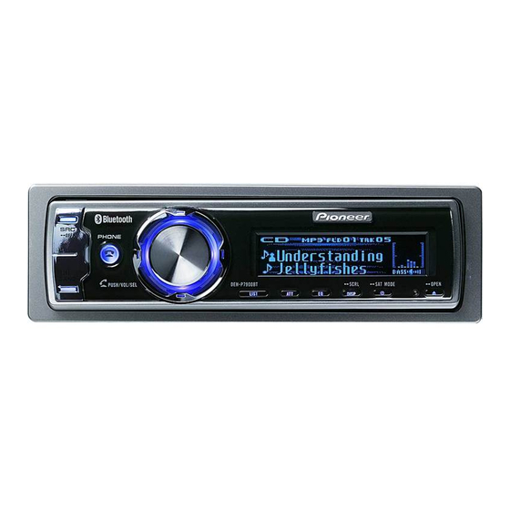
CD RECEIVER
DEH-P790BT
DEH-P7900BT
DEH-P8950BT
This service manual should be used together with the following manual(s):
Model No.
Order No.
CX-3195
CRT3815
For details, refer to "Important Check Points for Good Servicing".
PIONEER CORPORATION
PIONEER ELECTRONICS (USA) INC. P.O. Box 1760, Long Beach, CA 90801-1760, U.S.A.
PIONEER EUROPE NV Haven 1087, Keetberglaan 1, 9120 Melsele, Belgium
PIONEER ELECTRONICS ASIACENTRE PTE. LTD. 253 Alexandra Road, #04-01, Singapore 159936
PIONEER CORPORATION 2007
Mech.Module
S10.5COMP2
CD Mech. Module : Circuit Descriptions, Mech. Descriptions, Disassembly
4-1, Meguro 1-chome, Meguro-ku, Tokyo 153-8654, Japan
DEH-P790BT/XN/UC
/XN/UC
/XN/ES
Remarks
ORDER NO.
CRT3903
/XN/UC
K-ZZA. MAR. 2007 Printed in Japan
Advertisement
Table of Contents

Related Manuals for Pioneer DEH-P790BT


Summary of Contents for Pioneer DEH-P790BT
- Page 1 PIONEER CORPORATION 4-1, Meguro 1-chome, Meguro-ku, Tokyo 153-8654, Japan PIONEER ELECTRONICS (USA) INC. P.O. Box 1760, Long Beach, CA 90801-1760, U.S.A. PIONEER EUROPE NV Haven 1087, Keetberglaan 1, 9120 Melsele, Belgium PIONEER ELECTRONICS ASIACENTRE PTE. LTD. 253 Alexandra Road, #04-01, Singapore 159936 PIONEER CORPORATION 2007 K-ZZA.
-
Page 2: Safety Information
5. Be careful in handling ICs. Some ICs such as MOS type are so fragile that they can be damaged by electrostatic induction. 6. When diagnosing a product, take care of its heated portion. Holder (CND3133) Bluetooth Unit DEH-P790BT/XN/UC... - Page 3 To protect products from damages or failures during transit, the shipping mode should be set or the shipping screws should be installed before shipment. Please be sure to follow this method especially if it is specified in this manual. DEH-P790BT/XN/UC...
-
Page 4: Table Of Contents
CONTENTS SAFETY INFORMATION............................. 2 1. SPECIFICATIONS ............................5 2. EXPLODED VIEWS AND PARTS LIST......................8 2.1 PACKING(DEH-P790BT/XN/UC)....................... 8 2.2 PACKING(DEH-P7900/BT/XN/UC, DEH-P8950BT/XN/ES) ..............10 2.3 EXTERIOR(1) ............................12 2.4 EXTERIOR(2) ............................14 2.5 CD MECHANISM MODULE........................16 3. BLOCK DIAGRAM AND SCHEMATIC DIAGRAM ..................18 3.1 BLOCK DIAGRAM ........................... -
Page 5: Specifications
1. SPECIFICATIONS DEH-P790BT/XN/UC... - Page 6 DEH-P790BT/XN/UC...
- Page 7 DEH-P790BT/XN/UC...
-
Page 8: Exploded Views And Parts List
Screw adjacent to mark on the product are used for disassembly. For the applying amount of lubricants or glue, follow the instructions in this manual. (In the case of no amount instructions,apply as you think it appropriate.) 2.1 PACKING(DEH-P790BT/XN/UC) DEH-P790BT/XN/UC packing DEH-P790BT/XN/UC... - Page 9 PACKING(DEH-P790BT/XN/UC) SECTION PARTS LIST Mark No. Description Part No. Cord Assy CDE8284 Cord Assy CDP1009 Accessory Assy CEA7537 Cord Clamper Assy CEA4636 Clamper CNV8262 Polyethylene Bag E36-615 Screw Assy CEA5322 Screw CBA1650 Polyethylene Bag CEG-127 Screw CRZ50P090FTC Screw JPZ20P060FTB Screw...
-
Page 10: Packing(Deh-P7900/Bt/Xn/Uc, Deh-P8950Bt/Xn/Es)
2.2 PACKING(DEH-P7900/BT/XN/UC, DEH-P8950BT/XN/ES) DEH-P7900 & 8950 packing 10 10 DEH-P790BT/XN/UC... - Page 11 Not used 27-8 Caution Card CRP1358 Not used Polyethylene Bag CEG1173 CEG-162 Owner's Manual,Installation Manual Part No. Language CRD4205 English, French CRD4206 English, Spanish, Portuguese(B) CRD4207 Arabic, Traditional Chinese CRD4210 English, French CRD4211 English, Spanish, Portuguese(B), Arabic, Traditional Chinese DEH-P790BT/XN/UC...
-
Page 12: Exterior(1)
2.3 EXTERIOR(1) DEH-P790BT/XN/UC 1/2 DEH-P790BT/XN/UC... - Page 13 Resistor RS1/2PMF102J Lighting Conductor CNV9509 Connector(CN1961) CKS5545 Cord Assy See Contrast table(2) Connector(CN1801) CKS5662 (2) CONTRAST TABLE DEH-P790BT/XN/UC, DEH-P7900BT/XN/UC and DEH-P8950BT/XN/ES are constructed the same except for the following: Mark Description DEH-P790BT/XN/UC DEH-P7900BT/XN/UC DEH-P8950BT/XN/ES Panel CNS8914 CNS8915 CNS8915 Detach Grille Assy...
-
Page 14: Exterior(2)
2.4 EXTERIOR(2) 45 53 24 20 : GEM1024 : GEM1069 DEH-P790BT/XN/UC... - Page 15 Screw(M2 x 2) CBA1871 IC(IC911) NJM2388F84 Transistor(Q453,Q751,Q901) 2SD2396 Screw(M2 x 2) CBA1935 Spring CBH2530 (2) CONTRAST TABLE DEH-P790BT/XN/UC, DEH-P7900BT/XN/UC and DEH-P8950BT/XN/ES are constructed the same except for the following: Mark Description DEH-P790BT/XN/UC DEH-P7900BT/XN/UC DEH-P8950BT/XN/ES Tuner Amp Unit CWN2343 CWN2343 CWN2344...
-
Page 16: Cd Mechanism Module
2.5 CD MECHANISM MODULE DEH-P790BT/XN/UC... - Page 17 Bracket CND2583 CND2584 Lever CND2585 CND2586 Bracket CND2587 CND2588 Lever CND2589 Holder CNV7201 Gear CNV7207 Gear CNV7208 Gear CNV7209 Gear CNV7210 Gear CNV7211 Gear CNV7212 Rack CNV7214 CNV7216 Roller CNV7218 Gear CNV7219 Guide CNV7361 Gear CNV7595 Guide CNV7799 CNV7805 DEH-P790BT/XN/UC...
-
Page 18: Block Diagram And Schematic Diagram
3.3V 2.5V 2.5V 3.3V CONT2 Q261 TUN3V IC263 TC7SET08FU CN522 CN521 ROMCK ROMDATA PEE2 MICIN A:DEH-P7900BT/UC TELOUT EVOLSW3 EMUTE HFAV B:DEH-P790BT/UC BTRST SACLK MUTE SAOUT C:DEH-P8950BT/ES Q541 MUTE BOOTE SYSPW BTRST BTMUTE BTMUTE BTTEST BTTEST DACCS DACCS MEMDI DACDT CN76... - Page 19 ILMPW PVSENS Q561 ROT0 FWPWR ROT0 SWVDD ROT1 ROT1 Q562 Q841 SWVDD Q564 Q563 Q565 RESET SWVDD CN1801 IC651 RESET S-80835CNMC-B8U Q651 RESET DSENS DSENS DPDT DPDT KYDT KYDT OEL+B Q851 OEL+B Q852 IC851 OELB NJM2360M OELPW DC-DC CONVERTER DEH-P790BT/XN/UC...
- Page 20 XOUT IC1931 CN1961 OPT IN GP1UX31RK DPDT DPDT KYDT KYDT CLK0 ADATA DSENS OELD DSEL DSEL SWVDD BYTE OEL+B OEL+B AVCC1 OEL UNIT OEL+B DATA S1801 IC1921 AVCC2 Q1961 RESET :PD8171A RESET ADDRESS :PD8172A Q1962 CVCC A:DEH-P7900BT/UC B:DEH-P790BT/UC C:DEH-P8950BT/ES DEH-P790BT/XN/UC...
- Page 21 SCIF1_CTS BTCTS SCIF1_RTS BTTX SCIF1_RXD BTRX SCIF1_TXD SCIF0_RXD SCIF0_TXD BOOTE BOOT_E OCTS SCIF0_CTS ORTS SCIF0_RTS CLOCK SELECT IC22 IC21 TC7PAU04FU TC74VHC02FTS1 BT3V BT3V SIOF_MCLK HFAV HFMCK SCO_CLK_OUT X21 11.2896MHz IC23 TC7PAU04FU BT3V X22 12.288MHz HFAV HFAV SIOF_SS1 FSCHG PTB1 DEH-P790BT/XN/UC...
-
Page 22: Overall Connection Diagram(Guide Page)
Large size SCH diagram (ipod video:0dB play) Guide page +1.3dBs +2.2dBs +3.01dBs Detailed page CN701 (0dB play) +0.6dBs FM(30%):-24dBs AM(30%):-24dBs (0dB play) +2.2dBs CN1801 FLAP MOTOR XXA7400 : The power supply is shown with the marked box. SW UNIT DEH-P790BT/XN/UC... - Page 23 The > mark found on some component parts indicates the importance of the safety factor of the part. No differentiation is made between chip capacitors and 0.022 R022 Therefore, when replacing, be sure to use parts of identical designation. discrete capacitors. DEH-P790BT/XN/UC...
- Page 24 DEH-P790BT/XN/UC...
- Page 25 DEH-P790BT/XN/UC...
- Page 26 DEH-P790BT/XN/UC...
- Page 27 DEH-P790BT/XN/UC...
-
Page 28: Keyboard Unit
3.3 KEYBOARD UNIT CN801 DEH-P790BT/XN/UC... - Page 29 KEYBOARD UNIT OEL UNIT MXS8231 DEH-P790BT/XN/UC...
-
Page 30: Cd Mechanism Module(Guide Page)
3.4 CD MECHANISM MODULE(GUIDE PAGE) PICKUP UNIT(P10.5)(SERVICE) SWITCHES: CD CORE UNIT(S10.5COMP2) S901:HOME SWITCH..ON-OFF S903:DSCSNS SWITCH..ON-OFF S904:12EJ SWITCH.....ON-OFF S905:8EJ SWITCH....ON-OFF The underlined indicates the switch position. M1 CXC7134 SPINDLE MOTOR M2 CXC4026 LOADING/CARRIAGE MOTOR CD DRIVER DEH-P790BT/XN/UC... - Page 31 CD CORE UNIT(S10.5COMP2) SIGNAL LINE FOCUS SERVO LINE TRACKING SERVO LINE CARRIAGE SERVO LINE SPINDLE SERVO LINE CN701 & DEH-P790BT/XN/UC...
- Page 32 DEH-P790BT/XN/UC...
- Page 33 DEH-P790BT/XN/UC...
- Page 34 DEH-P790BT/XN/UC...
- Page 35 DEH-P790BT/XN/UC...
- Page 36 500 mV/div 2 ms/div 1 V/div s/div µ %RFAGC 500 mV/div 500 mV/div 500 mV/div 9TIN 500 mV/div Focus Search waveform Track Open waveform 1 Track Jump waveform Ref.: Ref.: Ref.: REFO REFO REFO Mode: Mode: Mode: TEST TEST TEST DEH-P790BT/XN/UC...
- Page 37 4LOEJ 312SNS 5 V/div 5 V/div 1 V/div 4LOEJ 0FIN 5 V/div 1 V/div 12 cm CD Eject operation 8 cm CD Eject operation Black dot(800 µm) during play Ref.: Ref.: Ref.: REFO Mode: Mode: Mode: Normal Normal Normal DEH-P790BT/XN/UC...
-
Page 38: Bluetooth Unit, Antenna Unit
3.5 BLUETOOTH UNIT, ANTENNA UNIT ANTENNA UNIT DEH-P790BT/XN/UC... - Page 39 BLUETOOTH UNIT CN521 DEH-P790BT/XN/UC...
-
Page 40: Pcb Connection Diagram
CORD ASSY For further information for respective destinations, be sure to check with the schematic dia- gram. 2.Viewpoint of PCB diagrams WIRED Capacitor Connector REMOTE IP-BUS SIDE A SIDE B Chip Part P.C.Board AUX IN CN76 DEH-P790BT/XN/UC... - Page 41 SIDE A ANTENNA iPOD ADAPTER RCA OUTPUT CN701 CN1801 FRONT DEH-P790BT/XN/UC...
- Page 42 TUNER AMP UNIT STEST PCL1 DEH-P790BT/XN/UC...
- Page 43 SIDE B DEH-P790BT/XN/UC...
-
Page 44: Keyboard Unit
4.2 KEYBOARD UNIT KEYBOARD UNIT SIDE A UNIT DEH-P790BT/XN/UC... - Page 45 KEYBOARD UNIT SIDE B CN801 DEH-P790BT/XN/UC...
-
Page 46: Cd Core Unit(S10.5Comp2)
4.3 CD CORE UNIT(S10.5COMP2) CD CORE UNIT(S10.5COMP2) SIDE A CN701 PICKUP UNIT(P10.5)(SERVICE) LOADING /CARRIAGE MOTOR SPINDLE MOTOR DEH-P790BT/XN/UC... - Page 47 CD CORE UNIT(S10.5COMP2) SIDE B DEH-P790BT/XN/UC...
-
Page 48: Bluetooth Unit
4.4 BLUETOOTH UNIT SIDE A BLUETOOTH UNIT CN521 DEH-P790BT/XN/UC... - Page 49 SIDE B BLUETOOTH UNIT ANT1102 DEH-P790BT/XN/UC...
-
Page 50: Antenna Unit
4.5 ANTENNA UNIT ANTENNA UNIT SIDE A ANTENNA UNIT SIDE B DEH-P790BT/XN/UC... -
Page 51: Switch Unit
4.6 SWITCH UNIT SWITCH UNIT CN881 OPEN CLOSE DEH-P790BT/XN/UC... -
Page 52: Electrical Parts List
(A,72,79) L-MOS And Gate TC7SET08FUS1 Q 821 (A,47,51) Transistor 2SD1767 Q 822 (A,51,50) Transistor UMD2N IC 351 (A,86,135) IC PAL007C Q 831 (A,72,8) Chip Transistor DTC114EUA IC 431 (B,155,83) IC NJM2391DL1-33 Q 841 (A,51,40) Transistor UMF23N IC 461 (B,39,71) IC NJM2391DL1-33 DEH-P790BT/XN/UC... - Page 53 (A,77,107) Diode MPG06G-6415G50 R 273 (B,76,96) RS1/16S473J D 942 (A,77,110) Diode MPG06G-6415G50 R 274 (B,74,92) RS1/16S473J D 951 (A,72,117) Diode DAN202U R 275 (A,72,82) RS1/16S102J D 981 (A,40,127) Diode MPG06G-6415G50 R 276 (A,74,82) RS1/16S102J D 982 (A,40,124) Diode MPG06G-6415G50 DEH-P790BT/XN/UC...
- Page 54 R 502 (A,109,43) RS1/16S101J R 591 (A,133,111) RS1/16S104J R 503 (A,110,43) RS1/16S101J R 594 (A,134,101) RS1/16S102J R 504 (B,106,35) RS1/16S0R0J R 595 (A,126,107) RS1/16S473J R 506 (A,97,29) RS1/16S681J R 596 (A,126,105) RS1/16S102J R 507 (A,99,29) RS1/16S681J R 597 (A,133,109) RS1/16S102J DEH-P790BT/XN/UC...
- Page 55 C 222 (A,97,100) CEJQ100M50 R 841 (A,52,44) RS1/16S472J C 223 (B,108,84) CKSRYB104K16 R 842 (A,51,42) RS1/16S102J C 241 (B,87,91) CKSRYB224K16 R 843 (B,49,40) RS1/16S472J C 242 (B,82,100) CKSRYB104K16 R 851 (A,18,35) RS1/16S331J C 243 (A,83,89) CEJQ470M16 R 852 (A,21,35) RS1/16S331J DEH-P790BT/XN/UC...
- Page 56 C 433 (A,157,89) CEJQ220M25 C 893 (A,59,101) CEJQ100M50 C 451 (A,35,90) 470 µF/16 V CCH1339 C 901 (A,38,45) 2 200 µF/16 V CCH1405 C 452 (A,25,91) CEHAS101M10 C 903 (A,19,48) CKSRYB103K50 C 453 (A,16,91) CKSRYB103K50 C 904 (A,18,57) CKSRYB104K25 DEH-P790BT/XN/UC...
- Page 57 R 1965 (A,92,32) RAB4C101J S 1836 (A,26,27) Push Switch CSG1155 R 1966 (B,135,20) RS1/16S5101D S 1837 (A,120,7) Push Switch CSG1155 R 1967 (B,132,20) RS1/16S0R0J S 1838 (A,8,6) Push Switch CSG1155 CAPACITORS S 1839 (A,114,7) Push Switch CSG1155 OEL Unit MXS8260 DEH-P790BT/XN/UC...
- Page 58 L 56 (B,17,7) Inductor CTF1379 L 57 (B,12,9) Inductor CTF1379 (A,28,12) CKSRYB104K16 X 21 (A,19,41) Oscillator 11.289 6 MHz CSS1670 (A,26,21) CSZS100M16 X 22 (B,18,42) Oscillator 12.288 MHz CSS1698 (A,22,16) CKSRYB104K16 (B,27,21) Bluetooth Module CWX3466 (A,25,13) CSZS1R0M16 (A,23,21) CKSRYB104K16 RESISTORS DEH-P790BT/XN/UC...
- Page 59 R 602 (B,27,41) RS1/16SS0R0J R 606 (B,23,41) RS1/16SS0R0J Unit Name : Switch Unit R 701 (B,16,35) RS1/16SS221J (B,7,14) Switch(OPEN) CSN1051 R 702 (A,23,55) RS1/16SS221J (B,29,12) Switch(CLOSE) CSN1052 CAPACITORS C 106 (B,56,69) CKSQYB475K6R3 Unit Number : CWX3514 C 202 (A,27,57) CKSSYB104K10 DEH-P790BT/XN/UC...
- Page 60 C 304 (A,34,21) CKSSYB223K16 C 307 (B,25,9) CKSRYB104K16 C 308 (B,10,27) CKSRYB105K10 C 703 (B,11,37) CCSSCH101J50 C 704 (B,8,36) CKSSYB102K50 C 711 (A,25,26) CKSSYB104K10 Miscellaneous Parts List Pickup Unit(P10.5)(Service) CXX1942 Motor Unit(SPINDLE) CXC7134 Motor Unit(LOADING/CARRIAGE) CXC4026 Motor Unit(FLAP) XXA7400 DEH-P790BT/XN/UC...
-
Page 61: Adjustment
1k ohms in series. The load and eject operation is not guarantied with the mechanism upside down. If the mechanism is blocked due to mistaken eject operation, reset the product or turn off and on the ACC to restore it. DEH-P790BT/XN/UC... - Page 62 When the power is turned on/off the jump mode is reset to the Single TR (91) while the gain of the RFAMP is reset to 0 dB. At the same time all the self-adjusting values shall return to the default setting. DEH-P790BT/XN/UC...
-
Page 63: Checking The Grating After Changing The Pickup Unit
Because of eccentricity in the disc and a slight misalignment of the clamping center the grating waveform may be seen to "wobble" ( the phase difference changes as the disc rotates). The angle specified above indicates the average angle. Hint Reloading the disc changes the clamp position and may decrease the "wobble". DEH-P790BT/XN/UC... - Page 64 Ech → Xch 20 mV/div, AC Grating waveform Fch → Ych 20 mV/div, AC 0° 30° 45° 60° 75° 90° DEH-P790BT/XN/UC...
-
Page 65: Error Mode
Failure on Bluetooth unit. Built-in Flash memory Communication on Flash Memory for phone book was failed. Bluetooth Communication failure --> Failure on lines related to communication (BTPW, MEMDI, MEMD0, MEMCK). Failure on Flash Memory. Degradation by rewrite time consumption. DEH-P790BT/XN/UC... -
Page 66: Test Mode (Ipod)
[Action during this Test Mode] Enables switching at any time to the iPod source Disables communication with iPod Disables indication of logos (Pioneer) on iPod Functions regardless of connection of the iPod body to H/U [How to shift to test mode] The following describes how to enter and display the test mode. -
Page 67: Test Mode (Usb)
Confirmation on connection mode is getting ready. D e v i c e I n Now connecting C o n n e c t Indication of connection mode M S C When a device supporting mass storage class is connected: DEH-P790BT/XN/UC... -
Page 68: System Microcomputer Test Program
The frequency of the clock signal is 625.000 kHz that is one 32th of the fundamental frequency. The clock signal should be 625.000 kHz(±25 Hz). If the clock signal is out of the range, the X'tal (X601) should be replaced with new one. DEH-P790BT/XN/UC... -
Page 69: Test Mode (Bluetooth)
• phone book entries on the Bluetooth telephone • preset numbers on the Bluetooth telephone • registration assignment of Bluetooth telephone • call history of Bluetooth telephone • history of the most recently connected Bluetooth audio DEH-P790BT/XN/UC... - Page 70 The following 2 items are to be confirmed for the simple BT action check by using BT-compliant mobile phone: Confirmation of Bluetooth connection (certification connection and voice connection) Confirmation of BT antenna sensitivity (connection) 3. Configuration Diagram DEH-P790BT Bluetooth DEH-P790BT/XN/UC...
- Page 71 F L A S H M E M O R Y indicates somewhere between 30 and 60. Other than this value or the absence of indication refers to the defective BT antenna connection. DEH-P790BT/XN/UC...
- Page 72 The following confirmation is to be conducted by test mode in order to simply check BT actions using 2.4 GHz-compliant spectrum analyzer. * Confirmation of output level of Bluetooth unit 3. Configuration Diagram 2.4 GHz-compliant spectrum analyzer DEH-P790BT Remove CD mechanics and connect to ANT connector inside Bluetooth unit A: U.FL-SMA conversion adapter (Hirose Electric Co., Ltd...
- Page 73 Return to SEL screen by BAND key. Determine the output level of each frequency by spectrum analyzer upon the above connection. The output level V must be within the range of the following as a determination standard: "-6 dBm<V<4 dBm" DEH-P790BT/XN/UC...
-
Page 74: General Information
Disconnect the connector and then remove the CD Mechanism Module. Fig.1 - Removing the Grille Assy (Fig.2) Cord Assy Disconnect the Cord Assy by Jig GGF1539. Remove the four screws. Disconnect the connector and then remove the Grille Assy. Grille Assy Fig.2 DEH-P790BT/XN/UC... - Page 75 Do not insert the cord assy in extreme slant, as the connector might suffer damage. - Removing the Tuner Amp Unit (Fig.4) Remove the three screws. Straighten the tabs at three locations indicated. Remove the screw and then remove the Tuner Amp Unit. Tuner Amp Unit Fig.4 DEH-P790BT/XN/UC...
- Page 76 Removing the Bluetooth Unit (Fig.5) Remove the three solders. Straighten the tabs at three locations indicated and then remove the Bluetooth Unit. Bluetooth Unit Fig.5 DEH-P790BT/XN/UC...
- Page 77 Upper Frame. 3. While lifting the Carriage Mechanism, remove it from the three Dampers. Caution: When assembling, be sure to apply some alcohol to the Dampers and assemble the mechanism in a clamped state. Damper Damper Carriage Mechanism Lower Frame DEH-P790BT/XN/UC...
- Page 78 Assemble the sub unit side of the Pickup, taking the plate (Chassis) in-between. When treating the leads of the Load Carriage Motor Assy, do not make them loose over the Feed Screw. Poly Washer Change Arm Pickup Lock Arm Inner Holder Feed Screw Planet Gear Pickup Rack Chassis Pickup DEH-P790BT/XN/UC...
-
Page 79: Connector Function Description
7.1.2 CONNECTOR FUNCTION DESCRIPTION DEH-P790BT/XN/UC... - Page 80 7.2 IC PAL007C PEG330A PE5547A AK2301A TC4066BFT PEG303A TC74VHC02FTS1 S99-50084 PD8172A TC7PAU04FU PML017A PD8171A AN6123MS PAL007C DEH-P790BT/XN/UC...
- Page 81 CONT2 5 10 OUT/IN4 CONT3 6 9 OUT/IN3 VSS 7 8 IN/OUT3 PML017A - Pin Layout Tout_PreL Tout_PreR SVin_RL SVin_RR Tout_RL Tout_RR SVin_FL SVin_FR Tout_FL Tout_FR IN4-_L IN4-_R IN4+_L IN4+_R IN3_L IN3_R IN2_L IN2_R IN1_L IN1_R DGND 23 Vref DEH-P790BT/XN/UC...
- Page 82 - Block Diagram Tout_FR SVin_FR Front_R Tout_RR SVin_RR Rear_R IN4-_R IN4+_R IN3_R IN2_R IN1_R PRE/SW_R IN1_L IN2_L SVin_PreR IN3_L Tout_PreR IN4+_L Tout_PreL IN4-_L SVin_PreL PRE/SW_L Rear_L SVin_RL Tout_RL Front_L SVin_FL Tout_FL PGND Pref DEH-P790BT/XN/UC...
- Page 83 Flap open sense input Flap close sense input FCLSSW FLPCLS Flap close operation output Flap open operation output FLPOPN DACCS DAC : Chip select output DAC : Data output DACDT DAC : Clock output DACCK EVOL Mute EMUTE DEH-P790BT/XN/UC...
- Page 84 Reference voltage input VREF AVCC Analog power supply input P-BUS : Input/Test program : Data input BSI/TESTDI P-BUS : Output/Test program : Data output BSO/TESTDO P-BUS : Clock output/Test program : Data clock BSCK/TESTCLK PEG330A Format Meaning CMOS Nch open drain DEH-P790BT/XN/UC...
- Page 85 Image ROM : Address bus 9 bit VCC2 Power supply input Image ROM : Address bus 8 bit VSS2 Image ROM : Address bus 7 bit Image ROM : Address bus 6 bit Image ROM : Address bus 5 bit DEH-P790BT/XN/UC...
- Page 86 Key data 3(Not used) kd@,! Key data 2,1 92,93 AVSS Analog GND Key data 0 Reference voltage input VREF Analog power supply input AVCC Terminal for Dimmer control 99,100 Not used PEG303A Format Meaning CMOS Nch open drain PD8172A PD8171A DEH-P790BT/XN/UC...
- Page 87 Power supply for the crystal oscillator X.VDD DA.VDD Power supply for DAC Output of audio for the left channel LOUT DA.GND Ground for DAC Connected to the capacitor for band gap REGC Ground for DAC DA.GND Output of audio for the right channel ROUT DEH-P790BT/XN/UC...
- Page 88 Output of reference voltage REFOUT Reversal input of FE Output of FE FE,TE A/D converter input ADCIN Reversal input of TE Output of TE Output of LD Input of PD Power supply for servo ADC AD.VDD Ground for servo ADC AD.GND DEH-P790BT/XN/UC...
- Page 89 Meaning CMOS Nch open drain TC74VHC02FTS1 TC7PAU04FU 14 VCC 1 1Y 13 4Y 2 1A 12 4B 3 1B 4 2Y 11 4A 10 3Y 5 2A 9 3B 6 2B AN6123MS 7 GND INPUT GND OUTPUT 8 3A DEH-P790BT/XN/UC...
- Page 90 AK2301A - Pin Layout - Block Diagram VFTN VFTP AMPT BCLK PCM I/F AMPR CODEC Core Internal Main Clock PLLC TAGND MUTEN VREF BGREF RSTN AMP1 AMP2 TEST1 TEST2 TEST3 AMP1O AMP1I AMP2O AMP2I DEH-P790BT/XN/UC...
- Page 91 22 AUDIOGND audio ground Ground of audio block 23 L ch O L channel output FM stereo “L-ch” signal output or AM audio output 24 R ch O R channel output FM stereo “R-ch” signal output or AM audio output DEH-P790BT/XN/UC...
-
Page 92: Operational Flow Chart
In case of the above signal, the communication Source keys with Grille microcomputer may fail. operative If the time interval is not 500 msec, the oscillator may be defective. Source ON SYSPW←H Pin 1 Completes power-on operation. (After that, proceed to each source operation.) DEH-P790BT/XN/UC... -
Page 93: Operations
8. OPERATIONS DEH-P790BT/XN/UC... - Page 94 DEH-P790BT/XN/UC...
- Page 95 DEH-P790BT/XN/UC...
- Page 96 DEH-P790BT/XN/UC...
- Page 97 DEH-P790BT/XN/UC...
-
Page 98: Jigs List
Before shipping out the product, be sure to clean the following portions by using the prescribed cleaning tools: Portions to be cleaned Cleaning tools CD pickup lenses Cleaning liquid : GEM1004 Cleaning paper : GED-008 Portions to be cleaned Cleaning tools Fans Cleaning paper : GED-008 DEH-P790BT/XN/UC...