Table of Contents
Advertisement
Quick Links
SERVICE MANUAL
Ver 1.2 2002. 04
System
Laser
Semiconductor laser
Signal format system
PAL/NTSC
(monitor unit)
VIDEO CD: PAL, NTSC
Signal format system
(AV output adaptor)
DVD: Disc's color system
Audio characteristics (output signal from AV outpu
ad
aptor when "SOUND MODE" is set to "NORMAL")
Frequency response
DVD (PCM 96 kHz): 4 Hz to 44 kHz (±1 dB)*
DVD (PCM 48 kHz): 4 Hz to 22 kHz (±1 dB)*
CD: 4 Hz to 20 kHz (±1 dB)*
Signal-to-noise ratio (S/N ratio)
110 dB* (AUDIO OUT jack only)
Harmonic distortion
0.005%
Dynamic range
DVD: 103 dB*
CD: 99 dB*
Wow and flutter
Less than detected value (±0.001% W PEAK)
Maximum power output (at DC) 25 mW + 25 mW (16 ohms)
* The signals from AUDIO OUT jack are measured. When you play PCM sound tracks with
a 96 kHz sampling frequency, the output signal from the OPTICAL jack is converted to
48 kHz sampling frequency.
General
Power requirements
DC 10 V
Rechargeable battery (supplied, LIP-30, 7.4 V, 3000 mAh,
Lithium-ion)
Dry batteries (2 for the remote)
Battery life
When the cover of the
monitor unit is open
When the cover of the
monitor unit is closed
Power consumption
6 W
150.2 × 31.8 × 167.7 mm (6 × 1 5/16 × 6 5/8 inches)
Dimensions (approx.)
(width/height/depth)
Mass (approx.)
332 g (11.7 oz) (player only), 571 g (1 lb 4 oz)
(with rechargeable battery)
Operating temperature
5°C to 35°C
Operating humidity
25% to 80%
Sony Corporation
9-873-411-03
2002D1600-1
Personal Audio Company
© 2002.04
Published by Sony Engineering Corporation
SPECIFICATIONS
t
about 4 hours
about 5 hours
D-VM1
Model Name Using Similar Mechanism NEW
CD Mechanism Type
Monitor unit
LCD screen
3.5-inch TFT monitor
AV output adaptor
OPTICAL jack
Mini jack, Maximum output level -18 dBm,
Load impedance Wave length 660 nm
AUDIO OUT jack
Mini jack, Maximum output level 2 Vrms (50 kilohms),
Load impedance Over 10 kilohms
VIDEO OUT jack
Mini jack, Maximum output level 1.0 Vp-p,
Load impedance 75 ohms, sync negative
S VIDEO OUT jack
4-pin mini DIN,
Maximum output level:
Luminance signal:1.0 Vp-p, Load impedance 75 ohms,
sync negative
Color signal: 0.3 Vp-p (PAL), 0.286 Vp-p (NTSC), Load
impedance 75 ohms terminated
AC power adaptor
Power requirements
100 to 240 V AC, 50/60 Hz
Supplied accessories
AC power adaptor (1)
AC power cord (mains lead) (1)
Rechargeable battery LIP-30 (1)
Headphones (1)
Remote commander (remote) (1)
Audio/video cord (miniplug x 2 y pinplug x 3) (1)
Monitor unit (1)
AV output adaptor (1)
Stand (1)
Carrying porch (1)
Strap for the monitor unit (1)
AC plug adaptor (1) (For the tourist models only)
Specifications and design are subject to change without notice.
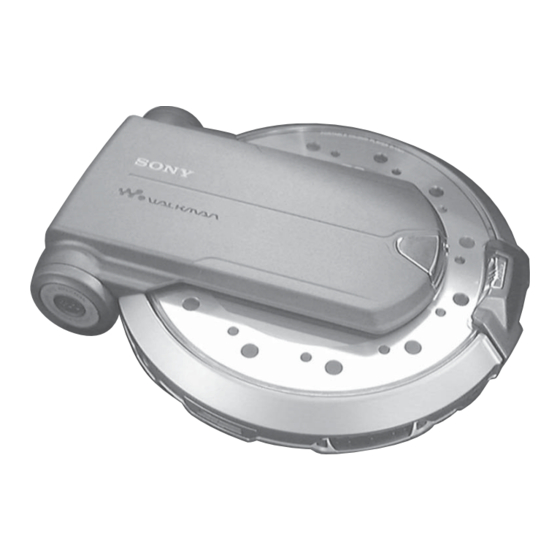
PORTABLE CD/DVD PLAYER
US Model
Canadian Model
AEP Model
UK Model
E Model
Chinese Model
Tourist Model
CDM-501
Advertisement
Table of Contents

Related Manuals for Sony D-VM1


Summary of Contents for Sony D-VM1
-
Page 1: Specifications
332 g (11.7 oz) (player only), 571 g (1 lb 4 oz) (with rechargeable battery) PORTABLE CD/DVD PLAYER Operating temperature 5°C to 35°C Operating humidity 25% to 80% Sony Corporation 9-873-411-03 2002D1600-1 Personal Audio Company © 2002.04 Published by Sony Engineering Corporation... -
Page 2: Table Of Contents
CRITIQUES POUR LA SÉCURITÉ DE FONCTIONNEMENT. NE COMPONENTS WITH SONY PARTS WHOSE PART NUMBERS REMPLACER CES COMPOSANTS QUE PAR DES PIÈSES SONY APPEAR AS SHOWN IN THIS MANUAL OR IN SUPPLEMENTS DONT LES NUMÉROS SONT DONNÉS DANS CE MANUEL OU PUBLISHED BY SONY. - Page 3 D-VM1 On cleaning Self-diagnosis Function • Fingerprints or dust on a disc may cause deteriorated image or sound quality. Leave (When letters/numbers appear in the the disc clean. display) • Wipe the disc with a soft cloth from the center out.
-
Page 4: Servicing Note
D-VM1 SECTION 1 SERVICING NOTE Note: If you are going to repair the monitor unit. NOTES ON HANDLING THE OPTICAL PICK-UP Do not touch the inverter unit and piezo-electric transformer that BLOCK OR BASE UNIT are mounted on the TFT board both in the statuses of power-on and power-off. -
Page 5: General
D-VM1 SECTION 2 GENERAL This section is extracted from instruction manual. A OPEN knob Player (remote sensor) C CHG (charge) indicator D POWER indicator E HOLD switch F VOL (volume) +/– buttons The VOL + button has a tactile dot. - Page 6 D-VM1 A SHIFT button Monitor unit B BRIGHT knob i (headphones) jack The buttons on the monitor unit work HOLD switch differently when they are operated with the E ./> (previous/next) buttons SHIFT button. When operated with SHIFT: Slow motion/One frame playback buttons F VOL (volume) +/–...
-
Page 7: Disassembly
D-VM1 SECTION 3 DISASSEMBLY Note : Disassemble the unit in the order as shown below. Inverter unit, TFT board, Monitor unit section Cabinet (rear), Connection coard (monitor) Liquid crystal indicator display (LCD901) Main section Lid (disc) Cabinet (upper) CDM501, Main board... - Page 8 D-VM1 3-2. INVERTER UNIT, TFT BOARD, LIQUID CRYSTAL INDICATOR DISPLAY (LCD901) Connector, 3pin (Inverter unit) Connector, 24pin (CN1401) 4 Two screws ( + BM1.7 × 6) Inverter unit Remove the six soldrings. TFT board, complete Spacer (M) Knob (Direction key M)
- Page 9 D-VM1 3-4. CABINET (UPPER) 1 Ten screws ( + BM1.7 × 6) screw, tapping 4 Cabinet (Upper) 3-5. CDM501, MAIN BOARD CDM501 Main board, complete Connector, 30pin (CN601) Connector, 8pin (CN1601) Cabinet (Lower)
- Page 10 D-VM1 3-6. BUCKLE Stopper (Shaft) Two screws, tapping Two claws Shaft (Buckle) Cabinet (Lower) Lever (Battery direction) Press the two shafts (buckles) that are located in the recessed areas in the right and left of the cabinet (lower) in the direction of the arrows respectively.
-
Page 11: Test Mode
D-VM1 SECTION 4 TEST MODE Note : About “R” As this unit has only a few buttons, some operations require the use of remote commander (RMT-DV20/provided with unit: 1-476-993-11) buttons. These operations are indicated as “R” in this manual. Example: ...Press the... - Page 12 Ad- Model Type dress and Data when reading. The following display, for ex- D-VM1 (HK) ample, shows the data 0xA55A was read from address D-VM1 (JE) 0x00080000 though it was written to the address 0x00000000.
- Page 13 D-VM1 (5-5) ARP RAM Check Check Items List Data write → read, and accord check Error 11 : ARP RAM read data discord 2. Version (Version Display) The program code data stored in ROM are copied to all areas (2-2) Revision...
- Page 14 D-VM1 4-4. DRIVE AUTO ADJUSTMENT 1. DVD-SL (single layer) Select 1 “R” and insert DVD single layer disc, and press the On the Test Mode Menu screen, press 1 “R” key on the remote ENTER “R” key, and the adjustment will be made through the commander, and the drive auto adjustment menu will be displayed.
- Page 15 D-VM1 3. DVD-DL (dual layer) 4. SACD (SACD hybrid layer) Select 3 “R” , insert the DVD dual layer disc, and press the Select 4 “R” , insert the SACD disc, and press the ENTER “R” ENTER “R” key, and the adjustment will be made through the...
- Page 16 D-VM1 4-5. DRIVE MANUAL OPERATION 0. Disc Check Memory On the Test Mode Menu screen, select 2 “R” , and the Manual operation menu will be displayed. For the Manual operation, each Disc Check servo on/off control and adjustment can be executed manually.
- Page 17 D-VM1 Display when DVD SL 12cm disc was selected 2. Servo Control 1. Disc Type Auto Check [DVD SL] 2. 12 cm 8 cm Servo Control [DVD DL] 3. 12 cm 8 cm 1. LD Off R.Sled FWD [CD] 12cm 8 cm 2.
- Page 18 D-VM1 4-7. EMERGENCY HISTORY 6. Memory Check ### EMG. History ### EEPROM Data1 -– CD –- -– DVD –- SL L0 L1 ID No.XX Laser Hours xxxxxxxh Fcs Gain xx xx xx xx xx xx xxxxxxxh TRK. Gain xx xx xx...
- Page 19 D-VM1 Emergency Codes List 4-9. VIDEO LEVEL ADJUSTMENT 10: Communication to IC001 (RF-240 board) failed. On the Test Mode Menu screen, selecting 6 “R” displays color 11: Each servo for focus, tracking, and spindle is unlocked. bars for video level adjustment. During display of color bars, OSD 12: Communication to EEPROM and IC1102 failed.
- Page 20 D-VM1 4-11-4. START-UP CONFIRMATION DISPLAY OF POWER (CHARGE) TEST MODE • Main unit LED display : POWER (Orange LED) (Green LED or Red LED) • On the CHG LED (orange LED) While detecting the charging status (6 hours or 1 minutes) : LED turns on.
-
Page 21: Diagrams
D-VM1 SECTION 5 DIAGRAMS NOTE FOR PRINTED WIRING BOARDS AND SCHEMATIC DIAGRAMS • WAVEFORMS TFT BOARD Note on Printed Wiring Board Note on Schematic Diagram: IC1404 eh (G OUT) IC1404 es (B OUT) • X : parts extracted from the component side. -
Page 22: Block Diagram - Rf/Servo Section
D-VM1 5-1. BLOCK DIAGRAM – RF/SERVO SECTION – IC1602(1/2) IC1003 IC1002 FOCUS/TRACKING DRAM IC601 OPTICAL PICK-UP BLOCK COIL DRIVE IC1605(1/2) FCD– B(DVD) SSCK OUT1A ERR1 SCLK FCD+ A(DVD) OUT1B D(DVD) MA0-9 OUT2A MA0-9 C(DVD) SSDATA OUT1B SDATA MD00-15 IC1605(2/2) TRD–... -
Page 23: A/V, Syscon Section
D-VM1 – A/V, SYSCON SECTION – IC902 IC1105 A/V DEC. 16M FLASH MEMORY WIDE ACH12 V_OUT ACH12 COMPOUT VIDEO OUT,IF-COM ACH34 Y_OUT ACH34 YOUT BLOCK ACH56 C_OUT HD0-HD15 ACH56 COUT SPDIF1 IC1104 AUDIO SCLK G OUT BCK0 SYSTEM CONTROL CR-B... -
Page 24: Audio Section
D-VM1 – AUDIO SECTION – IC1201 AUDIO DSP IC304 ACH12 LINE AMP SDI0 ACH34 A/V DEC. SDI1 SD00 LINER ACH56 SYSTEM CONTROL SDI2 BLOCK Q103,203 384FS EXTAL MUTE LRCK VIDEO OUT, SCLK IF-COM SCKR LINEL BLOCK IC1202 SCKT Q101, A/V DEC. -
Page 25: Video Out Section
D-VM1 – VIDEO OUT SECTION – CN501 CR-B TFT+B POWER CB-Y BLOCK HPCOM SPDIF CN502 AUDIO LINEL Q501,506 BLOCK IC501 AUDIO VIDEO AMP LINER VIDEO BLOCK VIDEOV DOUT OUTA1 COUT OUTA2 VIDEOY Q502,507 A/D DEC., OUTB1 CR-B SYSTEM CONTROL VIDEO... -
Page 26: Power Section
D-VM1 – POWER SECTION – IC405 TFT+B DC/DC CONVERTER VIDEO OUT, IF-COM L406 BLOCK Q404 SWITCH D409 D406 D405 OUT-1 SCP-1 UNREG INV-1 L412 VIDEO OUT, IF-COM BLOCK LF401 J401 L411 L405 Q409 DC IN 10V SWITCH OUT-2 SCP-2 INV-2... -
Page 27: Tft Section
D-VM1 – TFT SECTION – CN1302 HPCOM J1301 IC1404 TFT DRIVER, TIMING GENERATOR IC1407 EN_DM1 EEPROM CN1401 SI2_EA0 TFT PANEL SCK2_ECL MODULE WIDE (LCD901) WIDE DT_DM2 SDAT HCK2 VIDEO OUT, HCK2 IF-COM HCK1 HCK1 BLOCK GREEN G OUT R OUT... -
Page 28: Printed Wiring Board - Main Section (Side A) (Over All View)
D-VM1 5-2. PRINTED WIRING BOARD – MAIN SECTION (SIDE A) (OVER ALL VIEW) – MAIN BOARD • Semiconductor IC1605 Location Ref. No. Location Ref. No. Location D103 Q101 D104 Q102 IC1606 D203 Q103 D204 Q201 D301 Q202 D302 Q203 D303... -
Page 29: Printed Wiring Board - Main Section (Side A) (1/4)
D-VM1 5-3. PRINTED WIRING BOARD – MAIN SECTION (SIDE A) (1/4) – • : Uses unleaded solder. MAIN BOARD • Semiconductor Location Ref. No. Location Ref. No. Location D103 Q101 D104 Q102 D203 Q103 D204 Q201 D301 Q202 D302 Q203... -
Page 30: Printed Wiring Board - Main Section (Side A) (2/4)
D-VM1 5-4. PRINTED WIRING BOARD – MAIN SECTION (SIDE A) (2/4) – • : Uses unleaded solder. • Semiconductor Location Ref. No. Location Ref. No. Location D103 Q101 D104 Q102 D203 Q103 D204 Q201 D301 Q202 D302 Q203 D303 Q301... -
Page 31: Printed Wiring Board - Main Section (Side A) (3/4)
D-VM1 5-5. PRINTED WIRING BOARD – MAIN SECTION (SIDE A) (3/4) – • : Uses unleaded solder. LIMIT NORMAL S 4 0 1 • Semiconductor (BAT DET) Location Ref. No. Location Ref. No. Location S2011 NTSC/PAL D103 Q101 D104 Q102... -
Page 32: Printed Wiring Board - Main Section (Side A) (4/4)
D-VM1 5-6. PRINTED WIRING BOARD – MAIN SECTION (SIDE A) (4/4) – • : Uses unleaded solder. 1 2 0 • Semiconductor Location R 1 1 5 0 Ref. No. Location Ref. No. Location D103 Q101 D104 Q102 D203 Q103... -
Page 33: Printed Wiring Board - Main Section (Side B) (Over All View)
D-VM1 5-7. PRINTED WIRING BOARD – MAIN SECTION (SIDE B) (OVER ALL VIEW) – (SIDE B) MAIN BOARD IC1004 SPINDLE MOTOR • Semiconductor M901 Location SLED OPTICAL PICKUP IC1002 MOTOR BLOCK Ref. No. Location CSP(Chip Size Package) INLIM D405 SWITCH... -
Page 34: Printed Wiring Board - Main Section (Side B) (1/4)
D-VM1 5-8. PRINTED WIRING BOARD – MAIN SECTION (SIDE B) (1/4) – • : Uses unleaded solder. (SIDE B) MAIN BOARD • Semiconductor S 2 0 1 2 Location HOLD Ref. No. Location D405 D406 D407 D408 SPINDLE D409 MOTOR... -
Page 35: Printed Wiring Board - Main Section (Side B) (2/4)
D-VM1 5-9. PRINTED WIRING BOARD – MAIN SECTION (SIDE B) (2/4) – • : Uses unleaded solder. S 2 0 0 4 S 2 0 0 5 S 2 0 0 2 • Semiconductor Location S 2 0 0 3 Ref. -
Page 36: Printed Wiring Board - Main Section (Side B) (3/4)
D-VM1 5-10. PRINTED WIRING BOARD – MAIN SECTION (SIDE B) (3/4) – • : Uses unleaded solder. • Semiconductor Location Ref. No. Location D405 D406 D407 D408 D409 D410 D412 D413 D416 D508 D510 D511 D515 D516 D1601 D1602 D2004... -
Page 37: Printed Wiring Board - Main Section (Side B) (4/4)
D-VM1 5-11. PRINTED WIRING BOARD – MAIN SECTION (SIDE B) (4/4) – • : Uses unleaded solder. R 1 6 0 2 • Semiconductor Location DOWNLOAD Ref. No. Location D405 D406 D407 D408 D409 D410 DIAG JIG D412 D413 D416... -
Page 38: Schematic Diagram - Main Section (1/11)
D-VM1 • See page 21 for Wavefoms. • See page 56 for IC Block Diagram. 5-12. SCHEMATIC DIAGRAM – MAIN SECTION (1/11) – (Page 45,48) (Page 41) (Page 40) IC B/D (Page 40) (Page 40) (Page 43,47) (Page 40,48) (Page 43) -
Page 39: Schematic Diagram - Main Section (2/11)
D-VM1 5-13. SCHEMATIC DIAGRAM – MAIN SECTION (2/11) – • See page 21 for Wavefoms. • See page 57 for IC Block Diagram. (Page 38) M901 (Page 40) (Page 40) (Page 43) IC B/D (Page 40,41,42,43) (Page 48) (Page 40) -
Page 40: Schematic Diagram - Main Section (3/11)
D-VM1 5-14. SCHEMATIC DIAGRAM – MAIN SECTION (3/11) – (Page 39) (Page 38) (Page 38) (Page 39) (Page 38) (Page 41) (Page 38) (Page 41,42,43) (Page 41,42,43) (Page 38) (Page 41,42,43) (Page 43) (Page 38,48) (Page 39) (Page 39,41,42,43) (Page 39) -
Page 41: Schematic Diagram - Main Section (4/11)
D-VM1 5-15. SCHEMATIC DIAGRAM – MAIN SECTION (4/11) – (Page42,45,46,47,48) 2SJ053600LS0 (Page42,45,48) (Page39,40,42,43) (Page 38) (Page43) (Page42) (Page43) (Page43) (Page 39) (Page42,43) (Page 40) (Page 40,42,43) (Page 40,42,43) (Page 40,42,43) (Page43) -
Page 42: Schematic Diagram - Main Section (5/11)
D-VM1 5-16. SCHEMATIC DIAGRAM – MAIN SECTION (5/11) – (Page 43) (Page 40,41,43)(Page 40,41,43) (Page 41,43) (Page 41,45,46,47,48) (Page 48) (Page 43) (Page 43) (Page 43) (Page 43) (Page 43) (Page 39,40,41,43) R924 (Page 40,41,43) (Page 44) (Page 44,45) (Page 46) -
Page 43: Schematic Diagram - Main Section (6/11)
D-VM1 5-17. SCHEMATIC DIAGRAM – MAIN SECTION (6/11) – • See page 21 for Wavefoms. • See page 54 for IC Block Diagram. • See page 59 for IC Pin Function Description. (Page 40) (Page 41) (Page 45) (Page 39) -
Page 44: Schematic Diagram - Main Section (7/11)
D-VM1 5-18. SCHEMATIC DIAGRAM – MAIN SECTION (7/11) – (Page 42,45) (Page 42) (Page 43) (Page 43) (Page 45) (Page 43,45) -
Page 45: Schematic Diagram - Main Section (8/11)
D-VM1 5-19. SCHEMATIC DIAGRAM – MAIN SECTION (8/11) – • See page 54 for IC Block Diagram. (Page 38,48) IC B/D (Page 44) (Page 43) (Page46) (Page 42,44) (Page 43) (Page 43,44) (Page47) (Page47) (Page 43) IC B/D (Page 41,42,48) -
Page 46: Schematic Diagram - Main Section (9/11)
D-VM1 • See page 21 for Wavefoms. 5-20. SCHEMATIC DIAGRAM – MAIN SECTION (9/11) – (Page 41, 42, 45,47) (Page 42) (Page 47) (Page 48) (Page 47) (Page 47) (Page 42) (Page 45) (Page 47) (Page 48) (Page 43) (Page 48) -
Page 47: Schematic Diagram - Main Section (10/11)
D-VM1 5-21. SCHEMATIC DIAGRAM – MAIN SECTION (10/11) – • See page 21 for Wavefoms. • See page 61 for IC Pin Function Description. NTSC/PAL NTSC (Page 45) (Page 45) (Page 43) (Page 46) (Page 46) (Page 48) (Page 43,48) -
Page 48: Schematic Diagram - Main Section (11/11)
D-VM1 • See page 21 for Wavefoms. • See page 54, 55 for IC Block Diagram. 5-22. SCHEMATIC DIAGRAM – MAIN SECTION (11/11) – (Page 47) (Page 46) (Page 41,42,45,46) (Page 41,42,45) IC B/D (Page 38,40) (Page 47) IC B/D... -
Page 49: Printed Wiring Board - Tft Section (Side A)
D-VM1 5-23. PRINTED WIRING BOARD – TFT SECTION (SIDE A) – • : Uses unleaded solder. TFT BOARD (SIDE A) RV1401 S3002 SHIFT R V 1 3 0 1 IC1404 RV1302 BRIGHT • Semiconductor IC1402 Location Ref. No. Location D1302... -
Page 50: Printed Wiring Board - Tft Section (Side B)
D-VM1 5-24. PRINTED WIRING BOARD – TFT SECTION (SIDE B) – • : Uses unleaded solder. TFT BOARD (SIDE B) S3003 S3004 S3005 S3007 ENTER S3006 POWER S3008 S1301 HOLD (LID) 1-683-218- (11) • Semiconductor Location Ref. No. Location D3001... -
Page 51: Schematic Diagram - Tft Section (1/3)
D-VM1 5-25. SCHEMATIC DIAGRAM – TFT SECTION (1/3) – (Page 52) 330 H RV1301 3.3k 330k (Page 53) R1303 0 (Page 46) (Page 52) I N V E R T E R U N I T ( L I D ) -
Page 52: Schematic Diagram - Tft Section (2/3)
D-VM1 5-26. SCHEMATIC DIAGRAM – TFT SECTION (2/3) – SML-310LTT86 (Page 51) -
Page 53: Schematic Diagram - Tft Section (3/3)
D-VM1 5-27. SCHEMATIC DIAGRAM – TFT SECTION (3/3) – • See page 21 for Wavefoms. • See page 58 for IC Block Diagram. IC B/D (Page 51) -
Page 54: Ic Block Diagrams
D-VM1 IC401 MB3833APFV-G-BND-ER (MAIN BOARD) 5-28. IC BLOCK DIAGRAMS IC301 CXD9627A-E2 (MAIN BOARD) VIN1 CLOCK MCLK DZFL ¥25 DIVIDER DZER DE-EMPHASIS CONTROL -IN2 -IN1 ∆Σ AOUTL+ BICK MODULATOR INTERPOLATOR AOUTL- AUDIO SDTI DATA INTERFACE ∆Σ AOUTR+ LRCK MODULATOR INTERPOLATOR AOUTR- µP... - Page 55 D-VM1 IC405 BA9737KV-E2 (MAIN BOARD) VCC-12 DTC-2 TIMER BIAS-2 STB-1 VOLTAGE LATCH REFERENCE BIAS-1 CAP-H2 STB-2 DTC-1 CAP-H1 INV-1 CAP-L1 NON-1 CAP-L2 FB-1 OUT-1 VCC-12 SCP-1 OUT-2 BIAS-2 DTC-2 CAP-H2 INV-2 CAP-L2 P-GND VREF FB-2 OUT-2 SCP-2 BIAS-3 BIAS-3 DTC-3...
- Page 56 D-VM1 IC601 SSI33P3721-R4 (MAIN BOARD) 62 61 60 59 54 53 52 51 SEL INT OUTPUT INHIBIT FROM S-PORT DVDRFP PROGRAMMABLE INPUT DVDRFN EQUALIZER BIAS FILTER AGC CHARGE FULL WAVE INPUT INPUT RECTIFIER PUMP IMPEDANCE SEL IMPEDANCE SEL FROM S-PORT...
- Page 57 D-VM1 IC1602 MPC17A51/ZVMEL (MAIN BOARD) LOW VOLTAGE DETECTOR CHAGE DGND PUMP VIN12 ERR 1 MOTOR DRIVER CH 1 VIN12 VIN34 VIN12 SAWTOOTH VIN34 OUT 1 A OUT 1 A OUT 3 A OUT 1 B PGND1 PGND3 VIN12 OUT 1 B...
- Page 58 D-VM1 IC1404 CXA3268AR (TFT BOARD)1 PSIG- G OUT PSIG- OSD RGB BRIGHT TST11 G DC OUT FILTER CONTRAST USER-BRIGHT POL SW CONT U-BRT OSD B R OUT TRAP GAMMA FILTER γ1 γ2 WHITLIM BIAS OSD R R DC DET SUB-CONT R...
-
Page 59: Ic Pin Function Descriptions
D-VM1 5-29. IC PIN FUNCTION DESCRIPTIONS • IC1104 MB91107PFV-G-BND (SYSTEM CONTROL) Pin No. Pin Name Description 1 to 5 HA17 - HA21 Address bus HA22 Address bus (Not used) FRSLP Stop mode operating condition signal output (FR SLEEP) WIDE Monitor setting signal output (WIDE-NORMAL) AVCC –... - Page 60 D-VM1 Pin No. Pin Name Description XVPRST Reset signal output to the VPT CHMOD Mode setting signal output to the VPT VRCS Chip select signal output to the HPVR 44.1/48K Clock selection signal output for DVD/CD MAMUTE Main audio muting signal output...
- Page 61 D-VM1 • IC2002 M38869M8A-120HP (INTERFACE MICROCOMPUTER) Pin No. Pin Name Description MONKEY0 Key on the monitor unit signal input XFRST Reset signal output to the system controller XFRON Power control signal output to the system controller MONCNT Monitor backlight control signal output...
- Page 62 D-VM1 Pin No. Pin Name Description XHOLD HOLD switch on the main unit signal input NTSCXPAL NTSC/PAL switch on the main unit signal input XSLPWR Sleep power supply control signal output XFRWAKE Backup data clear request signal output to the system controller...
-
Page 63: Exploded Views
D-VM1 Ver 1.2 2002.04 SECTION 6 EXPLODED VIEWS NOTE: • -XX, -X mean standardized parts, so they may • The mechanical parts with no reference number The components identified by mark 0 or have some differences from the original one. - Page 64 D-VM1 Ver 1.2 2002.04 6-2. CABINET (UPPER) SECTION supplied supplied supplied Ref. No. Part No. Description Remarks Ref. No. Part No. Description Remarks 3-236-378-11 SCREW (M1.4), STEP 3-238-145-01 LABEL, LENS CAUTION 3-236-378-01 SCREW (M1.4), STEP 3-236-344-01 CABINET (UPPER) (EXCEPT CH,HK,JE)
- Page 65 D-VM1 Ver 1.2 2002.04 6-3. CABINET (LOWER) SECTION supplied M901 supplied 105 106 Ref. No. Part No. Description Remarks Ref. No. Part No. Description Remarks 3-236-366-01 SHAFT (BUCKLE) 3-236-356-11 CABINET (LOWER) (AEP,UK,FR) 3-236-361-01 BUCKLE 3-236-356-21 CABINET (LOWER) (HJ,JE) 3-236-365-01 LEVER (LOCK)
-
Page 66: Electrical Parts List
D-VM1 Ver 1.2 2002.04 SECTION 7 MAIN ELECTRICAL PARTS LIST NOTE: • RESISTORS • SEMICONDUCTORS • Due to standardization, replacements in the All resistors are in ohms. In each case, u: µ, for example: parts list may be different from the parts METAL: metal-film resistor uA...: µA... - Page 67 D-VM1 MAIN Ref. No. Part No. Description Remarks Ref. No. Part No. Description Remarks C452 1-104-851-11 TANTAL. CHIP 10uF 20.00% 10V C621 1-125-777-11 CERAMIC CHIP 0.1uF 10.00% 10V C453 1-165-845-21 TANTAL. CHIP 47uF 6.3V C622 1-125-837-11 CERAMIC CHIP 6.3V C455 1-165-845-21 TANTAL.
- Page 68 D-VM1 MAIN Ref. No. Part No. Description Remarks Ref. No. Part No. Description Remarks C919 1-164-943-11 CERAMIC CHIP 0.01uF 10.00% 16V C1112 1-164-943-11 CERAMIC CHIP 0.01uF 10.00% 16V C920 1-164-943-11 CERAMIC CHIP 0.01uF 10.00% 16V C1113 1-125-777-11 CERAMIC CHIP 0.1uF 10.00% 10V...
- Page 69 D-VM1 MAIN Ref. No. Part No. Description Remarks Ref. No. Part No. Description Remarks C1643 1-125-777-11 CERAMIC CHIP 0.1uF 10.00% 10V D407 8-719-072-43 DIODE RB050L-40TE25 C1644 1-125-777-11 CERAMIC CHIP 0.1uF 10.00% 10V D408 8-719-072-43 DIODE RB050L-40TE25 C1645 1-164-346-11 CERAMIC CHIP...
- Page 70 D-VM1 MAIN Ref. No. Part No. Description Remarks Ref. No. Part No. Description Remarks < IC > < COIL > IC301 6-701-565-01 IC CXD9627A-E2 L302 1-414-398-11 INDUCTOR 10uH IC302 8-749-014-79 IC LM2664M6X L303 1-414-754-11 INDUCTOR 10uH IC303 8-759-422-21 IC NJM4580V(TE2)
- Page 71 D-VM1 MAIN Ref. No. Part No. Description Remarks Ref. No. Part No. Description Remarks Q404 8-729-048-75 TRANSISTOR CPH3109-TL-E R123 1-218-990-11 SHORT Q405 8-729-029-14 TRANSISTOR DTC144EUA-T106 R124 1-218-957-11 RES-CHIP 2.2K 1/16W Q406 8-729-028-76 TRANSISTOR DTA114YUA-T106 R127 1-218-973-11 RES-CHIP 1/16W Q407 8-729-048-75 TRANSISTOR...
- Page 72 D-VM1 MAIN Ref. No. Part No. Description Remarks Ref. No. Part No. Description Remarks R421 1-218-990-11 SHORT R501 1-218-990-11 SHORT R422 1-218-990-11 SHORT R502 1-218-990-11 SHORT R424 1-218-990-11 SHORT R503 1-218-990-11 SHORT R425 1-218-967-11 RES-CHIP 1/16W R504 1-218-990-11 SHORT R426...
- Page 73 D-VM1 MAIN Ref. No. Part No. Description Remarks Ref. No. Part No. Description Remarks R617 1-208-695-11 METAL CHIP 3.3K 0.5% 1/16W R724 1-218-941-11 RES-CHIP 1/16W R618 1-208-707-11 METAL CHIP 0.5% 1/16W R729 1-208-643-11 RES-CHIP 1/16W R619 1-208-699-11 METAL CHIP 4.7K 0.5%...
- Page 74 D-VM1 MAIN Ref. No. Part No. Description Remarks Ref. No. Part No. Description Remarks R1031 1-218-965-11 RES-CHIP 1/16W R1168 1-218-977-11 RES-CHIP 100K 1/16W R1033 1-218-965-11 RES-CHIP 1/16W R1171 1-218-941-11 RES-CHIP 1/16W R1034 1-218-965-11 RES-CHIP 1/16W R1181 1-218-941-11 RES-CHIP 1/16W R1036...
- Page 75 D-VM1 MAIN Ref. No. Part No. Description Remarks Ref. No. Part No. Description Remarks R1633 1-218-961-11 RES-CHIP 4.7K 1/16W R2069 1-218-990-11 SHORT R1634 1-218-965-11 RES-CHIP 1/16W R2072 1-218-990-11 SHORT R1635 1-218-965-11 RES-CHIP 1/16W R2074 1-218-990-11 SHORT R1636 1-218-979-11 RES-CHIP 150K...
- Page 76 D-VM1 Ver 1.2 2002.04 MAIN Ref. No. Part No. Description Remarks Ref. No. Part No. Description Remarks S2005 1-786-278-11 SWITCH, TACTILE (VOL-) C1414 1-164-940-11 CERAMIC CHIP 0.0033uF 10.00% 16V S2011 1-553-977-00 SWITCH, SLIDE (NTSC/PAL) C1415 1-125-837-11 CERAMIC CHIP 6.3V S2012 1-572-922-11 SWITCH, SLIDE (HOLD .)
- Page 77 D-VM1 Ref. No. Part No. Description Remarks Ref. No. Part No. Description Remarks < JACK > R1414 1-208-719-11 METAL CHIP 0.5% 1/16W R1416 1-208-635-11 RES-CHIP 1/16W J1301 1-784-943-51 JACK (SMALL TYPE) (i) R1417 1-208-711-11 METAL CHIP 0.5% 1/16W R1418 1-218-969-11 RES-CHIP 1/16W <...
- Page 78 D-VM1 Ver 1.2 2002.04 Ref. No. Part No. Description Remarks Ref. No. Part No. Description Remarks < VARIABLE RESISTOR > ACCESSORIES ************ RV1301 1-225-905-11 RES, ADJ, CERMET (3 TYPE) 47K RV1302 1-227-446-11 RES, VAR, CARBON 2K (BRIGHT 1-418-889-11 ADAPTOR, AC (HK)