Table of Contents
Advertisement
Advertisement
Chapters
Table of Contents
Troubleshooting

Related Manuals for Motorola Professional GP340


Summary of Contents for Motorola Professional GP340
- Page 1 Professional Radio GP Series Detailed Service Manual 6866558D04-O...
- Page 3 Professional Radio GP Series Detailed Service Manual 6866558D04-O Contents Section 1 Service Maintainability Section 2 Keypad Service Information Section 3 Power Distribution and Controller Information Section 4 VHF Service Information Section 5 300R1 Service Information Section 6 Lowband Service Information KTT EMEA Publications Department, Jays Close, Viables Industrial Estate, Basingstoke, Hampshire, RG22 4PD, UK.
-
Page 5: Safety Information
Read this information before using the radio. PRODUCT SAFETY AND RF EXPOSURE FOR PORTABLE TWO-WAY RADIOS. This document provides information and instructions for the safe and efficient operation of Motorola Portable Two-Way Radios. The information provided in this document supersedes information contained in user guides published prior to February 2002. -
Page 6: Rf Exposure Compliance And Control Guidelines And Operating Instructions
Compliance with RF Exposure Standards Your Motorola two-way radio is designed and tested to comply with a number of national and International standards and guidelines (listed below) for human exposure to radio frequency electromagnetic energy. This radio complies with the IEEE (FCC) and ICNIRP exposure limits for occupational/controlled RF exposure environments at operating duty factors of up to 50% talk- 50% listen and is authorized by the IEEE/ICNIRP for occupational use only. - Page 7 Motorola - approved antennas, batteries and accessories may exceed IEEE/ICNIRP RF exposure guidelines. For a list of Motorola-approved antennas, batteries, and other accessories please see your dealer or local Motorola contact. Your nearest dealer can be found at the following web site: http://www.motorola.com/cgiss/emea/dealerlocator.html Additional Information For additional information on exposure requirements or other training information, visit http://www.motorola.com/rfhealth.
-
Page 8: Medical Devices
viii ELECTROMAGNETIC INTERFERENCE/COMPATIBILITY NOTE: Nearly every electronic device is susceptible to electromagnetic interference (EMI) if inadequately shielded, designed or otherwise configured for electromagnetic compatibility. Facilities To avoid electromagnetic interference and/or compatibility conflicts, turn off your radio in any facility where posted notices instruct you to do so. Hospitals or health care facilities may be using equipment that is sensitive to external RF energy. -
Page 9: Operational Warnings
OPERATIONAL WARNINGS Vehicles with an air bag Refer to vehicle manufacturer's manual prior to installation of electronic equipment to avoid interference with air bag wiring. WARNING: Do not place a portable radio in the area over an air bag or in the air bag deployment area. -
Page 10: Intrinsically Safe Radio Information
Warnings for Radios Approved as Intrinsically Safe Radios must ship from the Motorola manufacturing facility with the hazardous atmosphere capability and the intrinsic safety approval labelling (FM, UL, CSA, CENELEC or ATEX). Radios will not be upgraded to this capability and labeled once they have been shipped to the field. - Page 11 The manual PN referenced on the Intrinsically Safe Approval Label identifies the approved Accessories and or options that can be used with that portable radio unit. Using a non Motorola intrinsically safe battery and or accessory with the Motorola approved radio unit will void the intrinsically safe approval of that radio unit.
- Page 13 Professional Radio GP Series 300R1 (300 - 350MHz) Service Information Issue: November 2004...
- Page 14 Accordingly, any copyrighted Motorola computer programs contained in the Motorola products described in this manual may not be copied or reproduced in any manner without the express written permission of Motorola. Furthermore, the purchase of Motorola...
-
Page 15: Table Of Contents
Table of Contents Chapter 1 MODEL CHART AND TECHNICAL SPECIFICATIONS 1.0 GP340 Model Chart .....................1-1 2.0 GP640 / GP680 Model Chart ................1-1 3.0 Technical Specifications ..................1-2 Chapter 2 THEORY OF OPERATION 1.0 Introduction ......................2-1 2.0 Transmitter......................2-1 2.1 Power Amplifier ....................2-1 2.2 Antenna Switch....................2-2 2.3 Harmonic Filter ....................2-2 2.4 Antenna Matching Network ................2-2... -
Page 17: Chapter 1 Model Chart And Technical Specifications
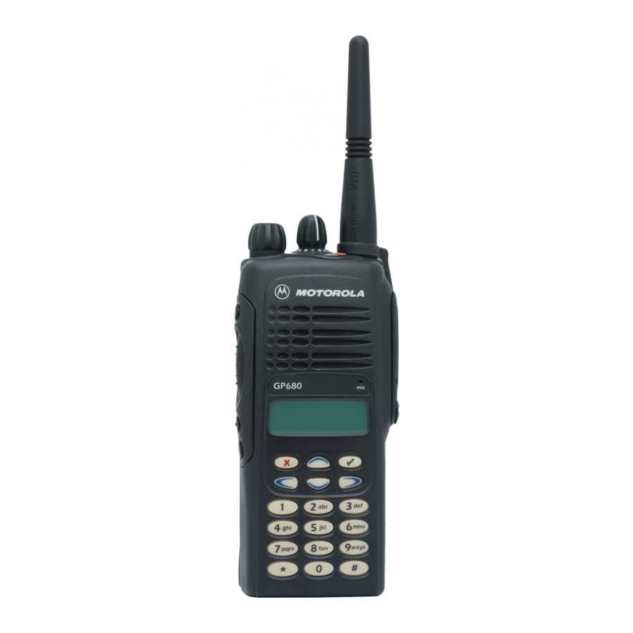
Chapter 1 MODEL CHART AND TECHNICAL SPECIFICATIONS GP340 Model Chart Professional GP300 Series (300-350MHz) Model Description MDH25EDC9AN3_E GP340 300R1 300-350 MHz 4W 16 CH Item Description PMLD4141_ GP340 Back Cover Kit 6864110B13_ GP340 Basic User Guide PMAD4022_ 9cm (300-344 MHz) Antenna HNN9008_ Battery, NiMH Standard x = Indicates one of each is required. -
Page 18: Technical Specifications
MODEL CHART AND TECHNICAL SPECIFICATIONS Technical Specifications Data is specified for +25°C unless otherwise stated. General Specifications Channel Capacity GP340 GP640 16 (Conventional) GP680 16 (Conventional) Power Supply Rechargeable battery 7.5v Dimensions: H x W x D (mm) Height excluding knobs With standard high capacity NiMH battery 137 x 57.5 x 37.5 With ultra high capacity NiMH battery... - Page 19 Technical Specifications Transmitter 300R1 *Frequencies - Full Bandsplit 300-350 MHz Channel Spacing 12.5/20/25 kHz Frequency Stability ±2.5 ppm @ 12.5kHz (-25°C to +55°C, +25° Ref.) ±5ppm @ 25 kHz Power 1-4W ±2.5 @ 12.5 kHz Modulation Limiting ±4.0 @ 20 kHz ±5.0 @ 25 kHz FM Hum &...
- Page 20 MODEL CHART AND TECHNICAL SPECIFICATIONS...
-
Page 21: Chapter 2 Theory Of Operation
Chapter 2 THEORY OF OPERATION Introduction This Chapter provides a detailed theory of operation for the 300-350MHz circuits in the radio. For details of the theory of operation and trouble shooting for the the associated Controller circuits refer to the Controller Section of this manual. Transmitter (Refer to Figure 2-1 and the Transmitter schematic diagram) The transmitter contains five basic circuits:... -
Page 22: Antenna Switch
THEORY OF OPERATION The PRF1507 LDMOS PA is capable of supplying an output power of 7W with an input signal of 0.3W. The current drain would typically be 1300mA while operating in the frequency range of 300-350MHz. The power output can be varied by changing the biasing voltage. Antenna Switch The antenna switch circuit consists of two PIN diodes (CR101 and CR102), a pi network (C107, L104 and C106), and two current limiting resistors (R101, R170). -
Page 23: Receiver
Receiver Receiver Antenna Pin Diode Varactor Varactor Antenna Crystal RF Amp Mixer IF Amp Tuned Filter Tuned Filter Switch RF Jack Filter First LO from FGU Control Voltage from ASFIC Recovered Audio Demodulator Squelch U301 RSSI Synthesizer 16.8 MHz Reference Clock SPI Bus Second LO VCO... -
Page 24: Receiver Back-End
THEORY OF OPERATION Both the pre and post-RF amplifier varactor tuned filters have similar responses. The 3dB bandwidth of the filter is about 50 MHz. This enables the filters to be electronically controlled by using a single control voltage which is DACRx . The output of the post-RF amplifier filter which is connected to the passive double balanced mixer consists of T301, T302 and CR306. -
Page 25: Automatic Gain Control Circuit
Receiver Automatic Gain Control Circuit (Refer to the Receiver Front End and Receiver Back End schematic diagrams) The front end automatic gain control circuit is to provide automatic gain reduction of the front end RF amplifier via feedback. This action is necessary to prevent overloading of backend circuits. This is achieved by drawing some of the output power from the RF amplifier’s output. -
Page 26: Frequency Generation Circuitry
THEORY OF OPERATION Frequency Generation Circuitry (Refer to Figure 2-3 and the Frequency Synthesizer schematic diagram) The Frequency Generation Circuitry is composed of two main ICs, the Fractional-N synthesizer (U201), and the VCO/Buffer IC (U241). Designed in conjunction to maximize compatibility, the two ICs provide many of the functions that normally would require additional circuitry. - Page 27 Frequency Generation Circuitry In achieving fast locking for the synthesizer, an internal adapt charge pump provides higher current at pin 45 of U201 to put synthesizer within the lock range. The required frequency is then locked by normal mode charge pump at pin 43 . Both the normal and adapt charge pumps get their supply from the capacitive voltage multiplier which is made up of C258, C259, C228, triple diode CR201 and level shifters U210 and U211.
-
Page 28: Voltage Controlled Oscillator (Vco)
THEORY OF OPERATION Voltage Controlled Oscillator (VCO) (Refer to Figure 2-5 and the Voltage Controlled Oscillator schematic diagram) The VCOBIC (U241) in conjunction with the Fractional-N synthesizer (U201) generates RF in both the receive and the transmit modes of operation. The TRB line (U241 pin 19) determines which oscillator and buffer will be enabled. - Page 29 Frequency Generation Circuitry Table 2-1 Level Shifter Logic Desired AUX 4 AUX 3 Mode High (@3.2V) High (@4.8V) High Battery Saver Hi-Z/Float (@2.5V) In the receive mode, U241 pin 19 is low or grounded. This activates the receive VCO by enabling the receive oscillator and the receive buffer of U241.
- Page 30 2-10 THEORY OF OPERATION...
-
Page 31: Chapter 3 Troubleshooting Charts
Chapter 3 TROUBLESHOOTING CHARTS Troubleshooting Flow Chart for Receiver (Sheet 1 of 2) START Bad SINAD Bad 20dB Quieting No Recovered Audio udio Check Controller at pin 27 of U301? Spray of inject 1st IF into XTAL Filter IF Freq: 45.1MHz Check Q320 bias circuitry for faults. -
Page 32: Troubleshooting Flow Chart For Receiver (Sheet 2 Of 2)
TROUBLESHOOTING CHARTS Troubleshooting Flow Chart for Receiver (Sheet 2 of 2) Inject RF into J101 Q302 Trace IF signal collector OK? IF Signal from L311 to IF signal at L311? Q302. Check for present? bad XTAL filter. Before replacing U301, check U301 voltages;... -
Page 33: Troubleshooting Flow Chart For Transmitter
Troubleshooting Flow Chart for Transmitter Troubleshooting Flow Chart for Transmitter START No Power Is There B+ Bias for Check Q111 Ant switch CR101 Is Control Voltage Is Current Check PCIC High or Low at C119 High 1. Check Pin Diodes Check Drive to 2. -
Page 34: Troubleshooting Flow Chart For Synthesizer
TROUBLESHOOTING CHARTS Troubleshooting Flow Chart for Synthesizer 3.3V at Check U248, Start U201 pins 5, L201 & L202 20, 34& Check CR201, Visual U210, U211, Correct check of the C258, C259 & Problem Board OK? C228 Is U201 16.8MHz 16.8MHz at pin 6 of Pin47 AT = Replace... -
Page 35: Troubleshooting Flow Chart For Vco
Troubleshooting Flow Chart for VCO Troubleshooting Flow Chart for VCO START No LO? U241 Check R245 TRB = Pin 10 for dry joint 5V? @U241 Carrier? >1V? or faulty Pin 19 VCO OK L253 Change Open L253 Circuit? AUX 3 Check High? R260... - Page 36 TROUBLESHOOTING CHARTS...
- Page 37 Chapter 4 PCB/SCHEMATICS/PARTS LISTS Allocation of Schematics and Circuit Boards Controller Circuits The 300-350MHz circuits are contained on the printed circuit board (PCB) which also contains the Controller circuits. This Chapter shows the schematics for the 300R1 circuits only, refer to the Controller section for details of the related Controller circuits.The PCB component layouts and the Parts Lists in this Chapter show both the Controller and 300R1 circuit components.
- Page 38 PCB/SCHEMATICS/PARTS LISTS...
-
Page 39: Pcb 8485726Z01 - Schematics
PCB 8485726Z01 - Schematics PCB 8485726Z01 - Schematics R410 E408 E407 E409 PB503 PB502 PB504 PB501 R418 VR440 C521 SH323 R300 R352 C397 B504 B503 FL201 RT301 R314 R321 VR501 C328 R335 C363 C325 C362 U405 U406 R338 VR300 J400 R506 R325 L325... - Page 40 PCB 8485726Z01 - Schematics M301 M101 M400 C523 C522 SH402 E405 SH322 C437 L505 E404 L330 VR506 C359 E406 C277 C338 C358 C357 E402 R350 C344 C390 C278 R344 U248 C383 C360 R415 C346 R311 C361 R312 C215 C433 C343 C431 SH202 C208...
- Page 41 PCB 8485726Z01 - Schematics B501 L505 BATTERY_CONTACT 390nH RADIO_CODE 2 DATA UNSWB+ BATT_CODE 1 NEG BATT + F501 3 POS S502 CONN_J SWITCH BATT – MECH_SWB+ LI_ION B503 B504 C502 VR506 CR501 VR439 C503 0.47uF 6.8V 100pF Vdda R507 Vdda C505 6.8V VR501...
- Page 42 PCB 8485726Z01 - Schematics DACRx C322 82pF R342 -59.5dBm@45.1MHz 100K L310 150nH C398 C315 R308 R305 C314 330pF 7.5pF 0.1uF R304 R309 C380 .01uF -52.5dBm@300.01MHz C321 CR306 L304 330pF -53.5dBm@349.99MHz 180nH C306 T301 XFMR 9.1pF C309 C308 330pF R306 R307 330pF 2.285V C312...
- Page 43 PCB 8485726Z01 - Schematics L331 R343 2.20uH Vdd_FILTERED Vdda C382 (SOURCE) 10uF DEMOD R350 C348 C347 C345 C344 C346 100K 0.1uF 0.1uF 0.1uF 0.1uF 0.1uF C390 C329 100pF 0.1uF C343 0.22uF R344 R345 R355 2.628V 3.185V Q320 C342 C357 C384 C383 BFQ67W 56pF...
- Page 44 PCB 8485726Z01 - Schematics U210 C257 U211 TC7ST04FU 330pF C296 C265 TC7ST04FU 0.1uF C258 7.5V .01uF 1.65V U247 ADP3300 C259 SWB+ .01uF CR201 (SOURCE) C294 C293 C291 10uF 330pF 0.47uF 3 K3 A3 4 L202 4V_3.3V U248 2 K2 A2 5 2.2uH L203 LP2980...
- Page 45 PCB 8485726Z01 - Schematics C281 R245 330pF R242 C250 L243 C276 C285 C286 10pF 4.6V 2.2uF 0.1uF 330pF RESONATOR C246 R241 L281 L273 330pF 390nH 22nH C242 9.1pF C272 C273 0.1uF C243 L242 R244 L271 10pF 220nH 82nH RX_INJ C245 2.7pF TX_INJ TX_OUT...
- Page 46 PCB 8485726Z01 - Schematics 4-10 E101 R102 BEAD 0.075 UNSWB+ L107 C114 C123 C108 33.47nH 330pF 10uF 330pF L105 C172 390nH UNSWB+ 0.1uF R106 C109 L106 100pF 10.29nH Microstrip Microstrip R172 C160 L108 C121 L109 L112 100pF 15pF Q110 11.03nH 56nH Microstrip C118...
-
Page 47: Pcb 8485726Z01 - Parts List
PCB 8485726Z01 - Parts List 4-11 PCB 8485726Z01 - Parts List Circuit Motorola Circuit Motorola Circuit Motorola Description Description Description Part No. Part No. Part No. Circuit Motorola Description C204 2104993J02 CAP MONO. CERAMIC (2.2UF) C294 2113743L05 CAP CHIP 330 PF 10% X7R... - Page 48 PCB 8485726Z01 - Parts List 4-12 Circuit Motorola Circuit Motorola Circuit Motorola Circuit Motorola Description Description Description Description Part No. Part No. Part No. Part No. C444 2113743N50 CAP CHIP 100 PF 5% COG CR303 4880154K03 SOT MMBD353 RH DIODE DUAL...
- Page 49 8485726Z01 PC BOARD UHF BAND 3 R407 0662057N19 RES. CHIP 68K 5% 20X40 SH202 2680511Z01 SHIELD, SYNTHESIZER * Motorola Depot Servicing only R409 0662057M98 RES CHIP 10K 5% 20X40 SH241 2680513Z01 SHIELD, VCO TOP Reference designators with an asterisk indicate...
-
Page 50: Pcb 8485726Z04 - Schematics
PCB 8485726Z04 - Schematics 4-14 PCB 8485726Z04 - Schematics R410 E407 E409 R437 PB503 PB502 PB504 PB501 VR440 C521 SH323 R300 R352 C397 FL201 RT301 R314 CR310 R321 VR501 C328 R335 C363 C325 C362 U405 L332 R338 U406 TP201 J400 R506 R325 L325... - Page 51 PCB 8485726Z04 - Schematics 4-15 M301 M101 M400 C523 C522 E404 C437 L505 E406 VR506 L330 C359 C277 S502 C338 C358 Y201 C357 E401 R350 C344 C390 C278 FL401 R344 B501 U248 C383 C360 R311 C346 R415 U301 C525 C215 C361 R312 C433...
- Page 52 PCB 8485726Z04 - Schematics 4-16 RADIO_CODE B501 L505 UNSWB+ BATTERY_CONTACT 390nH DATA BATT_CODE BATT+ F501 BATT- CONN_J S502 MECH_SWB+ SWITCH LI_ION B503 TAB2 B504 C502 VR506 CR501 VR439 C503 TAB1 0.47uF 6.8V 100pF R507 C505 6.8V VR501 100pF Vdda M101 PB501 M100 SWITCH...
- Page 53 PCB 8485726Z04 - Schematics 4-17 DACRx C322 82pF R342 100K L310 150nH C315 R308 R310 R305 C314 100pF 0.1uF R304 C380 R309 .01uF L304 C321 CR306 180nH 100pF C306 T301 XFMR C309 C308 100pF R306 R307 100pF C312 100K 100K C310 C316 C318...
- Page 54 PCB 8485726Z04 - Schematics 4-18 L331 R343 2.20uH Vdd_FILTERED Vdda C382 (SOURCE) 10uF DEMOD R350 C348 C347 C345 C344 C346 100K 0.1uF 0.1uF 0.1uF 0.1uF 0.1uF C390 C329 100pF 0.1uF C343 0.22uF R344 R345 R355 2.628V 3.185V Q320 C342 C357 C384 C383 BFQ67W...
- Page 55 PCB 8485726Z04 - Schematics 4-19 U210 C257 U211 TC7ST04FU 100pF C296 C265 TC7ST04FU 0.1uF C258 .01uF U247 ADP3300 C259 SWB+ .01uF CR201 (SOURCE) C294 C293 C291 10uF 100pF 0.47uF 3 K3 A3 4 4V_3.3V L202 2 K2 A2 5 U248 2.2uH L203 LP2980...
- Page 56 PCB 8485726Z04 - Schematics 4-20 C281 R245 100pF R242 C250 C276 C285 L243 C286 7.5pF 2.2uF 0.1uF 100pF RESONATOR C246 R241 L273 L281 100pF 390nH 39nH C242 7.5pF C272 C273 0.1uF C243 L242 L271 R244 6.8pF 390nH 56nH RX_INJ C245 2.7pF TX_INJ TX_OUT...
- Page 57 PCB 8485726Z04 - Schematics 4-21 E101 BEAD R102 UNSWB+ (91G24) L107 C114 C123 33.47nH 240pF 10uF C172 0.1uF UNSWB+ R106 C109 L106 100pF 7.66nH Microstrip Microstrip R172 TX_OUT L108 L109 C121 C160 L112 (91A11) 11.03nH 100pF 100pF 56nH Microstrip Q110 C118 R175 100pF...
-
Page 58: Pcb 8485726Z04 - Parts List
PCB 8485726Z04 - Parts List 4-22 PCB 8485726Z04 - Parts List Circuit Motorola Circuit Motorola Circuit Motorola Description Description Description Part No. Part No. Part No. Circuit Motorola Description C204 2104993J02 CAP MONO. CERAMIC (2.2UF) C295 2113743N50 CAP CHIP 100 PF 5% COG... - Page 59 PCB 8485726Z04 - Parts List 4-23 Circuit Motorola Circuit Motorola Circuit Motorola Circuit Motorola Description Description Description Description Part No. Part No. Part No. Part No. C444 2113743N50 CAP CHIP 100 PF 5% COG CR251 4862824C01 DIODE VARACTOR IT363 L203...
- Page 60 8485726Z04 PC BOARD UHF BAND 3 R415 0662057V26 RES CHIP 91K 1% 1/16W SH101 2680510Z01 SHIELD, PA * Motorola Depot Servicing only R416 0662057M98 RES. CHIP 10K 5% 20X40 SH201 2680511Z01 SHIELD, SYNTHESIZER Reference designators with an asterisk indicate R418 0662057M01 RES.
- Page 61 Professional Radio GP Series Service Maintainability Issue: November 2004...
- Page 62 Accordingly, any copyrighted Motorola computer programs contained in the Motorola products described in this manual may not be copied or reproduced in any manner without the express written permission of Motorola. Furthermore, the purchase of Motorola...
- Page 63 Table of Contents Chapter 1 INTRODUCTION 1.0 Scope of Manual ....................1-1 2.0 Warranty and Service Support................1-1 2.1 Warranty Period and Return Instructions ............1-1 2.2 After Warranty Period ..................1-1 2.3 European Radio Support Centre (ERSC)............1-2 2.4 Piece Parts .....................1-2 2.5 Technical Support...................1-3 2.6 Related Documents ..................1-3 3.0 Radio Model Information..................1-4 Chapter 2...
-
Page 65: Chapter 1 Introduction
In instances where the product is covered under a "return for replacement" or "return for repair" warranty, a check of the product should be performed prior to shipping the unit back to Motorola. This is to ensure that the product has been correctly programmed or has not been subjected to damage outside the terms of the warranty. -
Page 66: European Radio Support Centre (Ersc)
Aftermarket and Accessory Division (AAD). If no part number is assigned, the part is not normally available from Motorola. If the part number is appended with an asterisk, the part is serviceable by Motorola Depot only. If a parts list is not included, this generally means that no user-serviceable parts are available for that kit or assembly. -
Page 67: Technical Support
Warranty and Service Support Technical Support Motorola Product Services is available to assist the dealer/distributors in resolving any malfunctions which may be encountered. UK/Ireland - Richard Russell France - Lionel Lhermitte Telephone: +44 (0) 1256 488 082 Telephone: +33 1 6929 5722... -
Page 68: Radio Model Information
INTRODUCTION Radio Model Information The model number and serial number are located on a label attached to the back of your radio. You can determine the RF output power, frequency band, protocols, and physical packages. The example below shows one portable radio model number and its specific characteristics. Table 1-1 Radio Model Number (Example: MDH25KDC9AA3AE) Type of Model... -
Page 69: Chapter 2 Maintenance
Chapter 2 MAINTENANCE Introduction This chapter of the manual describes: ❏ preventive maintenance ❏ safe handling of CMOS devices ❏ repair procedures and techniques Preventive Maintenance The radios do not require a scheduled preventive maintenance program; however, periodic visual inspection and cleaning is recommended. Inspection Check that the external surfaces of the radio are clean, and that all external controls and switches are functional. -
Page 70: Safe Handling Of Cmos And Ldmos
When damaged parts are replaced, identical parts should be used. If the identical replacement component is not locally available, check the parts list for the proper Motorola part number and order the component from the nearest Motorola Communications parts center listed in the “Piece Parts”... - Page 71 Chip Components Use either the RLN4062 Hot-Air Repair Station or the Motorola 0180381B45 Repair Station for chip component replacement. When using the 0180381B45 Repair Station, select the TJ-65 mini-thermojet hand piece. On either unit, adjust the temperature control to 370 °C (700 °F), and adjust the airflow to a minimum setting.
- Page 72 MAINTENANCE Shields Removing and replacing shields will be done with the R1070 station with the temperature control set to approximately 215°C (415°F) [230°C (445°F) maximum]. ❏ To remove the shield: Place the circuit board in the R1070 circuit board holder. Select the proper heat focus head and attach it to the heater chimney.
-
Page 73: Notes For All Schematics And Circuit Boards
1. Unless otherwise stated, resistances are in Ohms (k = 1000), and capacitances are in picofarads (pF) or microfarads (µF). 2. DC voltages are measured from point indicated to chassis ground using a Motorola DC multimeter or equivalent. Transmitter measurements should be made with a 1.2 µF choke in series with the voltage probe to prevent circuit loading. - Page 74 MAINTENANCE...
-
Page 75: Chapter 3 Service Aids
Table 3-1 lists the service aids recommended for working on the radio. While all of these items are available from Motorola, most are standard workshop equipment items, and any equivalent item capable of the same performance may be substituted for the item listed. - Page 76 SERVICE AIDS Table 3-2 lists the recommended tools used for maintaining this family of radios. These tools are also available from Motorola.. Table 3-2 Recommended Test Tools Motorola Part Description Application Number 6680702Z01 Chassis opener and knob Disassembly tool removal tool.
-
Page 77: Recommended Test Equipment
Test Equipment Test Equipment Table 3-3 lists test equipment required to service the radio and other two-way radios. Table 3-3 Recommended Test Equipment Motorola Part Description Characteristics Application Number R2600_ Comms System Analyzer This monitor will Frequency/deviation meter and (non MPT). - Page 78 SERVICE AIDS Motorola Part Description Characteristics Application Number * R1440_ Wattmeter, Thruline 50-Ohm, Transmitter power output ±5% accuracy measurements. * 0180305F14 Plug-in Element 10W, 25 - 60MHz * 0180305F29 Plug-in Element 5W, 100-250MHz * 0180305F38 Plug-in Element 5W, 200-500MHz * 0180305F46...
- Page 79 Professional Radio GP Series Keypad and Flex Service Information Issue: November 2004...
- Page 80 Accordingly, any copyrighted Motorola computer programs contained in the Motorola products described in this manual may not be copied or reproduced in any manner without the express written permission of Motorola. Furthermore, the purchase of Motorola...
- Page 81 Table of Contents Chapter 1 THEORY OF OPERATION 1.0 Keypad and Flexible Connectors .................1-1 1.1 Keypad ......................1-1 1.2 Flexible Connectors..................1-1 2.0 Troubleshooting Chart ..................1-2 Chapter 2 PCB / SCHEMATICS / PARTS LISTS 1.0 Allocation of Schematics and Circuit Boards ............2-1 1.1 Flexible Connectors..................2-1 1.2 Keypad PCBs ....................2-1 2.0 PCB/Schematic Diagrams and Parts List: Flexes..........2-3...
-
Page 83: Keypad And Flexible Connectors
Chapter 1 THEORY OF OPERATION Keypad and Flexible Connectors Keypad The keypad block diagram is shown in Figure 1-1. U602 is a comparator that will compare the voltage when any one of the keypad row or keypad column keys is being pressed. Therefore when a key is being pressed, it will send a message to the microprocessor through the output (KEY_INT) telling it that a key has been pressed. -
Page 84: Troubleshooting Chart
THEORY OF OPERATION Troubleshooting Chart Disconnect and Display reconnect 18-pin flex if still Off Disconnect and Keypad reconnect 40-pin flex Figure 1-2 Keypad Board Troubleshooting Chart... -
Page 85: Allocation Of Schematics And Circuit Boards
Chapter 2 PCB / SCHEMATICS / PARTS LISTS Allocation of Schematics and Circuit Boards The printed circuit boards (PCB) and schematic diagrams related to the Flexible Connectors and the Keypads are shown in the tables below: Flexible Connectors Table 2-1: Keypad /Controller Flex Flex : 8480475Z02 Flex... - Page 86 PCB / SCHEMATICS / PARTS LISTS...
-
Page 87: Pcb/Schematic Diagrams And Parts List: Flexes
PCB/Schematic Diagrams and Parts List: Flexes PCB/Schematic Diagrams and Parts List: Flexes Keypad - Controller Flex CONTROLLER KEYPAD J100 J200 EXT_MIC EXT_MIC VS_CS VS_CS SW_B+ SW_B+ <- TO KP Vddd Vddd VS_AUDSEL VS_AUDSEL Det_Aud_Snd Det_Aud_Snd Rx_Aud_Rtn Rx_Aud_Rtn Tx_Aud_Snd Tx_Aud_Snd TO CTRL -> Tx_Aud_Rtn 8480475Z02 REV A Tx_Aud_Rtn... -
Page 88: Universal Connector Flex
PCB/Schematic Diagrams and Parts List: Flexes Universal Connector Flex M400 J404 SPKR_20 J405 J403 J406 20 PIN CONN J407 SPKR_20 J408 J409 J410 J411 J412 INT_SPK+ 13 PIN UNIVERSAL CONN J413 M401 J414 INT_SPK- J415 J416 SPKR_20 EXT_SPKR+ J404 EXT_SPKR+ C402 SPKR_20 EXT_SPK-... -
Page 89: Pcb/Schematic Diagrams And Parts List: Keypad
PCB/Schematic Diagrams and Parts List: Keypad PCB/Schematic Diagrams and Parts List: Keypad PCB 8480574Z06 - Diagram R615 R614 M604 M605 M606 R617 R616 D601 D602 R620 M607 M609 R621 M608 C614 R626 R606 J602 M610 M611 M612 C642 D604 C640 C644 R601 D605 R631... - Page 90 PCB/Schematic Diagrams and Parts List: Keypad Vddd C618 C617 100pF E637 40 PIN CONNECTOR C622 100pF C610 EXT_MIC EXT_MIC J601-1 ROW3 ROW5 ROW4 M606 100pF VS_CS J601-2 VS_CS M604 M605 R614 SWITCH SWB+ J601-3 SW_B+ SWITCH SWITCH R632 C621 C620 C619 J601-4 Vddd...
-
Page 91: Pcb 8480574Z06 - Parts List
PCB/Schematic Diagrams and Parts List: Keypad PCB 8480574Z06 - Parts List Circuit Motorola Circuit Motorola Description Description Part No. Part No. Circuit Motorola Description E637 2480640Z01 C/IND BK1005HM471 BEAD R631 0662057M01 0 5% 20X40 Part No. E638 2480640Z01 C/IND BK1005HM471 BEAD... -
Page 92: Pcb 8480682Z04 - Diagrams
PCB/Schematic Diagrams and Parts List: Keypad PCB 8480682Z04 - Diagrams M601 M602 M603 R643 R629 M604 M606 M605 R631 R633 R634 R641 M607 M609 R626 R624 E616 E620 R630 R627 R606 E614 M608 E613 E618 R632 E609 Q604 R602 R603 J602 C601 M612... - Page 93 PCB/Schematic Diagrams and Parts List: Keypad ROW5 ROW3 ROW4 M601 M602 M603 SWITCH SWITCH SWITCH OUT1 OUT1 OUT1 OUT2 OUT2 OUT2 C606 100pF 40 PINS CONNECTOR SWB+ COL4 EXT_MIC EXT_MIC J601-1 VS_CS VS_CS J601-2 C607 SW_B+ ROW3 ROW4 ROW5 SWB+ J601-3 1000pF R607...
-
Page 94: Pcb 8480682Z04 - Parts List
2-10 PCB/Schematic Diagrams and Parts List: Keypad PCB 8480682Z04 - Parts List Circuit Motorola Description Part No. Circuit Motorola Description Q604 4813824A10 NPN 40V .2A GEN PURP Part No. Q605 4813824A10 NPN 40V .2A GEN PURP C601 2113743N50 100 PF 5%... - Page 95 Professional Radio GP Series Power Distribution and Controller Service Information Issue: November 2004...
- Page 96 Accordingly, any copyrighted Motorola computer programs contained in the Motorola products described in this manual may not be copied or reproduced in any manner without the express written permission of Motorola. Furthermore, the purchase of Motorola...
- Page 97 Table of Contents Chapter 1 THEORY OF OPERATION 1.0 Overview ......................1-1 2.0 Radio Power Distribution ..................1-1 3.0 Controller Circuits ....................1-2 3.1 Controller Architecture..................1-2 3.2 MCU Digital Architecture ................1-2 3.3 Real Time Clock .....................1-3 3.4 ModB/Vstby Supply ..................1-4 3.5 Audio/Signaling Architecture ................1-4 Chapter 2 TROUBLESHOOTING CHARTS 1.0 300R1 Controller....................2-1...
-
Page 99: Overview
Chapter 1 THEORY OF OPERATION Overview This Chapter provides a detailed theory of operation for the power distribution and controller circuits in the radio. The components for these circuits are contained on the Main Board. Refer to the RF sections of this manual for the component location details and the parts lists for these circuits. Radio Power Distribution Accessories 20 pin Connector... -
Page 100: Controller Circuits
THEORY OF OPERATION Controller Circuits Controller Architecture The controller board is the central interface between the various subsystems of the radio. It is separated into MCU digital and audio/signalling architectures as shown in Figure 1-2. External Microphone To Synthesizer Internal Microphone 16.8 MHz Reference Clock... -
Page 101: Real Time Clock
Controller Circuits Table 1-1 Radio Memory Requirements EXT RAM EEPROM RADIO ROM (KB) (KB) (KB) Conventional MDC GP140 128K Conventional 5 Tone GP320, GP340 512K Conventional 5 Tone GP360, GP380 512K Privacy Plus GP240, GP280 512K SmartZone GP540, GP580 512K GP640, GP680 512K GP1280... -
Page 102: Modb/Vstby Supply
THEORY OF OPERATION A MOSFET Q416 switches in the LiO supply when Vdd is removed. Q416 also provides isolation from BOOT_CTRL function in the event of radio program flashing. The 3.3V regulator charges the Lithium battery. ModB/Vstby Supply The supply to the ModB/Vstby pin varies depending on the conditions listed in Table 1-2. Table 1-2 ModB/Vstby Supply Modes Condition Circuit Operation... -
Page 103: 300R1 Controller
Chapter 2 TROUBLESHOOTING CHARTS 300R1 Controller MCU Check Press PTT. Red LED does not Before replacing light up Power Up Not able to pro- MCU, check SPI Audio at Alert Tone gram RF Board AUDIO clock, SPI data, AudioPA J403 Audio and RF IC select (U420) at Pin 2 &... - Page 104 TROUBLESHOOTING CHARTS VHF Controller (except models with PCB 8486473Z04 MCU Check Press PTT. Red LED does not Before replacing light up Power Up Not able to pro- MCU, check SPI Audio at Alert Tone gram RF Board AUDIO clock, SPI data, AudioPA J403 Audio and RF IC select...
-
Page 105: Vhf Controller (For Models With Pcb 8486473Z04)
VHF Controller (for models with PCB 8486473Z04) VHF Controller (for models with PCB 8486473Z04 MCU Check Press PTT. Red LED does not Before replacing light up Power Up Not able to pro- MCU, check SPI Audio Alert Tone gram RF Board AUDIO clock, SPI data, at Audio PA... -
Page 106: Lowband Controller
TROUBLESHOOTING CHARTS Lowband Controller MCU Check Press PTT. Red LED does not Before replacing light up Power Up Not able to pro- MCU, check SPI Alert Tone gram RF Board AUDIO Audio at clock, SPI data, J403 Audio AudioPA and RF IC select at Pin 2 &... -
Page 107: Allocation Of Schematics And Circuit Boards
Chapter 3 CONTROLLER SCHEMATICS Allocation of Schematics and Circuit Boards The Controller circuits are contained on the printed circuit board (PCB) containing the RF circuits. This Chapter shows the schematics for the Controller circuits only, refer to the relevant RF section for details of the related RF circuits, the PCB component layouts and the Parts Lists. - Page 108 CONTROLLER SCHEMATICS Table 3-3 Schematics - Set 3 PCBs : 8485658Z01 Lowband SCHEMATICS Overall Controller Schematic Page 3-17 ASFIC ON_OFF Page 3-18 Microprocessor Page 3-19 Interface Page 3-20 Memory Page 3-20 Audio Power Amplifer Page 3-21 Table 3-4 Schematics - Set 4 PCBs : 8486062B16/17 8486101B11...
- Page 109 Allocation of Schematics and Circuit Boards Table 3-6 Schematics - Set 6 PCBs : 8486473Z04 SCHEMATICS Overall Controller Schematic Page 3-35 ASFIC ON_OFF Page 3-36 Microprocessor Page 3-37 Memory Page 3-38 Interface Page 3-38 Audio Power Amplifer Page 3-39...
- Page 110 CONTROLLER SCHEMATICS...
-
Page 111: Controller - Set 1 (Pcb 8486062B12/B14, 8485726Z01)
Controller - Set 1 (8486062B12/B14, 8485726Z01) Controller - Set 1 (8486062B12/B14, 8485726Z01) TO/FROM RF IF_RED_LED_CTRL RED_LED RED_LED IF_GREEN_LED_CTRL GREEN_LED GREEN_LED IF_SB1_CTRL AUDIO IF_SB2_CTRL IF_SB3_CTRL INT_MIC 4V_3.3V 4V_3.3V IF_EMER_CTRL EMER EMER IF_RTA0_CTRL EXT_MIC RTA0 RTA0 Vddd Vddd IF_RTA1_CTRL RTA1 RTA1 IF_RTA2_CTRL EXT_SPKR_SEL RTA2 RTA2... - Page 112 Controller - Set 1 (8486062B12/B14, 8485726Z01) 4V_3.3V R405 R402 SWB+ Vddd Q400 TP406 BATT_CODE Vddd UNSWB+ C401 C400 R401 0.1uF .01uF R406 R427 2.7K U400 C402 7.45V LP2951ACMM-3.3 0.1uF C403 CR412 10uF INPUT OUTPUT FEEDBACK ERROR BATT_DATA_IN INT_EXT_Vdd SHUTDOWN SENSE TP410 VTAP C408...
- Page 113 Controller - Set 1 (8486062B12/B14, 8485726Z01) Vddd F1200 R457 R409 SCI_TX SCI_RX TP401 TP402 TEST_POINT TEST_POINT 3.28V 3.28V R418 1.90V UNSWB+ Vddd Vddd Vddd R437 C431 C449 C453 C423 100pF 100pF 100pF 100pF L411 390nH U410 L410 ILC7062CM-33 3.3V 390nH C456 R411 VOUT...
- Page 114 Controller - Set 1 (8486062B12/B14, 8485726Z01) Vddd C466 100pF C458 100pF C425 C426 0.1uF 100pF R481 C459 100pF U405 J400 SRM2B256 40-PINS CONNECTOR EXT_MIC J400-40 EXT_MIC VS_CS J400-39 VS_CS SWB+ J400-38 SW_B+ E400 Vddd J400-37 Vddd VS_AUDSEL VS_AUDSEL J400-36 FLAT_RX_SND J400-35 Det_Aud_Snd RX_AUD_RTN...
- Page 115 Controller - Set 1 (8486062B12/B14, 8485726Z01) SWB+ UNSWB+ OPT_SEL2 R450 OPT_SEL1 VR447 VR448 C474 VR449 C475 C484 10.0V 10.0V 10.0V 470pF C483 10uF .01uF 470pF R473 C471 J403 C472 470pF C473 C442 470pF 20 PIN CONNECTOR 470pF U420 0.1uF R423 TDA8547 J403-1 R498...
- Page 116 3-10 Controller - Set 1 (8486062B12/B14, 8485726Z01) Intentionally left blank...
-
Page 117: Controller - Set 2 (Pcb 8486101B09/B10)
Controller - Set 2 ( PCB 8486101B09/B10) 3-11 Controller - Set 2 ( PCB 8486101B09/B10) TO/FROM RF IF_RED_LED_CTRL RED_LED RED_LED IF_GREEN_LED_CTRL GREEN_LED GREEN_LED IF_SB1_CTRL AUDIO IF_SB2_CTRL IF_SB3_CTRL INT_MIC 4V_3.3V 4V_3.3V IF_EMER_CTRL EMER EMER IF_RTA0_CTRL EXT_MIC RTA0 RTA0 Vddd Vddd IF_RTA1_CTRL RTA1 RTA1 IF_RTA2_CTRL... - Page 118 3-12 Controller - Set 2 ( PCB 8486101B09/B10) Vddd 4V_3.3V C425 C426 R405 R402 0.1uF 100pF SWB+ Vddd Q400 TP406 U405 Vddd UNSWB+ SRM2B256 C401 C400 R401 0.1uF .01uF BATT_CODE R406 R427 2.7K U400 C402 LP2951ACMM-3.3 0.1uF 7.45V C403 CR412 10uF INPUT OUTPUT...
- Page 119 Controller - Set 2 ( PCB 8486101B09/B10) 3-13 Vddd F1200 R409 R457 SCI_RX SCI_TX TP401 TP402 TEST_POINT TEST_POINT 3.28V 3.28V R418 1.90V UNSWB+ Vddd Vddd Vddd R437 C431 C449 C453 C423 100pF 100pF 100pF 100pF L411 390nH U410 ILC7062CM-33 3.3V L410 C456 R411...
- Page 120 3-14 Controller - Set 2 ( PCB 8486101B09/B10) C466 100pF C458 100pF R481 C459 J400 100pF 40-PINS CONNECTOR EXT_MIC J400-40 EXT_MIC VS_CS J400-39 VS_CS SWB+ J400-38 SW_B+ E400 Vddd Vddd J400-37 VS_AUDSEL VS_AUDSEL J400-36 FLAT_RX_SND J400-35 Det_Aud_Snd RX_AUD_RTN J400-34 Rx_Aud_Rtn C467 TX_AUD_SND J400-33...
- Page 121 Controller - Set 2 ( PCB 8486101B09/B10) 3-15 SWB+ UNSWB+ OPT_SEL2 R450 OPT_SEL1 VR447 VR448 VR449 C474 VR484 C475 VR483 10.0V 10.0V 10.0V 10.0V 10.0V C483 470pF .01uF 10uF C484 470pF R473 C471 C472 J403 470pF 470pF C473 C442 20 PIN CONNECTOR U420 470pF 0.1uF...
- Page 122 3-16 Controller - Set 2 ( PCB 8486101B09/B10) SWB+ UNSWB+ OPT_SEL2 R450 OPT_SEL1 VR447 VR448 VR449 C474 VR484 C475 VR483 10.0V 10.0V 10.0V 10.0V 10.0V C483 .01uF 470pF 10uF C484 R473 470pF C471 C472 J403 470pF 470pF C473 C442 20 PIN CONNECTOR 470pF U420 0.1uF...
-
Page 123: Controller - Set 3 (Pcb 8485658Z01)
Controller - Set 3 (PCB 8485658Z01) 3-17 Controller - Set 3 (PCB 8485658Z01) TO/FROM RF IF_RED_LED_CTRL RED_LED RED_LED IF_GREEN_LED_CTRL GREEN_LED GREEN_LED IF_SB1_CTRL AUDIO IF_SB2_CTRL IF_SB3_CTRL INT_MIC 4V_3.3V 4V_3.3V IF_EMER_CTRL EMER EMER IF_RTA0_CTRL EXT_MIC RTA0 RTA0 Vddd Vddd IF_RTA1_CTRL RTA1 RTA1 IF_RTA2_CTRL EXT_SPKR_SEL RTA2... - Page 124 3-18 Controller - Set 3 (PCB 8485658Z01) 4V_3.3V R405 R402 1MEG 1MEG SWB+ TP410 SEE TABLE SEE TABLE Q400 C405 BATT_CODE 800 MHz only TP406 Vddd UNSWB+ 100pF C401 Vddd C400 0.1uF R401 .01uF R406 R427 Vdda 2.7K U400 C402 LP2951ACMM-3.3 C403 CR412...
- Page 125 Controller - Set 3 (PCB 8485658Z01) 3-19 Vddd F1200 R409 R457 SCI_TX SCI_RX TP401 TP402 R418 1MEG UNSWB+ Vddd Vddd Vddd R437 C431 C449 C423 C453 100pF 100pF 100pF 100pF L411 390nH U410 L410 ILC7062CM-33 390nH 3.3V C456 R411 VOUT 100pF C434 EE_CS...
- Page 126 3-20 Controller - Set 3 (PCB 8485658Z01) Vddd C426 C425 0.1uF 100pF U405 R481 800MHz ONLY C404 C466 C458 C459 100pF J400 100pF 100pF 100pF 40-PINS CONNECTOR EXT_MIC J400-40 EXT_MIC VS_CS J400-39 VS_CS SWB+ J400-38 SW_B+ E400 1 A14 Vddd Vddd J400-37 SRM2B256...
- Page 127 Controller - Set 3 (PCB 8485658Z01) 3-21 UNSWB+ OPT_SEL2 SWB+ C475 OPT_SEL1 10uF VR448 VR449 VR446 VR445 VR447 10.0V 10.0V 10.0V R473 10.0V 10.0V R450 C471 C472 J403 100pF C442 C473 20 PIN CONN 100pF R423 0.1uF 100pF J403-1 C447 VCC2 J403-2 INT_SPK+...
- Page 128 3-22 Controller - Set 3 (PCB 8485658Z01) Intentionally left blank...
-
Page 129: Controller - Set 4 (Pcb 8486062B16/17, 8486101B11)
Controller - Set 4 (PCB 8486062B16/8486062B17/8486101B11) 3-23 Controller - Set 4 (PCB 8486062B16/8486062B17/8486101B11) TO/FROM RF IF_RED_LED_CTRL RED_LED RED_LED IF_GREEN_LED_CTRL GREEN_LED GREEN_LED TO_RF IF_SB1_CTRL Single Vdd Dual Vdd AUDIO IF_SB2_CTRL Regulator Scheme Regulator Scheme IF_SB3_CTRL 4V_3.3V 4V_3.3V INT_MIC IF_EMER_CTRL EMER EMER Non Prime Prime Non Prime... - Page 130 3-24 Controller - Set 4 (PCB 8486062B16/8486062B17/8486101B11) 4V_3.3V R405 R402 SWB+ Q400 Vddd TP406 BATT_CODE Vddd UNSWB+ C401 C400 0.1uF R401 .01uF R406 R427 2.7K U400 LP2951ACMM-3.3 C402 C403 0.1uF 10uF INPUT OUTPUT FEEDBACK ERROR BATT_DATA_IN INT_EXT_Vdd SHUTDOWN SENSE 1 K3 R407 VTAP Q405...
- Page 131 Controller - Set 4 (PCB 8486062B16/8486062B17/8486101B11) 3-25 Vddd F1200 R457 R409 SCI_TX SCI_RX TP401 TP402 TEST_POINT TEST_POINT R418 UNSWB+ Vddd Vddd Vddd R437 C431 C449 C453 C423 100pF 100pF 100pF 100pF L411 390nH U410 3.3V ILC7062CM-33 L410 390nH R411 C456 VOUT 100pF C434...
- Page 132 3-26 Controller - Set 4 (PCB 8486062B16/8486062B17/8486101B11) Vddd C466 100pF C425 C426 C458 0.1uF 100pF 100pF R481 U405 C459 SRM2B256 100pF J400 40 - PINS CONNECTOR EXT_MIC J400-40 EXT_MIC VS_CS J400-39 VS_CS SWB+ J400-38 SW_B+ E400 Vddd J400-37 Vddd VS_AUDSEL J400-36 VS_AUDSEL FLAT_RX_SND...
- Page 133 Controller - Set 4 (PCB 8486062B16/8486062B17/8486101B11) 3-27 UNSWB+ OPT_SEL2 SWB+ C475 C474 OPT_SEL1 10uF .01uF VR447 10.0V VR448 VR449 C483 C484 10.0V 10.0V 470pF 470pF R473 R450 C471 J403 470pF C472 U420 C442 C473 20 PIN CONN 470pF R499 TDA8547 0.1uF 470pF R423...
- Page 134 3-28 Controller - Set 4 (PCB 8486062B16/8486062B17/8486101B11) Intentionally left blank...
-
Page 135: Controller - Set 5 (Pcb 8485726Z04)
Controller - Set 5 (PCB 8485726Z04) 3-29 Controller - Set 5 (PCB 8485726Z04) TO/FROM RF RED_LED IF_RED_LED_CTRL RED_LED GREEN_LED IF_GREEN_LED_CTRL GREEN_LED IF_SB1_CTRL AUDIO IF_SB2_CTRL IF_SB3_CTRL 4V_3.3V INT_MIC 4V_3.3V EMER IF_EMER_CTRL EMER EXT_MIC RTA0 IF_RTA0_CTRL Vddd RTA0 Vddd RTA1 IF_RTA1_CTRL RTA1 RTA2 DEMOD EXT_SPKR_SEL... - Page 136 3-30 Controller - Set 5 (PCB 8485726Z04) 4V_3.3V R405 R402 SWB+ TP410 Q400 Vddd BATT_CODE TP406 Vddd C405 100pF UNSWB+ C401 C400 R401 800 MHz only 0.1uF .01uF R406 R427 2.7K U400 C402 C403 LP2951ACMM-3.3 CR412 0.1uF 10uF Vdda INPUT OUTPUT R407 A1 4...
- Page 137 Controller - Set 5 (PCB 8485726Z04) 3-31 Vddd F1200 R457 R409 SCI_TX SCI_RX TP401 TP402 TEST_POINT TEST_POINT R418 UNSWB+ Vddd Vddd Vddd R437 C431 C449 C423 C453 100pF 100pF 100pF 100pF L411 U410 390nH ILC7062CM-33 L410 3.3V 390nH R411 C456 VIN VOUT 100pF C434...
- Page 138 3-32 Controller - Set 5 (PCB 8485726Z04) Vddd C425 C426 0.1uF 100pF C466 100pF U405 C458 SRM2B256 100pF C404 800 MHz only 100pF C459 100pF R481 C526 C527 100pF 100pF J400 40 - PIND CONNECTOR EXT_MIC J400-40 EXT_MIC VS_CS J400-39 VS_CS SWB+ J400-38...
- Page 139 Controller - Set 5 (PCB 8485726Z04) 3-33 UNSWB+ OPT_SEL2 SWB+ C475 OPT_SEL1 VR445 VR446 VR447 10uF 10.0V 10.0V 10.0V VR449 10.0V VR448 R473 10.0V R450 J403 U420 C442 C471 20 PIN CONNECTOR R499 C472 R423 TDA8547 0.1uF 100pF J403-1 C473 100pF 20 11 100pF...
- Page 140 3-34 Controller - Set 5 (PCB 8485726Z04) Intentionally left blank...
-
Page 141: Controller - Set 6 (Pcb 8486473Z04)
Controller - Set 6 (PCB 8486473Z04) 3-35 Controller - Set 6 (PCB 8486473Z04) TO/FROM RF IF_RED_LED_CTRL RED_LED RED_LED IF_GREEN_LED_CTRL GREEN_LED GREEN_LED TO_RF IF_SB1_CTRL Single Vdd Dual Vdd AUDIO IF_SB2_CTRL Regulator Scheme Regulator Scheme IF_SB3_CTRL 4V_3.3V 4V_3.3V INT_MIC IF_EMER_CTRL EMER EMER Prime Non Prime Prime... - Page 142 3-36 Controller - Set 6 (PCB 8486473Z04) 4V_3.3V R405 R402 SWB+ Q400 Vddd TP406 UNSWB+ C401 C400 0.1uF R401 .01uF R406 TP410 C403 U400 10uF LP2951ACMM-3.3 BATT_CODE C402 R407 INPUT OUTPUT INT_EXT_Vdd Vddd 0.1uF ERROR FEEDBACK 800 MHz only C405 SENSE SHUTDOWN VTAP...
- Page 143 Controller - Set 6 (PCB 8486473Z04) 3-37 Vddd F1200 R457 R409 SCI_TX SCI_RX TP401 TP402 TEST_POINT TEST_POINT R418 UNSWB+ Vddd Vddd Vddd R437 C431 C449 C453 C423 100pF 100pF 100pF 100pF L411 390nH U410 ILC7062CM-33 3.3V L410 390nH R411 C456 VOUT 100pF C434...
- Page 144 3-38 Controller - Set 6 (PCB 8486473Z04) Vddd C466 100pF C425 C426 0.1uF 100pF C458 100pF U405 SRM2B256 R481 C459 100pF J400 40 - PINS CONNECTOR EXT_MIC J400-40 EXT_MIC VS_CS J400-39 VS_CS SWB+ J400-38 SW_B+ E400 Vddd J400-37 Vddd VS_AUDSEL J400-36 VS_AUDSEL FLAT_RX_SND...
- Page 145 Controller - Set 6 (PCB 8486473Z04) 3-39 UNSWB+ OPT_SEL2 SWB+ C475 C474 OPT_SEL1 10uF .01uF VR447 10.0V VR448 VR449 C483 C484 10.0V 10.0V 470pF 470pF R473 R450 C471 J403 470pF C472 U420 C473 C442 20 PIN CONN 470pF R499 TDA8547 0.1uF R423 470pF...
- Page 146 3-40 Controller - Set 6 (PCB 8486473Z04) Intentionally left blank...
- Page 147 Professional Radio GP Series VHF (136-174MHz) Service Information Issue: November 2004...
- Page 148 Accordingly, any copyrighted Motorola computer programs contained in the Motorola products described in this manual may not be copied or reproduced in any manner without the express written permission of Motorola. Furthermore, the purchase of Motorola...
- Page 149 Table of Contents Chapter 1 MODEL CHART AND TECHNICAL SPECIFICATIONS 1.0 GP320/GP340/GP360/GP380 Model Chart............1-1 2.0 GP140 Model Chart .....................1-2 3.0 GP640/GP680 Model Chart .................1-2 4.0 GP1280 Model Chart ...................1-3 5.0 GP240/GP280/GP540/GP580 Model Chart............1-4 6.0 Technical Specifications ..................1-5 Chapter 2 THEORY OF OPERATION 1.0 Introduction ......................2-1 2.0 VHF Transmitter....................2-1 2.1 Power Amplifier ....................2-1...
- Page 150 Chapter 4 VHF PCB/SCHEMATICS/PARTS LISTS 1.0 Allocation of Schematics and Circuit Boards ............4-1 1.1 Controller Circuits................... 4-1 1.2 Voice Storage Facility..................4-1 2.0 VHF PCB 8486062B12 / Schematics ..............4-5 3.0 VHF PCB 8486062B12 Parts List ..............4-13 4.0 VHF PCB 8486101B09 / Schematics (GP1280)..........4-17 5.0 VHF PCB 8086101B09 Parts List (GP1280) .............
-
Page 151: Chapter 1 Model Chart And Technical Specifications
Chapter 1 MODEL CHART AND TECHNICAL SPECIFICATIONS GP320/GP340/GP360/GP380 Model Chart Professional GP300 Series (VHF) Model Description MDH25KDC9AN0_E GP320 VHF 136-174MHz 5W 1-Ch MDH25KDC9AN3_E GP340 VHF 136-174MHz 5W 16-Ch MDH25KDF9AN5_E GP360 VHF 136-174MHz 5W 255-Ch MDH25KDH9AN6_E GP380 VHF 136-174MHz 5W 255-Ch Item Description PMLD4121_... -
Page 152: Gp140 Model Chart
MODEL CHART AND TECHNICAL SPECIFICATIONS GP140 Model Chart Professional GP140 (VHF) Model Description MDH25KDC9AA3_E GP140 VHF 136-174 MHz 5W 16 Ch Item Description PMLE4109_ *GP140 UHF Back Cover Kit 6864110B25 GP140 Basic User Guide PMAD4023_ VHF 14cm (150-161 MHz) Antenna HNN9008_ Battery, NiMH Standard x = Indicates one of each is required. -
Page 153: Gp1280 Model Chart
GP1280 Model Chart GP1280 Model Chart Professional GP1280 (VHF) Model Description MDH25KDN9CK8_E GP1280 VHF 136-174 MHz 5W Item Description PMLD4120_ *GP1280 VHF Back Cover Kit 6864110B20 GP1280 Basic User Guide PMAD4023_ VHF 14cm (150-161 MHz) Antenna HNN9008_ Battery, NiMH Standard x = Indicates one of each is required. -
Page 154: Gp240/Gp280/Gp540/Gp580 Model Chart
MODEL CHART AND TECHNICAL SPECIFICATIONS GP240/GP540/GP280/GP580 Model Chart Professional GP200/GP500 Series (VHF) Model Description MDH25KDC9GC3 GP540 VHF 136-174MHz 5W MDH25KDH9GC6 GP580 VHF 136-174MHz 5W MDH25KDC9GB3 GP240 VHF 136-174MHz 5W MDH25KDH9GB6 GP280 VHF 136-174MHz 5W Item Description *PMLD4170_ GP240/GP540 VHF Back Cover Kit *PMLD4171_ GP280/GP580 VHF Back Cover Kit *PMLD4216_... -
Page 155: Technical Specifications
Technical Specifications Technical Specifications Data is specified for +25°C unless otherwise stated. General Specifications Channel Capacity GP140 GP240, GP280 128 in conventional Mode GP320 GP340 GP360, GP380 GP540, GP580 128 in conventional Mode GP640, GP680, GP1280 16 (Conventional) Power Supply Rechargeable battery 7.5v Dimensions: H x W x D (mm) Height excluding knobs GP140/GP240/320/340/360/380/... - Page 156 MODEL CHART AND TECHNICAL SPECIFICATIONS Transmitter 136-174 *Frequencies - Full Bandsplit Channel Spacing 12.5/20/25 kHz Frequency Stability ±2.5 ppm (-25°C to +55°C, +25° Ref.) Power 136 - 174 MHz:1-5W ±2.5 @ 12.5 kHz Modulation Limiting ±4.0 @ 20 kHz ±5.0 @ 25 kHz FM Hum &...
-
Page 157: Chapter 2 Theory Of Operation
Chapter 2 THEORY OF OPERATION Introduction This Chapter provides a detailed theory of operation for the VHF circuits in the radio. For details of the theory of operation and trouble shooting for the the associated Controller circuits refer to the Controller Section of this manual. -
Page 158: Antenna Switch
THEORY OF OPERATION This RF power amplifier is capable of supplying an output power of 0.3W (pin 6 and 7) with an input signal of 2mW (3dBm) (pin16). The current drain is typically around 130mA while operating in the frequency range of 136-174MHz. The LDMOS PA is capable of supplying an output power of 7W with an input signal of 0.3W. -
Page 159: Vhf Receiver (For All Models Except Those With Pcb8486473Z04)
VHF Receiver (for all models except those with PCB8486473Z04) VHF Receiver (for all models except those with PCB8486473Z04) The VHF receiver consists of a front end, back end, and automatic gain control circuits. A block diagram of the VHF receiver is shown in Figure 2-2. Detailed descriptions of these features are contained in the paragraphs that follow. -
Page 160: Receiver Back End
THEORY OF OPERATION Both the pre and post-RF amplifier varactor tuned filters have similar responses. The 3 dB bandwidth of the filter is about 12 MHz. This enables the filters to be electronically controlled by using a single control voltage which is DACRx. The output of the post-RF amplifier filter is connected to the passive double balanced mixer which consists of T3301, T3302, and CR3301. -
Page 161: Automatic Gain Control (Agc)
VHF Receiver (for all models except those with PCB8486473Z04) Automatic Gain Control (AGC) ( Refer to the Receiver Front End and Receiver Back End schematic diagrams ) The front end automatic gain control circuit provides automatic reduction of gain of the front end RF amplifier via feedback. -
Page 162: Receiver Front-End
THEORY OF OPERATION Receiver (for models with PCB 8486473Z04) Antenna Pin Diode Varactor Varactor Antenna Crystal RF Amp Mixer IF Amp Tuned Filter Tuned Filter Switch RF Jack Filter First LO from VCO Control Voltage from ASFIC U3220 Limiter Demodulator Recovered Audio RSSI 455kHz... -
Page 163: Receiver Back End
Receiver (for models with PCB 8486473Z04) Both the pre and post-RF amplifier varactor tuned filters have similar responses. The 3 dB bandwidth of the filter is about 12 MHz. This enables the filters to be electronically controlled by using a single control voltage which is DACRx . The output of the post-RF amplifier filter is connected to the passive double balanced mixer which consists of T3301, T3302 and CR3301. -
Page 164: Automatic Gain Control (Agc)
THEORY OF OPERATION Automatic Gain Control (AGC) ( Refer to the Receiver Front End and Receiver Back End schematic diagrams ) The front end automatic gain control circuit provides automatic reduction of gain of the front end RF amplifier via feedback. This prevents overloading of backend circuits and is achieved by drawing some of the output power from the RF amplifier output. -
Page 165: Synthesizer
Frequency Generation Circuit In addition to the VCO, the synthesizer must interface with the logic and ASFIC circuitry. Programming for the synthesizer is accomplished through the data, clock and chip select lines (pins 7, 8 and 9) from the microprocessor, U409. A 3.3V dc signal from pin 4 indicates to the microprocessor that the synthesizer is locked. -
Page 166: Voltage Controlled Oscillator
2-10 THEORY OF OPERATION Voltage Controlled Oscillator (VCO) ( Refer to Figure 2-6 and the VHF Voltage Controlled Oscillator schematic diagram) The VCOB IC (U3801), shown in Figure 2-6, in conjunction with the Fractional-N synthesizer (U3701) generates RF in both the receive and the transmit modes of operation. The TRB line (U3801 pin 19) determines which oscillator and buffer are enabled. - Page 167 Frequency Generation Circuit 2-11 Table 2-1 Level Shifter Logic Desired AUX 4 AUX 3 Mode n.u. High (@3.2V) High (@3.2V) n.u. Battery Saver n.u. Hi-Z/Float Hi-Z/Float (@1.6V) (@1.6V) In the receive mode, U3801 pin 19 is low or grounded. This activates the receive VCO by enabling the receive oscillator and the receive buffer of U3801.
-
Page 168: Voice Storage (Gp1280)
2-12 THEORY OF OPERATION Voice Storage (GP1280) ( Refer to Figure 2-7 and the VHF Voice Storage schematic diagram) The Voice Storage feature is offered as standard in the GP1280 and as an Option board for GP340/GP360/GP380 and GP640/GP680. The Voice Storage feature enables users to: Record and Playback Personal Memo (Reminders, Notes, etc.). - Page 169 Voice Storage (GP1280) 2-13 Audio routing to the Voice Storage circuitry during receive message recording, message playback, personal memo recording and voice prompt transmit over the air are as follows: Received Message Recording The receive audio is tapped from the Rx_Aud_Rtn pin of the ASFIC_CMP during receive mode. Message Playback Message playback is via the FLAT_RX_SND pin of ASFIC_CMP.
- Page 170 2-14 THEORY OF OPERATION...
-
Page 171: Chapter 3 Troubleshooting Charts
Chapter 3 TROUBLESHOOTING CHARTS Troubleshooting Flow Chart for Receiver, for all models except those with PCB 8486473Z04 (Sheet 1 of 2) START Bad SINAD Bad 20dB Quieting No Recovered Audio udio Check Controller at pin 27 of U3220? Spray of inject 1st IF into XTAL Filter IF Freq: 45.1MHz Check Q3270 bias... -
Page 172: Troubleshooting Flow Chart For Receiver For All Models Except Those With Pcb 8486473Z04
TROUBLESHOOTING CHARTS Troubleshooting Flow Chart for Receiver for all models except those with PCB 8486473Z04 (Sheet 2 of 2) Inject RF into J3501 Q3200 Trace IF signal collector OK? IF Signal from C3200 to IF signal at C3200? Q3200. Check for present? bad XTAL filter. - Page 173 Troubleshooting Flow Chart for Receiver, for models with PCB 8486473Z04 (Sheet 1 of 2) Troubleshooting Flow Chart for Receiver, for models with PCB 8486473Z04 (Sheet 1 of 2) START Bad SINAD Bad 20dB Quieting No Recovered Audio Check Controller Audio at pin (in the case of no audio) 8 of U3220? OR ELSE go to “B”...
-
Page 174: Troubleshooting Flow Chart For Receiver For Models With Pcb 8486473Z04
TROUBLESHOOTING CHARTS Troubleshooting Flow Chart for Receiver, for models with PCB 8486473Z04 (Sheet 2 of 2) Inject RF into J3501 Trace IF signal Q3200 collec- from L3200 to IF Signal at tor OK? Q3200. Check for L3200? IF signal bad XTAL filter. present? Before replacing U3220, check... -
Page 175: Troubleshooting Flow Chart For Transmitter
Troubleshooting Flow Chart for Transmitter Troubleshooting Flow Chart for Transmitter START No Power There B+ Bias for Check Q3561 Ant switch D3521 Control Voltage High Check PCIC Current or Low at TP3502 High 1. Check Pin Diodes Check Drive to 2. -
Page 176: Troubleshooting Flow Chart For Synthesizer
TROUBLESHOOTING CHARTS Troubleshooting Flow Chart for Synthesizer 3.3V Start at U3701 Check pins 5, 20, U3201, 34 & 36 L3731 Visual Check D3701, Correct check of the D3702, U3701, Problem Board C3701 - C3707 Is U3701 16.8MHz 16.8MHz at pin 6 of Replace Pin47 AT = 13 signal at... -
Page 177: Troubleshooting Flow Chart For Vco
Troubleshooting Flow Chart for VCO Troubleshooting Flow Chart for VCO START No LO? Check R3811, U3801 L3811 for dry Carrier? Pin 10 TRB = 3.2V joint or faulty >1V? VCO OK L3831, Change L3831, L3832 L3832 L3833 O/C? AUX 3 at Check U3701 R3829... -
Page 178: Troubleshooting Flow Chart For Receive Message/Personal Memo Recording
TROUBLESHOOTING CHARTS Troubleshooting Flow Chart for Receive Message/Personal Memo Recording Cannot Receive Message Personal Memo Recording Check menu Turn on Check Mic I/P at whether record “Record Incoming J403-18 any audio? incoming messages Call” turned on Check Spkr/Mic Flex Connection J403 Check J400-34 Any audio? -
Page 179: Troubleshooting Flow Chart For Message Playback
Troubleshooting Flow Chart for Message Playback Troubleshooting Flow Chart for Message Playback Cannot Playback Message Check keypad/ Assemble controller flex properly interconnect ok? Change U700 or Voice Storage Audio at J400-35? Option Board Change U404... - Page 180 3-10 TROUBLESHOOTING CHARTS...
-
Page 181: Controls And Switches
Chapter 4 VHF PCB/SCHEMATICS/PARTS LISTS Allocation of Schematics and Circuit Boards Controller Circuits The VHF circuits are contained on the printed circuit board (PCB) which also contains the Controller circuits. This Chapter shows the schematics for the VHF circuits only, refer to the Controller section for details of the related Controller circuits . -
Page 182: Controls And Switches
VHF PCB/SCHEMATICS/PARTS LISTS Table 4-2 VHF GP1280 Diagrams and Parts Lists PCB : 8486101B09 Main Board Top Side Page 4-17 8486101B09 Main Board Bottom Side Page 4-18 8486101B10 Main Board Top Side Page 4-31 8486101B10 Main Board Bottom Side Page 4-32 SCHEMATICS Controls and Switches Page 4-7... - Page 183 Allocation of Schematics and Circuit Boards Table 4-4 VHF GP1280 Diagrams and Parts Lists PCB : 8486101B11 Main Board Top Side Page 4-55 8486101B11 Main Board Bottom Side Page 4-56 SCHEMATICS Controls and Switches Page 4-39 Receiver Front End Page 4-40 Receiver Back End Page 4-41 Synthesizer...
- Page 184 VHF PCB/SCHEMATICS/PARTS LISTS...
-
Page 185: Vhf Pcb 8486062B12 / Schematics
VHF PCB 8486062B12 / Schematics VHF PCB 8486062B12 / Schematics VR444 VR440 C523 R410 SH400 E408 E407 PB503 PB502 PB504 PB501 C3205 C521 R3200 C505 C522 E409 C423 R437 R3217 C3212 C3213 SH3203 R3206 C3208 Y3761 R3207 Reference SH3201 Oscillator R3209 C3271 C3280... - Page 186 VHF PCB 8486062B12 / Schematics VR441 VR442 C436 C437 R426 E405 R420 C3241 C3219 C3223 E404 R3219 D3761 C3227 C3240 E406 C3763 S502 C3236 R3224 R3222 R414 Y3762 E403 R3223 C3224 R3222 C3237 C3243 E402 R3760 U3220 C3244 B501 R3761 CR501 R463 LVZIF...
- Page 187 VHF PCB 8486062B12 / Schematics 16_8MHz_1_SW 16_8MHz_2_SW 16.8MHz 5V_1_SW 5V_2_SW 5V_3_SW 5V_4_SW 5V_5_SW CLK_1_SW CLK_2_SW CLK_3_SW CLK_4_SW CLK_5_SW CSX_1_SW CSX_2_SW DACRX_2_SW DACRx_1_SW DACRx SB3_1_SW DATA_4_SW DATA_1_SW DATA_2_SW DATA_3_SW DATA_5_SW RTA1_1_SW DATA RTA1 RTA1 RTA0_1_SW SQ_OUT_1_SW SQ_OUT_2_SW RTA0 RTA0 SQ_OUT EMER_1_SW EMER EMER RSSI_2_SW...
- Page 188 VHF PCB 8486062B12 / Schematics R5_2_FE R5_3_FE C3320 C3337 C3309 R3316 82pF .022uF 0.1uF L3309 150nH R3322 UNSWB_PLUS_1_RX UNSWB_PLUS_2_RX R3321 R3323 UNSWB+ IF_1_FE C3308 L3304 330pF 470nH C3336 10uF C3307 C3315 R3315 100pF 10pF mgc_comps T3301 C3317 R3310 39pF C3313 C3316 150pF 3.3pF...
- Page 189 VHF PCB 8486062B12 / Schematics Vdd_FILTERED Vdd_FILTERED C3208 R5_3_ZIF R3209 0.1uF R3220 R3200 R3206 4.7K Q3201 RSSI C3220 100K C3204 R3201 C3205 10pF .01uF 2.2K 0.1uF L3221 R3207 R3208 R3212 4.7K 2.9V C3228 R3221 Y3200 .01uF C3229 C3210 1000pF C3225 XTAL R3202 100pF...
- Page 190 4-10 VHF PCB 8486062B12 / Schematics U3711 7.5V ADP3300 ADP3300 5V_1_FN SWB_PLUS_1_FN (SOURCE) SWB+ C3715 C3711 470pF 10uF L3701 C3713 C3712 C3701 390nH 2.2uF .01uF 0.1uF A2 5 R3701 C3702 A1 6 .01uF D3701 C3710 C3703 2.2uF .01uF C3704 .01uF 2 K3 1 K2 13.2V...
- Page 191 VHF PCB 8486062B12 / Schematics 4-11 Vdda Vdda Vdda_3_VCO VSF_1_VCO VSF_1_VCO Vdda_3_VCO 3.3V 4.55V 3.3V 4.55V R5_1_VCO L3813 R5_1_VCO R:4V L3813 R:4V R3817 T: 2.8V R3817 T: 2.8V R3802 R3811 R, T: 3.5V-9.5V R3802 R:4.6V R3811 R, T: 3.5V-9.5V R:4.6V @ 135MHz-174MHz T: 0V @ 135MHz-174MHz...
- Page 192 4-12 VHF PCB 8486062B12 / Schematics RESET UNSWB+ UNSWB+ UNSWB+ RESET_1_PA 5V_2_PA DATA UNSWB+ C3571 C3570 330pF 470pF CLK_2_PA R3570 DATA_2_PA R3569 CSX_2_PA Q3561 UNSW_LPLUS_3_PA 5.6K C3560 UNSWB_LPLUS_2_PA GND2 BPOS R3561 DATA U3502 TEMP 09Z46 LM50C C3566 F168 100pF 5185963A15 VOUT R3571 R3566...
-
Page 193: Vhf Pcb 8486062B12 Parts List
VHF PCB 8486062B12 Parts List 4-13 VHF PCB 8486062B12 Parts List Circuit Motorola Circuit Motorola Circuit Motorola Description Description Description Part No Part No Part No Circuit Motorola Description C3301 2113743N20 5.6 PF +-.5PF COG C3534 2113740F19 CHIP CAP, CER 4.7PF... - Page 194 4-14 VHF PCB 8486062B12 Parts List Circuit Motorola Circuit Motorola Circuit Motorola Circuit Motorola Description Description Description Description Part No Part No Part No Part No C428 2113743M24 100000 PF +80-20% Y5V C511 2113743N50 100 PF 5% COG L3305 2462587T35...
- Page 195 0662057M56 180 5% 20X40 R3503 0662057M61 300 5% 20X40 R3836 0662057M98 10K 5% 20X40 R505 0662057M98 10K 5% 20X40 * Motorola Depot Servicing only R3505 0662057M62 330 5% 20X40 R400 0662057N15 47K 5% 20X40 R506 0662057N15 47K 5% 20X40 R3512...
- Page 196 4-16 VHF PCB 8486062B12 Parts List Intentionally Left Blank...
-
Page 197: Vhf Pcb 8486101B09 / Schematics (Gp1280)
VHF PCB 8486101B09 / Schematics (GP1280) 4-17 VHF PCB 8486101B09 / Schematics (GP1280) VR444 VR440 C523 R410 C423 R4008 R4009 C4016 PB503 PB502 PB504 PB501 C4015 C3205 R3200 C521 R4007 C522 C519 C505 R437 R3215 C4014 R418 R3214 C4013 C3212 C3213 C4012 R3206... - Page 198 4-18 VHF PCB 8486101B09 / Schematics (GP1280) M704 M705 M706 VR441 SH402 VR442 C436 C4006 L505 C437 R426 R4005 C3223 C3219 R420 C3240 C3241 R3219 D3761 R4004 C3227 R703 C709 C708 R4006 C3763 S502 R3222 VR506 C3236 R414 R3224 C3243 Y3762 R4003 C3237...
- Page 199 VHF PCB 8486101B09 / Schematics (GP1280) 4-19 Vddd Vddd CR700 Vddd IF_Vddd_1_VOICE Vddd R717 C4012 C4014 2.2K C4010 C4016 C4002 C4004 C4008 100pF C4013 SWB+ C4001 C4009 C4011 C4015 C4007 C4003 R710 C4005 100pF U710-1 C708 C710 470K C709 C702 C701 MC74HC4066 0.1uF...
- Page 200 4-20 VHF PCB 8486101B09 / Schematics (GP1280) Intentionally Left Blank...
-
Page 201: Vhf Pcb 8086101B09 Parts List (Gp1280)
VHF PCB 8086101B09 Parts List (GP1280) 4-21 VHF PCB 8086101B09 Parts List Circuit Motorola Circuit Motorola Circuit Motorola Description Description Description (GP1280) Part No Part No Part No C3276 2113743N42 47.0 PF 5% C3519 2113740F35 REEL CL1 +/-30 22 C3721 2113743E20 CHIP. - Page 202 4-22 VHF PCB 8086101B09 Parts List (GP1280) Circuit Motorola Circuit Motorola Circuit Motorola Circuit Motorola Description Description Description Description Part No Part No Part No Part No C4001 2113743N50 100 PF 5% C466 2113743N50 100 PF 5% CR3301 4802245J42 RING QUAD SOT-143 PKG...
- Page 203 VHF PCB 8086101B09 Parts List (GP1280) 4-23 Circuit Motorola Circuit Motorola Circuit Motorola Circuit Motorola Description Description Description Description Part No Part No Part No Part No Q3721 4802245J50 DUAL NPN/PNP UMC5N R3314 0662057M26 10 5% 20X40 R3811 0662057M50 100 5% 20X40...
- Page 204 4-24 VHF PCB 8086101B09 Parts List (GP1280) Circuit Motorola Description * Motorola Depot Servicing only Part No Reference designators with an asterisk indicate SH3701 2680511Z01 SHIELD SYNTHESIZER components which are not field replaceable SH3702 2680511Z01 SHIELD SYNTHESIZER because they need to be calibrated with...
-
Page 205: Vhf Pcb 8486062B14
VHF PCB 8486062B14 4-25 VHF PCB 8486062B14 VR444 VR440 SH400 C523 R410 E408 E407 PB503 PB502 PB504 PB501 C521 C3205 R3200 C522 C505 E409 C423 R437 R3217 SH3203 C3213 C3212 C3208 R3206 Y3761 R3207 Reference SH3201 Oscillator R3209 C3271 C3280 Crystal Y3200 C3270... - Page 206 4-26 VHF PCB 8486062B14 M301 M101 M400 VR441 VR442 SH402 C436 SH3202 C437 R420 R426 E405 C3223 C3219 C3241 C3242 E404 R3219 C3227 D3761 C3240 C3763 E406 R3222 R3224 VR506 C3236 S502 R414 E403 B501 C3237 R3223 C3224 C3222 Y3762 E402 C3243 R3760...
-
Page 207: Vhf Pcb 8486062B14 Parts List
VHF PCB 8486062B14 Parts List 4-27 VHF PCB 8486062B14 Parts List Circuit Motorola Circuit Motorola Circuit Motorola Description Description Description Part No Part No Part No C3280 2113743L41 10000 PF 10% C3533 2113740F24 REEL CL1+/-30 7.5 C3752 2113743L17 1000 PF 10%... - Page 208 4-28 VHF PCB 8486062B14 Parts List Circuit Motorola Circuit Motorola Circuit Motorola Circuit Motorola Description Description Description Description Part No Part No Part No Part No C427 2113743N50 100 PF 5% COG C4021 2113743L17 1000PF 10% not in GP320 PB502...
- Page 209 R506 0662057N15 47K 5% 20X40 R3543 0662057M50 100 5% 20X40 R409 0662057M98 10K 5% 20X40 RT400 0680590Z01 THERMISTOR_33K * Motorola Depot Servicing only R3544 0662057A25 100 OHMS 5% R410 0662057N23 100K 5% 20X40 S501 4080710Z01 SWITCH (FREQUENCY) R3545 0662057A25 100 OHMS 5%...
- Page 210 4-30 VHF PCB 8486062B14 Parts List Intentionally Left Blank...
-
Page 211: Vhf Pcb 8486101B10
VHF PCB 8486101B10 4-31 VHF PCB 8486101B10 VR444 VR440 C523 R410 C423 R4008 R4009 C4016 PB503 PB502 PB504 PB501 C521 C4015 C3205 R3200 R4007 C522 C519 C505 R437 C4014 R3215 R418 R3214 C4013 C3212 C3213 C4012 R3206 R3207 C4011 C3208 SH3201 C4010 R3209... - Page 212 4-32 VHF PCB 8486101B10 M704 M705 M706 VR441 SH402 VR442 C436 C4006 L505 C437 R426 R4005 C3240 C3223 C3219 R420 C3241 R3219 D3761 R4004 C3227 C709 C708 R703 C3763 R4006 S502 R3222 VR506 C3236 R414 R3224 C3243 Y3762 R4003 C3237 C3222 U3220 R4002...
-
Page 213: Vhf Pcb 8486101B10 Parts List (Gp1280)
VHF PCB 8486101B10 Parts List (GP1280) 4-33 VHF PCB 8486101B10 Parts List Circuit Motorola Circuit Motorola Circuit Motorola Description Description Description (GP1280) Part No Part No Part No C3276 2113743N42 47.0 PF 5% C3519 2113740F35 REEL CL1 +/-30 22 C3721 2113743E20 CHIP. - Page 214 4-34 VHF PCB 8486101B10 Parts List (GP1280) Circuit Motorola Circuit Motorola Circuit Motorola Circuit Motorola Description Description Description Description Part No Part No Part No Part No C4001 2113743N50 100 PF 5% C466 2113743N50 100 PF 5% CR3301 4802245J42 RING QUAD SOT-143 PKG...
- Page 215 VHF PCB 8486101B10 Parts List (GP1280) 4-35 Circuit Motorola Circuit Motorola Circuit Motorola Circuit Motorola Description Description Description Description Part No Part No Part No Part No Q3721 4802245J50 DUAL NPN/PNP UMC5N R3316 0662057M66 470 5% 20X40 R3817 0662057M01 0 5% 20X40...
- Page 216 4-36 VHF PCB 8486101B10 Parts List (GP1280) Circuit Motorola Description * Motorola Depot Servicing only Part No Reference designators with an asterisk indicate SH3701 2680511Z01 SHIELD SYNTHESIZER components which are not field replaceable SH3702 2680511Z01 SHIELD SYNTHESIZER because they need to be calibrated with SH3801 2680513Z01 SHIELD VCO TOP specialized factory equipment after installation.
-
Page 217: Vhf Pcb 8486062B16
VHF PCB 8486062B16 / Schematics 4-37 10.0 VHF PCB 8486062B16 / Schematics VR444 VR440 SH400 C523 R410 C423 E407 E409 PB503 PB502 PB504 PB501 C521 C3205 R3200 R437 C522 C505 E408 R3214 R418 SH3203 C3212 C3213 R3215 C3208 R3206 R3207 SH3201 R3209 Y3761... - Page 218 4-38 VHF PCB 8486062B16 / Schematics M301 M101 M400 VR441 VR442 REV J 8486062B16 SH402 C436 C437 R426 SH3202 E405 R420 C3223 C3219 C3240 C3241 E404 R3219 D3761 C3227 E406 C3763 R3222 S502 R3224 VR506 C3236 R414 E403 C3243 C3237 C3224 C3222 Y3762...
- Page 219 VHF PCB 8486062B16 / Schematics 4-39 UNSWB+ F501 mgc_comps S502 PB505 MECH_SWB+ SWITCH B501 TAB2 BATT_CODE DATA EMER L505 C503 C535 C502 390nH 1000pF 0.47uF 100pF VR506 VR439 TAB1 6.8V CR501 C520 .01uF PB501 SWITCH Vdda LI_ION B503 VR440 C521 6.8V .01uF 6.8V...
- Page 220 4-40 VHF PCB 8486062B16 / Schematics R5_2_FE R5_3_FE C3320 82pF C3337 C3309 R3316 .022uF 0.1uF L3309 150nH R3321 R3322 UNSWB_PLUS_1_RX UNSWB_PLUS_2_RX R3323 UNSWB+ IF_1_FE L3304 C3308 470nH 330pF C3336 10uF C3307 R3315 100pF C3315 T3301 10pF R3310 C3317 39pF C3311 C3312 C3313 C3318...
- Page 221 VHF PCB 8486062B16 / Schematics 4-41 Vdd_FILTERED Vdd_FILTERED C3208 R3209 0.1uF R3200 R3220 4.7K R3206 C3220 RSSI Q3201 C3204 R3201 C3205 .01uF 100K 0.1uF 2.2K 10pF L3221 C3239 R3207 R3208 R3212 .022uF 4.7K R3221 C3228 C3229 R3202 .01uF C3210 C3225 100pF 4.7K Y3200...
- Page 222 4-42 VHF PCB 8486062B16 / Schematics U3711 mgc_comps 5V_1_FN 5V_2_FN SWB_PLUS_1_FN (SOURCE) SWB+ C3715 C3711 10uF 470pF L3701 C3712 C3713 390nH 2.2uF 0.1uF 2 K2 A2 5 C3701 .01uF A1 6 R3701 D3701 C3702 .01uF C3710 2.2uF C3703 .01uF BIAS_ADJ C3704 .01uF BIAS_ADJ_1_FN...
- Page 223 VHF PCB 8486062B16 / Schematics 4-43 Vdda VSF_1_VCO Vdda_3_VCO R5_1_VCO L3813 R3817 R3811 R3802 C3822 C3813 D3821 1000pF C3810 L3811 C3812 R3818 .01uF L3812 C3811 C3830 VCTRL_1_VCO C3825 10pF C3804 100nH 100nH 0.1uF 0.1uF 15pF 68pF VCTRL 0.1uF L3824 C3818 R3828 .022uF R3821...
- Page 224 4-44 VHF PCB 8486062B16 / Schematics RESET UNSWB+ UNSWB+ UNSWB+ DATA CLK UNSWB+ 5V_2_PA RESET_1_PA C3571 BIAS_TUNING C3570 470pF 330pF R3570 CLK_2_PA DATA_2_PA R3569 Q3561 CSX_2_PA UNSW_LPLUS_3_PA 5.6K C3560 UNSWB_LPLUS_2_PA GND2 BPOS DATA U3502 R3561 H99S-4 TEMP RSET LM50C C3566 5185963A15 F168 100pF...
-
Page 225: 11.0 Vhf Pcb 8486062B16 Parts List
VHF PCB 8486062B16 Parts List 4-45 11.0 VHF PCB 8486062B16 Parts List Circuit Motorola Circuit Motorola Circuit Motorola Description Description Description Part No Part No Part No C3275 2113743N44 56pF C3521 2111078B51 220pF C3722 2113743E20 0.10uF, 10% Circuit Motorola Description... - Page 226 4-46 VHF PCB 8486062B16 Parts List Circuit Motorola Circuit Motorola Circuit Motorola Circuit Motorola Description Description Description Description Part No Part No Part No Part No C402 2113928N01 0.1uF, 10% C467 2113928N01 0.1uF, 10% D3701 4802233J09 Triple diode L3551 2479990N01 43.67nH...
- Page 227 VHF PCB 8486062B16 Parts List 4-47 Circuit Motorola Circuit Motorola Circuit Motorola Circuit Motorola Description Description Description Description Part No Part No Part No Part No R3200 0662057M54 R3505 0662057M62 R3831 0662057M98 R463 0662057M61 R3201 0662057M82 2200 R3506 0662057B62 R3832...
- Page 228 16.8MHz Xtal oscillator (SMD) 5480678Z01 PCB Bar Code Label 8486062B16 VHF main PC Board * Motorola Depot Servicing only Reference designators with an asterisk indicate components which are not field replaceable because they need to be calibrated with specialized factory equipment after installation.
- Page 229 VHF PCB 8486062B17 / Schematics 4-49 12.0 VHF PCB 8486062B17 / Schematics VR444 VR440 C523 R410 E407 E409 PB503 PB502 PB504 C521 PB501 C3205 R3200 C522 R437 C3212 C3213 R3209 C3270 R3202 Y3200 C3279 C3210 C3278 C3277 R3226 R3275 U405 R3212 R3225 C3203...
- Page 230 4-50 VHF PCB 8486062B17 / Schematics M401 M300 M100 TP3502 R3571 R3572 R3573 SH403 C3568 C415 C3560 L3523 Q410 R3566 C3569 C430 C3526 C440 C3565 C414 L3812 R436 L3813 C476 R3565 C450 C451 C3563 C478 C3562 R3805 C410 R3564 J3501 L3826 C409 R3832...
-
Page 231: 13.0 Vhf Pcb 8486062B17
VHF PCB 8486062B17 4-51 13.0 VHF PCB 8486062B17 Circuit Motorola Circuit Motorola Circuit Motorola Description Description Description Part No Part No Part No Circuit Motorola Description C3276 2113743N42 47pF C3523 2111078B44 120pF C3724 2311049A08 Part No C3277 2113743N48 82pF C3524... - Page 232 4-52 VHF PCB 8486062B17 Circuit Motorola Circuit Motorola Circuit Motorola Circuit Motorola Description Description Description Description Part No Part No Part No Part No C4020 2113743L17 1000pF, 10% C471 2113743L09 470pF, 10% D3702 4802233J09 Triple diode L3552 2479990A02 7.66nH, 10%...
- Page 233 VHF PCB 8486062B17 4-53 Circuit Motorola Circuit Motorola Circuit Motorola Circuit Motorola Description Description Description Description Part No Part No Part No Part No R3201 0662057M82 2200 R3506 0662057B62 R3832 0662057N01 R471 0662057M92 5600 R3202 0662057M90 4700 R3507 0662057B62 R3833...
- Page 234 PCB Bar Code Label 8486062B16 VHF main PC Board 8486062B17 VHF main PC Board * Motorola Depot Servicing only Reference designators with an asterisk indicate components which are not field replaceable because they need to be calibrated with specialized factory equipment after installation.
-
Page 235: Vhf Pcb 8486101B11
VHF PCB 8486101B11 / Schematic 4-55 14.0 VHF PCB 8486101B11 / Schematic VR440 C523 R410 R4007 R4009 C4016 VR444 PB503 PB502 PB504 PB501 C4015 C3205 R3200 C522 R437 C521 C4014 C4013 C3212 C3213 C4012 C4011 C4010 R3209 C3270 C4009 Y3200 R3202 C3279 C4008... - Page 236 4-56 VHF PCB 8486101B11 / Schematic M401 M300 M100 TP3502 R3571 R3572 R3573 SH403 C3568 C3560 L3523 Q410 C415 C3569 C430 R3566 C3526 C440 L3813 C3565 C414 L3812 C476 R436 R3565 C450 C3563 C478 C451 R3805 C410 C3562 R3564 J3501 L3826 C409 R3832...
-
Page 237: 15.0 Vhf Pcb 8486101B11 Parts List
VHF PCB 8486101B11 Parts List 4-57 15.0 VHF PCB 8486101B11 Parts List Circuit Motorola Circuit Motorola Circuit Motorola Description Description Description Ref. Part No. Ref. Part No. Ref. Part No. Circuit Motorola Description C3270 2113743E07 0.022uF C3339 2113743N26 10pF C3567... - Page 238 4-58 VHF PCB 8486101B11 Parts List Circuit Motorola Circuit Motorola Circuit Motorola Circuit Motorola Description Description Description Description Ref. Part No. Ref. Part No. Ref. Part No. Ref. Part No. C3803 2113743L17 1000pF C4020 2113743L17 1000pF C463 2113743N50 100pF C708 2113928N01 0.1uF...
- Page 239 VHF PCB 8486101B11 Parts List 4-59 Circuit Motorola Circuit Motorola Circuit Motorola Circuit Motorola Description Description Description Description Ref. Part No. Ref. Part No. Ref. Part No. Ref. Part No. L3301 2462587T35 12nH L505 2462587Q42 390nH R3218 NOTPLACED R3519 0680539Z01...
- Page 240 R406 0662057N20 R476 0662057N35 330K SH403 2680516Z01 Asfic_Cmp, Audio PA Shield R407 0662057N19 R477 0662057M74 * Motorola Depot Servicing only SH701 2680677Z01 Voice Storage Shield R408 NOTPLACED R478 0662057M98 Reference designators with an asterisk indicate T3301 2580541Z02 Balun Transformer R409...
-
Page 241: Vhf Pcb 8486473Z04
VHF PCB 8486473Z04 / Schematics 4-61 16.0 VHF PCB 8486473Z04 / Schematics VR444 VR440 C523 R410 E407 E409 C521 R437 C522 SH3203 C3202 Y3205 C3206 C3278 U405 C3225 TP3702 J400 R506 C3201 TP3701 L3200 U3221 R3741 Q505 R3208 C3741 C3208 R505 C3742 C426... - Page 242 4-62 VHF PCB 8486473Z04 / Schematics TP3502 R3571 R3572 R3573 SH403 C3568 C415 L3523 C3560 Q410 R3566 C430 C3569 C3526 C440 C3565 C414 L3812 L3813 C476 R436 R3565 C450 C451 C478 C3563 R3805 C3562 C410 R3832 R3564 J3501 C409 L3826 C3567 C3561 C408...
- Page 243 VHF PCB 8486473Z04 / Schematics 4-63 UNSWB+ F501 mgc_comps PB505 S502 MECH_SWB+ SWITCH B501 TAB2 BATT_CODE DATA EMER L505 C503 C535 C502 390nH 100pF 1000pF 1000pF 0.47uF VR506 VR439 TAB1 6.8V CR501 C520 .01uF PB501 SWITCH Vdda LI_ION B503 VR440 C521 6.8V .01uF...
- Page 244 4-64 VHF PCB 8486473Z04 / Schematics R5_2_FE R5_3_FE C3320 82pF R3316 C3337 C3309 L3309 .022uF 0.1uF 0.1uF 150nH R3321 R3322 UNSWB_PLUS_1_RX UNSWB_PLUS_2_RX UNSWB+ IF_1_FE L3304 C3308 470nH 330pF R3323 C3336 10uF C3307 R3315 100pF C3315 T3301 10pF R3310 C3317 2.7K C3312 30pF C3311...
- Page 245 VHF PCB 8486473Z04 / Schematics 4-65 Y3203 R3209 CFWC455E 1 IN R3212 U3221-1 TC7W04F C3225 0.1uF U3221-2 R3276 100K TC7W04F U3221-3 TC7W04F BW_SEL U3221-4 PWR_GND C3208 R3211 R3205 0.1uF Y3204 CFWC455G OUT 2 CR3202 CR3203 R3206 R3208 R3207 C3226 C3238 0.1uF 0.1uF Y3205...
- Page 246 4-66 VHF PCB 8486473Z04 / Schematics U3711 mgc_comps 5V_1_FN 5V_2_FN SWB_PLUS_1_FN (SOURCE) SWB+ C3711 C3715 10uF 470pF L3701 C3713 C3712 390nH 2.2uF 0.1uF 2 K2 C3701 A2 5 .01uF A1 6 R3701 D3701 C3702 .01uF C3710 2.2uF C3703 .01uF BIAS_ADJ C3704 .01uF BIAS_ADJ_1_FN...
- Page 247 VHF PCB 8486473Z04 / Schematics 4-67 Vdda VSF_1_VCO Vdda_3_VCO R5_1_VCO L3813 R3817 R3811 R3802 C3822 C3813 D3821 1000pF C3810 L3811 C3812 .01uF L3812 C3811 R3818 C3830 VCTRL_1_VCO C3825 10pF 100nH 0.1uF C3804 100nH 0.1uF 15pF 68pF VCTRL 0.1uF L3824 C3818 R3828 .022uF R3821...
- Page 248 4-68 VHF PCB 8486473Z04 / Schematics RESET UNSWB+ UNSWB+ DATA CLK UNSWB+ UNSWB+ 5V_2_PA RESET_1_PA C3571 470pF BIAS_TUNING C3570 330pF CLK_2_PA R3570 DATA_2_PA Q3561 CSX_2_PA UNSW_LPLUS_3_PA R3569 C3560 5.6K UNSWB_LPLUS_2_PA GND2 BPOS R3561 DATA U3502 H99S-4 TEMP LM50C RSET C3566 F168 5185963A15 100pF...
- Page 249 VHF PCB 8486473Z04 Radio Parts List 4-69 17.0 VHF PCB 8486473Z04 Radio Circuit Motorola Circuit Motorola Circuit Motorola Description Description Description Parts List Part No. Part No. Part No. Circuit Motorola C3302 2113743N54 150pF C3502 2113743N38 33pF C3560 2311049A07 Description Part No.
- Page 250 4-70 VHF PCB 8486473Z04 Radio Parts List Circuit Motorola Circuit Motorola Circuit Motorola Circuit Motorola Description Description Description Description Part No. Part No. Part No. Part No. C3734 2113743L41 10000pF C383 2113743N43 51pF 0.1uF (not placed in C483 2113743L09 470pF...
- Page 251 VHF PCB 8486473Z04 Radio Parts List 4-71 Circuit Motorola Circuit Motorola Circuit Motorola Circuit Motorola Description Description Description Description Part No. Part No. Part No. Part No. D3551 4880973Z02 Pin Diode L3503 2462587V32 68nH L505 2462587Q42 390nH R3220 NOT PLACED...
- Page 252 4-72 VHF PCB 8486473Z04 Radio Parts List Circuit Motorola Circuit Motorola Circuit Motorola Circuit Motorola Description Description Description Description Part No. Part No. Part No. Part No. R3505 0662057M62 R3727 0662057N23 100K R3835 0662057N15 R448 0662057M98 R3506 0662057B62 R373 NOT PLACED...
- Page 253 16.8 MHz Crystal Oscillator U3221 5109522E10 Inverter IC 8486473Z04 VHF PC Board U3501 5185130C65 ASFIC CMP IC * Motorola Depot Servicing only U3502 5185765B26 LDMOS Driver IC Reference designators with an asterisk indicate U3503 5185963A15 PCIC components which are not field replaceable...
- Page 254 4-74 VHF PCB 8486473Z04 Radio Parts List Intentionally Left Blank...
- Page 255 Professional Radio GP Series Lowband (29.7-42MHz and 35-50MHz) Service Information Issue: November 2004...
- Page 256 Accordingly, any copyrighted Motorola computer programs contained in the Motorola products described in this manual may not be copied or reproduced in any manner without the express written permission of Motorola. Furthermore, the purchase of Motorola...
- Page 257 Table of Contents Chapter 1 MODEL CHART AND TECHNICAL SPECIFICATIONS 1.0 GP340/GP380 Model Chart .................1-1 2.0 Technical Specifications ..................1-2 Chapter 2 THEORY OF OPERATION 1.0 Lowband Transmitter ...................2-1 1.1 Power Amplifier (PA) ..................2-1 1.2 Antenna Switch....................2-2 1.3 Harmonic Filter ....................2-2 1.4 Antenna Matching Network ................2-2 1.5 Power Control Integrated Circuit (PCIC) ............2-2 1.6 Temperature Cut Back Circuit ................2-2...
-
Page 259: Chapter 1 Model Chart And Technical Specifications
Chapter 1 MODEL CHART AND TECHNICAL SPECIFICATIONS GP340 / GP380 Model Chart Professional GP300 Series (LB) Model Description MDH25BEC9AN3_E GP340 LB1 29.7-42 MHz 6W 16-Ch MDH25BEH9AN6_E GP380 LB1 29.7-42 MHz 6W 255-Ch MDH25CEC9AN3_E GP340 LB2 35-50 MHz 6W 16-Ch MDH25CEH9AN6_E GP380 LB2 35-50 MHz 6W 255-Ch Item Description... -
Page 260: Technical Specifications
MODEL CHART AND TECHNICAL SPECIFICATIONS Technical Specifications Data is specified for +25°C unless otherwise stated. General Specifications Channel Capacity GP340 GP380 Power Supply Rechargeable battery 7.5v Dimensions: H x W x D (mm) Height excluding knobs With standard high capacity NiMH battery 137 x 57.5 x 37.5 With ultra high capacity NiMH battery 137 x 57.5 x 40.0... - Page 261 Technical Specifications Transmitter LB1 29.7-42 MHz *Frequencies - Full Bandsplit LB2 35-50 MHz Channel Spacing 12.5/20/25 kHz Frequency Stability ±10ppm (-25°C to +55°C, +25° Ref.) 1-6W Power ±2.5 @ 12.5 kHz Modulation Limiting ±4.0 @ 20 kHz ±5.0 @ 25 kHz FM Hum &...
- Page 262 MODEL CHART AND TECHNICAL SPECIFICATIONS...
-
Page 263: Chapter 2 Theory Of Operation
Chapter 2 THEORY OF OPERATION Introduction This chapter provides a detailed theory of operation for the radio RF circuits. Refer to the relevant section of this manual for details of the operation of the Controller Circuits. Lowband Transmitter ( Refer to Figure 2-1 and the Lowband Transmitter schematic diagram ) The Lowband transmitter consists of the following basic circuits : ■... -
Page 264: Antenna Switch
THEORY OF OPERATION The LDMOS PA is capable of supplying an output power of 8W with an input signal of 0.3W. The current drain is typically 2000 mA while operating in the frequency range of 29.7 - 50 MHz. The final stage gate is bias by a voltage from PCIC pin 24. -
Page 265: Lowband Receiver
Lowband Receiver Lowband Receiver ( Refer to Figure 2-2 and the Receiver Front End and Receiver Back End schematic diagrams) The Lowband receiver consists of a front end, back end, and automatic gain control circuits. Detailed descriptions of these stages are contained in the paragraphs that follow. Antenna Lowpass Antenna... -
Page 266: Receiver Back-End
THEORY OF OPERATION Receiver Back-End ( Refer to the Receiver Back End schematic diagram ) The output of crystal filter FL301 is connected to the input of IF amplifier transistor U301. Components L303 and C348 and R301 form the termination for the crystal filter and the signal is coupled to one gate of U301 by C303. -
Page 267: Frequency Generation Circuit
Frequency Generation Circuit Frequency Generation Circuit ( Refer to Figure 2-3, the Synthesizer and Voltage controlled Oscillator schematic diagrams ) The frequency generation circuit is composed of Low Voltage Fractional-N synthesizer U205 and discrete RX VCO, TX VCO and buffers as well other supporting circuitry. The synthesizer block diagram illustrates the interconnect and support circuitry used in the region. -
Page 268: Synthesizer
THEORY OF OPERATION Synthesizer (Refer to Figure 2-4 and the Synthesizer schematic diagram) The Fractional-N synthesizer, shown in Figure 2-4, uses a 17.0 MHz crystal (Y201) to provide a reference for the system. Along with being used in the LVFracN, the 17.0 MHz signal is provided at pin 19 of U205 for use by the ASFIC and LVZIF. -
Page 269: Receive Vco
Frequency Generation Circuit Voltage Controlled Oscillator (VCO) ( Refer to the Voltage Controlled Oscillator schematic diagram ) 4.2.1 Receive VCO The receive VCO is a Colpitts type design and using two active devices in parallel, Q202 and Q204. The oscillator is powered off of the 4.3 volt super filter supply when the AUX3 line goes low. The oscillator operates from 139 to 152 MHz for range 1 and 145 to 160 MHz for range 2. - Page 270 THEORY OF OPERATION...
-
Page 271: Chapter 3 Troubleshooting Charts
Chapter 3 TROUBLESHOOTING CHARTS Receiver (Sheet 1 of 2) START Bad SINAD Bad 20dB Quieting No Recovered Audio Audio at Check Controller pin 27 of U303? Spray of inject 1st IF into XTAL Filter IF Freq: 109.65 MHz Check Q301 bias circuitry for faults. -
Page 272: Receiver (Sheet 2 Of 2)
TROUBLESHOOTING CHARTS Receiver (Sheet 2 of 2) Inject RF into J101 Trace IF signal U301 drain signal at from L301 to U301. L301? Check for bad IF signal XTAL filter. present? Before replacing U303, check U303 voltages; 1st LO O/P trace IF signal Signal Check FGU... -
Page 273: Transmitter
Transmitter Transmitter START No Power Is control voltage Is Current Check PCIC at U101 Pin 1 > 5 ~ 2 A? Check input to U101, Pin 16 1. Check Pin Diodes 2. Check Harmonic Filter 3. Check PA Bias Troubleshoot Is voltage >... -
Page 274: Synthesizer
TROUBLESHOOTING CHARTS Synthesizer Check U400 3.3V at U205 Start and L225 pins 5, 20, 34 & 36 Visual Correct check of the Problem Board OK? Check C247, C249, Is U205 Is 17.0 MHz 17.0MHz C283-C286, Replace Pin 47 at D210, D211, Signal at signal at U205... -
Page 275: Voltage Controlled Oscillator
Voltage Controlled Oscillator Voltage Controlled Oscillator No RX LO or No No TX LO or No signal at U205 Pin signal at U205 Pin 32 in RX 32 in TX Check signal at Check signal at collector of Q201 collector of Q201 Check L204, L211, L212, Level >... - Page 276 TROUBLESHOOTING CHARTS...
-
Page 277: Main Board Top Side
Chapter 4 LOWBAND PCB/SCHEMATICS/PARTS LIST Allocation of Schematics and Circuit Boards Controller Circuits The Lowband circuits are contained on the printed circuit board (PCB) which also contains the Controller circuits. This chapter shows the schematics for the Lowband circuits only, refer to the Controller section for details of the related Controller circuits. - Page 278 Lowband PCB/SCHEMATICS/PARTS LIST...
-
Page 279: Pcb 8485658Z03 - Schematics
Lowband PCB 8485658Z03 / Schematics Lowband PCB 8485658Z03 / Schematics VIEWED FROM SIDE 1 SH400 VR502 VR500 R410 E407 E409 SH303 PB504 PB503 PB502 PB501 R437 SH302 R305 C303 C309 SH301 FL301 B504 B503 C308 L308 U301 R310 R302 U406 VR501 C312 R303... - Page 280 Lowband PCB 8485658Z03 / Schematics VIEWED FROM SIDE 2 M300 M301 M400 SH300 SH402 C281 S502 C436 R318 E405 C437 C332 C331 C319 U200 E404 C333 E406 L307 CR200 C307 C335 C330 E402 C337 VR203 R309 C328 C280 U303 C503 R415 C327 C336...
- Page 281 Lowband PCB 8485658Z03 / Schematics IF317 RTA3 IF318 S501 RTA0 SWITCH IF319 RTA1 IF320 RTA2 GND GND1 C511 C512 C513 C514 100pF 100pF 100pF 100pF IF300 DATA BATT_CODE IF301 BATT_B+_2 PB501 IF325 SWITCH BATT_B+_4 IF315 IF324 UNSWB+_2 C500 VR500 .01uF 6.8V IF302 S502...
- Page 282 Lowband PCB 8485658Z03 / Schematics C516 C507 R505 0.1uF 30pF L508 68nH R507 R509 R508 -26.5 dBm T501 C535 C537 XFMR 3.25 Vdc D501 3.9pF C522 L504 L507 R504 L503 560nH 150nH -24.5 dBm .01uF C534 C536 C515 27pF 8.2pF C506 56pF 100pF...
- Page 283 Lowband PCB 8485658Z03 / Schematics ILLUSTRATOR DATE ENGINEER DATE PROGRAM DISK 12/15/99 Illustrator EDITOR DATE CHECKER DATE CORRECTED R318 L307 2.2uH MARKED 3 Vdc ISS. REVISION LETTERING SIZE: REQUIRES: C319 10uF AGC PROCESSING C321 .022uF U302 TC7SU04F C320 0.22uF R306 R308 RSSI 1.3K...
- Page 284 Lowband PCB 8485658Z03 / Schematics C233 .01uF U204 ADP3300 5 IN SWB+ Y201 C232 C234 75Z03 0.47uF 0.47uF 17 MHz R219 2.7 V p-p 1.3 - 3.5 Vdc C236 C237 100pF CR211 2.7pF C286 C242 D210 47pF .01uF Vdda C285 .01uF U200 LP2980...
- Page 285 Lowband PCB 8485658Z03 / Schematics 0 Vdc TX CR204 U207 4.45 Vdc RX AUX3 C218 R203 0.15 Vdc RX .01uF 4.56 Vdc 3.25 Vdc TX 0 Vdc RX L202 C227 4.52 Vdc TX 1.35uH .01uF AUX2 C297 3.23 Vdc RX C219 PRE_IN CR203...
- Page 286 4-10 Lowband PCB 8485658Z03 / Schematics MEDIA & COMMUNICATIONS DEPT. WARIS LoBand FGU_MAIN DWG. NO. FL0830281 MEDIA & COMMUNICATIO Sheet 1 Schematic - P8 WARIS LoBand FGU_MAIN DWG. NO. FL083 ILLUSTRATOR DATE ENGINEER DATE PROGRAM DISK CHECK Sheet 2 Schematic - P8 5/27/99 Illustrator O.K.
- Page 287 Lowband PCB 8485658Z03 / Schematics 4-11 R1 29.7 - 42 MHz R2 35 - 50 MHz Designator Part Number Value Part Number Value C103 2113740L25 20 pF 2113740L24 18 pF IF101 R102 C106 2113740L37 62 pF 2113740L35 51 pF BATT_B+_4 C107 2113740L39 75 pF...
-
Page 288: Pcb 8485658Z03 - Parts List
4-12 Lowband PCB 8485658Z03 Parts List Lowband PCB 8485658Z03 Circuit Motorola Circuit Motorola Circuit Motorola Description Description Description Parts List Part No. Part No. Part No. C148 2113740F38 30pF C299 2311049A56 4.7uF C410 2113928N01 0.1uF Circuit Motorola Description C149 2113743L41 0.01uF... - Page 289 Lowband PCB 8485658Z03 Parts List 4-13 Circuit Motorola Circuit Motorola Circuit Motorola Circuit Motorola Description Description Description Description Part No. Part No. Part No. Part No. C480 2113743G24 0.1uF D501 4802245J42 Ring Quad Diode L215 2409348J04 13.85nH R110 0662057M98 C481 2113928N01 0.1uF...
- Page 290 SH402 2680515Z01 Controller Microprocessor R436 0662057M74 Shield R437 0662057M01 SH403 2680516Z01 Controller ASFIC Cmp/Audi R445 0662057N08 PA Shield ** Motorola Depot Servicing only. R446 0662057N30 220K SH500 2680555Z01 Shield R447 0662057N52 1.6M SH501 2680697Z01 Shield * Range 2 Only. R448...