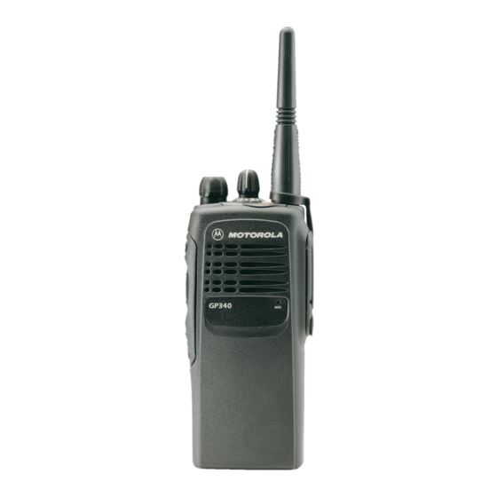
Motorola GP340 Service Information
Gp series
300r1 (300 - 350mhz)
Hide thumbs
Also See for GP340:
- User manual (31 pages) ,
- Basic user's manual (10 pages) ,
- Specification sheet (5 pages)

Related Manuals for Motorola GP340


Summary of Contents for Motorola GP340
- Page 1 Professional Radio GP Series 300R1 (300 - 350MHz) Service Information Issue: December 1999...
-
Page 2: Computer Software Copyrights
Accordingly, any copyrighted Motorola computer programs contained in the Motorola products described in this manual may not be copied or reproduced in any manner without the express written permission of Motorola. Furthermore, the purchase of Motorola... -
Page 3: Table Of Contents
Table of Contents Chapter 1 MODEL CHART AND TECHNICAL SPECIFICATIONS 1.0 GP340 Model Chart .....................1-1 2.0 GP640 / GP680 Model Chart ................1-1 3.0 Technical Specifications ..................1-2 Chapter 2 THEORY OF OPERATION 1.0 Introduction ......................2-1 2.0 Transmitter......................2-1 2.1 Power Amplifier ....................2-1 2.2 Antenna Switch....................2-2... -
Page 5: Model Chart And Technical Specifications
Chapter 1 MODEL CHART AND TECHNICAL SPECIFICATIONS GP340 Model Chart Professional GP300 Series (300-350MHz) Model Description MDH25EDC9AN3_E GP340 300R1 300-350 MHz 4W 16 CH Item Description PMLD4141_ GP340 Back Cover Kit 6864110B13_ GP340 Basic User Guide PMAD4022_ 9cm (300-344 MHz) Antenna... -
Page 6: Technical Specifications
MODEL CHART AND TECHNICAL SPECIFICATIONS Technical Specifications Data is specified for +25°C unless otherwise stated. General Specifications Channel Capacity GP340 GP640 16 (Conventional) GP680 16 (Conventional) Power Supply Rechargeable battery 7.5v Dimensions: H x W x D (mm) Height excluding knobs With standard high capacity NiMH battery 137 x 57.5 x 37.5... - Page 7 Technical Specifications Transmitter 300R1 *Frequencies - Full Bandsplit 300-350 MHz Channel Spacing 12.5/20/25 kHz Frequency Stability ±2.5 ppm @ 12.5kHz (-25°C to +55°C, +25° Ref.) ±5ppm @ 25 kHz Power 1-4W ±2.5 @ 12.5 kHz Modulation Limiting ±4.0 @ 20 kHz ±5.0 @ 25 kHz FM Hum &...
- Page 8 MODEL CHART AND TECHNICAL SPECIFICATIONS...
-
Page 9: Theory Of Operation
Chapter 2 THEORY OF OPERATION Introduction This Chapter provides a detailed theory of operation for the 300-350MHz circuits in the radio. For details of the theory of operation and trouble shooting for the the associated Controller circuits refer to the Controller Section of this manual. Transmitter (Refer to Figure 2-1 and the Transmitter schematic diagram) The transmitter contains five basic circuits:... -
Page 10: Antenna Switch
THEORY OF OPERATION The PRF1507 LDMOS PA is capable of supplying an output power of 7W with an input signal of 0.3W. The current drain would typically be 1300mA while operating in the frequency range of 300-350MHz. The power output can be varied by changing the biasing voltage. Antenna Switch The antenna switch circuit consists of two PIN diodes (CR101 and CR102), a pi network (C107, L104 and C106), and two current limiting resistors (R101, R170). -
Page 11: Receiver
Receiver Receiver Antenna Pin Diode Varactor Varactor Antenna Crystal RF Amp Mixer IF Amp Tuned Filter Tuned Filter Switch RF Jack Filter First LO from FGU Control Voltage from ASFIC Recovered Audio Demodulator Squelch U301 RSSI Synthesizer 16.8 MHz Reference Clock SPI Bus Second LO VCO... -
Page 12: Receiver Back-End
THEORY OF OPERATION Both the pre and post-RF amplifier varactor tuned filters have similar responses. The 3dB bandwidth of the filter is about 50 MHz. This enables the filters to be electronically controlled by using a single control voltage which is DACRx . The output of the post-RF amplifier filter which is connected to the passive double balanced mixer consists of T301, T302 and CR306. -
Page 13: Automatic Gain Control Circuit
Receiver Automatic Gain Control Circuit (Refer to the Receiver Front End and Receiver Back End schematic diagrams) The front end automatic gain control circuit is to provide automatic gain reduction of the front end RF amplifier via feedback. This action is necessary to prevent overloading of backend circuits. This is achieved by drawing some of the output power from the RF amplifier’s output. -
Page 14: Frequency Generation Circuitry
THEORY OF OPERATION Frequency Generation Circuitry (Refer to Figure 2-3 and the Frequency Synthesizer schematic diagram) The Frequency Generation Circuitry is composed of two main ICs, the Fractional-N synthesizer (U201), and the VCO/Buffer IC (U241). Designed in conjunction to maximize compatibility, the two ICs provide many of the functions that normally would require additional circuitry. - Page 15 Frequency Generation Circuitry In achieving fast locking for the synthesizer, an internal adapt charge pump provides higher current at pin 45 of U201 to put synthesizer within the lock range. The required frequency is then locked by normal mode charge pump at pin 43 . Both the normal and adapt charge pumps get their supply from the capacitive voltage multiplier which is made up of C258, C259, C228, triple diode CR201 and level shifters U210 and U211.
-
Page 16: Voltage Controlled Oscillator (Vco)
THEORY OF OPERATION Voltage Controlled Oscillator (VCO) (Refer to Figure 2-5 and the Voltage Controlled Oscillator schematic diagram) The VCOBIC (U241) in conjunction with the Fractional-N synthesizer (U201) generates RF in both the receive and the transmit modes of operation. The TRB line (U241 pin 19) determines which oscillator and buffer will be enabled. - Page 17 Frequency Generation Circuitry Table 2-1 Level Shifter Logic Desired AUX 4 AUX 3 Mode High (@3.2V) High (@4.8V) High Battery Saver Hi-Z/Float (@2.5V) In the receive mode, U241 pin 19 is low or grounded. This activates the receive VCO by enabling the receive oscillator and the receive buffer of U241.
- Page 18 2-10 THEORY OF OPERATION...
-
Page 19: Troubleshooting Charts
Chapter 3 TROUBLESHOOTING CHARTS Troubleshooting Flow Chart for Receiver (Sheet 1 of 2) START Bad SINAD Bad 20dB Quieting No Recovered Audio udio Check Controller at pin 27 of U301? Spray of inject 1st IF into XTAL Filter IF Freq: 45.1MHz Check Q320 bias circuitry for faults. -
Page 20: Troubleshooting Flow Chart For Receiver (Sheet 2 Of 2)
TROUBLESHOOTING CHARTS Troubleshooting Flow Chart for Receiver (Sheet 2 of 2) Inject RF into J101 Q302 Trace IF signal collector OK? IF Signal from L311 to IF signal at L311? Q302. Check for present? bad XTAL filter. Before replacing U301, check U301 voltages;... -
Page 21: Troubleshooting Flow Chart For Transmitter
Troubleshooting Flow Chart for Transmitter Troubleshooting Flow Chart for Transmitter START No Power Is There B+ Bias for Check Q111 Ant switch CR101 Is Current Check PCIC Is Control Voltage High or Low at C119 High 1. Check Pin Diodes Check Drive to 2. -
Page 22: Troubleshooting Flow Chart For Synthesizer
TROUBLESHOOTING CHARTS Troubleshooting Flow Chart for Synthesizer 3.3V at Check U248, Start U201 pins 5, L201 & L202 20, 34& Check CR201, Visual U210, U211, Correct check of the C258, C259 & Problem Board OK? C228 Is U201 16.8MHz 16.8MHz at pin 6 of Pin47 AT = Replace... -
Page 23: Troubleshooting Flow Chart For Vco
Troubleshooting Flow Chart for VCO Troubleshooting Flow Chart for VCO START No LO? U241 Check R245 TRB = Pin 10 for dry joint 5V? @U241 Carrier? >1V? or faulty Pin 19 VCO OK L253 Change Open L253 Circuit? AUX 3 Check High? R260... - Page 24 TROUBLESHOOTING CHARTS...
-
Page 25: Allocation Of Schematics And Circuit Boards
Chapter 4 PCB/SCHEMATICS/PARTS LISTS Allocation of Schematics and Circuit Boards Controller Circuits The 300-350MHz circuits are contained on the printed circuit board (PCB) which also contains the Controller circuits. This Chapter shows the schematics for the 300R1 circuits only, refer to the Controller section for details of the related Controller circuits.The PCB component layouts and the Parts Lists in this Chapter show both the Controller and 300R1 circuit components. - Page 26 PCB/SCHEMATICS/PARTS LISTS...