Table of Contents
Advertisement
Quick Links
Service
Manual
SECTION
1. TECHNICAL SPECIFICATIONS ........................................................................... 1
2. SERVICE MODE .................................................................................................. 2
3. WIRING DIAGRAM ............................................................................................... 9
4. BLOCK DIAGRAM .............................................................................................. 11
5. SCHEMATIC DIAGRAM ..................................................................................... 13
6. PARTS LOCATION (Pattern Side) ..................................................................... 15
7. IC DATA .............................................................................................................. 21
8. EXPLODED VIEW AND PARTS LIST ................................................................ 27
9. ELECTRICAL PARTS LIST ................................................................................ 32
Please use this service manual with referring to the user guide ( D.F.U. ) without fail.
STANDBY
STANDBY
SOURCE
DISPLAY
REC MODE
DUBB.
REC
CHARACTER
EDIT
TABLE OF CONTENTS
MD110
MD110 /
MD Deck
OPEN
MD110
OPEN
MULTI JOG
PUSH ENTER
PAGE
325W855010 MIT
3120 785 22730
First Issue 2001.12
F1S, /N1S
R
Advertisement
Table of Contents

Related Manuals for Marantz MD110


Summary of Contents for Marantz MD110
-
Page 1: Table Of Contents
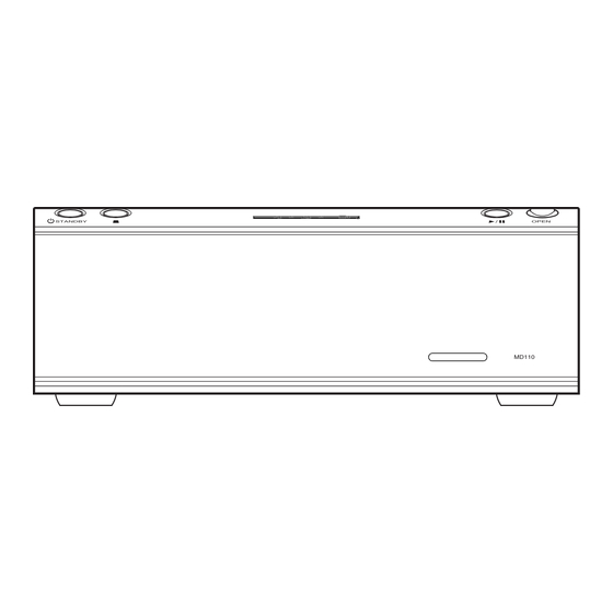
Service MD110 / F1S, /N1S Manual MD Deck STANDBY OPEN MD110 STANDBY OPEN SOURCE DISPLAY REC MODE DUBB. MULTI JOG PUSH ENTER CHARACTER EDIT TABLE OF CONTENTS SECTION PAGE 1. TECHNICAL SPECIFICATIONS ................1 2. SERVICE MODE ....................2 3. WIRING DIAGRAM ....................9 4. - Page 2 MARANTZ Parts for your equipment are generally available to our National Marantz Subsidiary or Agent. ORDERING PARTS : Parts can be ordered either by mail or by Fax.. In both cases, the correct part number has to be specified.
-
Page 3: Technical Specifications
1. TECHNICAL SPECIFICATIONS MAIN UNIT (MD110) Type ........................... MiniDisc Digital Audio System Laser ............................Semiconductor laser Recording method ................Magnetic field modulation overwrite method RPMs ......................Approximately 400rpm to 900rpm (CLV) Sampling frequency ............................. 44.1 kHz Frequency characteristics ......................20 to 20 kHz (± 1 dB) S/N .............................. -
Page 4: Service Mode
2. SERVICE MODE Service Mode 1. While Mains cord is disconnected, press DISPLAY Button on the unit and plug in the Mains cord. 2. Version number of the front micom software is displayed. 3. Turn JOG dial to either direction then Display segment test begins. 4. - Page 5 TEST MODE 1 How to Setting and Cancel Test Mode Setting: While pressing the PLAY/PAUSE keys, insert the power cord to the wall outlet. Cancel: Pull out the power cord. Key Operation for Adjustment Operation MULTI JOG Select parameter and mode. PLAY Fix items.
- Page 6 2. Change of Playback Points (In continuous playback mode) Display/Function PL AY [CPLAY OUT] Carry out No.4 and 5 in the above table PL AY [CPLAY IN] Carry out No.4 and 5 in the above table ST OP [CPLAY MODE] EJECT Disc out 5 Continuous Recording Mode 1.
- Page 7 2 Precaution on handling of Optical pick-up (KMS-260B) The laser diode in an optical pick-up is easy to be subject to electrostatic destruction. Therefore, solder-bridge the laser tap on the flexible board when handling the optical pick-up. When removing the flexible board from the connector, make a solder bridge in advance, then remove the board. Be careful not to remove the solder bridge before inserting the connector.
- Page 8 6 Laser Power Check and Adjustment Laser power setting in playback and recording modes. Preparation 1. Remove the MD mechanism from the unit 2. Remove the case and bracket. 3. Reconnect the flat cable of MD mechanism to the unit 1.
- Page 9 FE Balance 1. Recordable Disc Display/Function Connect the oscilloscope to TE1 and VC in X33 PCB MULTI JOG Select [EFBAL ADJUST] Load the recordable disc PL AY [EFBAL MO-W] PL AY [EF=$**MOW] MULTI JOG Write adjustment. Adjust the waveform as follows. PLAY Display shows [EF=$**MOR] after [EFB=**xSAVE] to save the data in E2PROM.
- Page 10 8 Focus Bias Adjustment Use the special disc (continuous recorded disc) Display/Function MULTI JOG Select [FBIAS ADJUST] Load the disc. PLAY [a=xx yyyy/zz] point a (xx = focus bias yyyy = C1error) Adjust "yyyy" to 220* PLAY [b=xx yyyy/zz] point b DOWN Adjust "yyyy"...
-
Page 11: Wiring Diagram
3. WIRING DIAGRAM... -
Page 12: Block Diagram
4. BLOCK DIAGRAM... -
Page 13: Schematic Diagram
5. SCHEMATIC DIAGRAM... -
Page 14: Parts Location (Pattern Side)
6. PARTS LOCATION (Pattern Side) MAIN BOARD IC12 IC10 IC11 REC BOARD... - Page 15 MAIN BOARD Q4L Q4R Q16-Q18 Q1 Q2 IC4 Q3L Q3R Q5-Q7 IC13 Q14 Q15 REC BOARD...
- Page 16 FRONT BOARD Q300 Q301 Q302 Q307 Q303 - Q306...
-
Page 17: Ic Data
7. IC DATA IC1/3/4:NJM2068 Pin Configuration IC7:TL431 Pin Assignment LP PACKAGE (TOP VIEW) CATHODE ANODE Functional Block Diagram CATHODE V ref ANODE... - Page 18 IC2:KIC9459N PIN CONNECTION PIN DESCRIPTION...
- Page 19 IC300:M66005F PIN CONFIGURATION PIN DESCRIPTIONS Symbol Comment Pin name Reset input When "L", M66005 is initialized. RESET When "L", communication with the MCU is possible. Chip select input When "H", any instruction from the MCU is neglected. Shift clock input Serial input data is taken and shifted by the positive edge of SCK.
- Page 20 IC13:74HC04 PIN DESCRIPTION PIN NO. SYMBOL NAME AND FUNCTION 1, 3, 5, 9, 11, 13 1A to 6A data inputs 2, 4, 6, 8, 10, 12 1Y to 6Y data outputs ground (0 V) positive supply voltage Fig.5 Schematic diagram Fig.1 Pin configuration.
- Page 21 IC6:CXP84648 PIN NO PIN NAME OPERATION DESCRIPTION ASSIGN PIN ASSIGNMENT A_MUTE OUTPUT A_MUTE ACTIVE LOW D_MUTE OUTPUT D_MUTE ACTIVE LOW PO_OFF_CONT OUTPUT FOR RLY ACTIVE HIGH BACKUP_V RESET INPUT CPU ACTIVE HIGH EXTAL OUTPUT FOR 12.288MHZ CRYSTAL XTAL 12.288MHZ CRYSTAL 32MHZ CRYSTAL OUTPUT FOR 32MHZ CRYSTAL AVSS...
-
Page 22: Exploded View And Parts List
8. EXPLODED VIEW AND PARTS LIST A X2 E X2 E X2 C X7 L X4 K X7 K X2 D X4 8 X3 M X2 F X2 39 X2 7 X3 A X4 22 X4 6 X3 21 X3 38 X2 K X2 4 X2... - Page 23 9965 000 11113 CABINET TOP 324W257010 CARD PLATE EARTH "C" CARD PLATE EARTH "F" CARD PLATE EARTH "D" BOX,GIFT 325W801010 TAPE ARM CUSHION,SNOW 323W809010 TAPE LENS NOTE : "nsp" PART IS LISTED FOR REFERENCE ONLY, MARANTZ WILL NOT SUPPLY THESE PARTS.
- Page 25 MACHINE SCREW(B) 1.7*4.5 T42-0983 MOTOR ASSY *MM001170R E35-2689 WIRING HARNESS(SLED) E35-2690 WIRE HARNESS E35-2691 FLAT CABLE L=80MM *YU000960R E35-2348 FLAT CABLE(PU) 21P *YU000970R X33-1260 PCB ASSY *ZZ001870R NOTE : "nsp" PART IS LISTED FOR REFERENCE ONLY, MARANTZ WILL NOT SUPPLY THESE PARTS.
-
Page 26: Electrical Parts List
9. ELECTRICAL PARTS LIST NOTE ON SAFETY FOR FUSIBLE RESISTOR : ASSIGNMENT OF COMMON PARTS CODES. RESISTORS The suppliers and their type numbers of fusible resistors : 1) GD05 × × × 140, Carbon film fixed resistor, ±5% 1/4W are as follows; : 2) GD05 ×... - Page 27 9965 000 11128 DOUBLE LAYER(70), *EX000090R CHIP,10K-J,1/16W-1608REEL 0.047F-70UA/5.5V-5RE R71L CHIP,680-J,1/16W-1608REEL ELECT,47µF-M/16V,5x11-5RE R71R CHIP,680-J,1/16W-1608REEL CER.CHIP,0.1µF-K/50V-1608 1-J,1/4W-R.TYPE REEL CER.CHIP,18pF-J/50V-1608 CHIP,47K-J,1/16W-1608REEL CER.CHIP,18pF-J/50V-1608 CHIP,2.2K-J,1/16W-1608REEL 1-J,1/4W-R.TYPE REEL MAIN - RESISTORS CHIP,3.3K-J,1/16W-1608REEL CHIP,3.3K-J,1/16W-1608REEL NOTE : "nsp" PART IS LISTED FOR REFERENCE ONLY, MARANTZ WILL NOT SUPPLY THESE PARTS.
- Page 28 9965 000 11423 CRYSTAL,12.288MHZ, *JX000890R 4822 130 60729 CHIP TRS.2SC, *BA001040R HC49U-CL;20pF DTC144EK,0.2W/SMT-REEL XTAL2 9965 000 11124 CRYSTAL,MX-38T(32.768KHZ) *JX000830R 9965 000 10753 CHIP TRS.2SC, *BA001220R KRC102S T/P (KEC) NOTE : "nsp" PART IS LISTED FOR REFERENCE ONLY, MARANTZ WILL NOT SUPPLY THESE PARTS.
- Page 29 4822 130 60941 CHIP TRS.2SA,DTA114EK, BA10023210 CHIP,100-J,1/16W-1608REEL 0.2W/SMT-REEL CHIP,1.5K-J,1/16W-1608REEL Q306 9965 000 11131 CHIP TRS.2SC,KRC104S (SOP) *BA001290R CHIP,1.5K-J,1/16W-1608REEL Q307 9965 000 10753 CHIP TRS.2SC,KRC102S T/P *BA001220R (KEC) NOTE : "nsp" PART IS LISTED FOR REFERENCE ONLY, MARANTZ WILL NOT SUPPLY THESE PARTS.
- Page 30 5322 209 13406 IC,NJM2068MD-SOP8P *HC107380R REC - MISCELLANEOUS BKT1 BRACKET,AVR3300(E3) (DENON) SPTE 0.8t/SCREW BKT2 BRACKET,AVR3300(E3) (DENON) SPTE 0.8t/SCREW CN.WAFER 2.0MM, 35237-1010 10P CN.WAFER 2.0MM, 35237-0510 5P CHIP,0-J,1/8W-3216REEL J109 NOTE : "nsp" PART IS LISTED FOR REFERENCE ONLY, MARANTZ WILL NOT SUPPLY THESE PARTS.