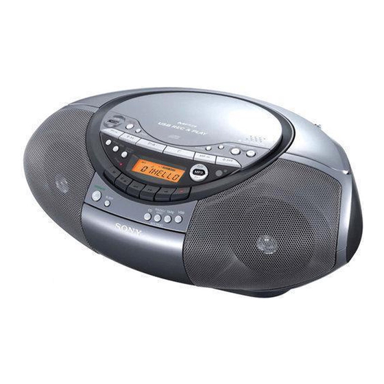
Sony CFD-RS60CP Service Manual
Hide thumbs
Also See for CFD-RS60CP:
- Operating instructions (2 pages) ,
- Operating instructions (2 pages)
Table of Contents
Advertisement
Quick Links
SERVICE MANUAL
Ver. 1.0 2007.07
CD player section
System
Compact disc digital audio system
Laser diode properties
Emission duration: Continuous
Laser output: Less than 44.6 µW
(This output is the value measured at a distance of
about 200 mm from the objective lens surface on the
optical pick-up block with 7 mm aperture.)
Spindle speed
200 r/min (rpm) to 500 r/min (rpm) (CLV)
Number of channels
2
Frequency response
20 - 20 000 Hz +1.8/–0.2 dB
Wow and flutter
Below measurable limit
Radio section
Frequency range
MX model
FM: 87.5 - 108 MHz
AM: 530 - 1 710 kHz
E41, SP model
FM: 87.5 - 108 MHz
AM: 531 - 1 611 kHz (9 kHz step)
530 - 1 610 kHz (10 kHz step)
Sony Corporation
9-887-803-01
Personal Audio Division
2007G04-1
Published by Sony Techno Create Corporation
© 2007.07
CFD-RS60CP
Model Name Using Similar Mechanism CFD-S35CP
CD
CD Mechanism Type
Section
Optical Pick-up Name
Model Name Using Similar Mechanism NEW
TC
Section Tape Transport Mechanism Type
SPECIFICATIONS
Antennas
FM: Telescopic antenna
AM: Built-in ferrite bar antenna
Cassette-corder section
Recording system
4-track 2 channel stereo
Fast winding time
Approx. 120 s (sec.) with Sony cassette C-60
Frequency response
TYPE I (normal): 80 - 10 000 Hz
USB section
Supported bit rate
MP3 (MPEG 1 Audio Layer-3):
32 - 320 kbps, VBR
Sampling frequencies
MP3 (MPEG 1 Audio Layer-3):
32/44.1/48 kHz
(USB) port
USB-A (Full Speed)
CD RADIO CASSETTE-CORDER
E Model
KSM-213CDP
KSS-213C
MF-S350V
– Continued on next page –
Advertisement
Table of Contents

Related Manuals for Sony CFD-RS60CP


Summary of Contents for Sony CFD-RS60CP
- Page 1 200 mm from the objective lens surface on the Fast winding time optical pick-up block with 7 mm aperture.) Approx. 120 s (sec.) with Sony cassette C-60 Spindle speed Frequency response 200 r/min (rpm) to 500 r/min (rpm) (CLV)
- Page 2 COMPONENTS IDENTIFIED BY MARK 0 OR DOTTED LINE WITH MARK 0 ON THE SCHEMATIC DIAGRAMS AND IN THE PARTS LIST ARE CRITICAL TO SAFE OPERATION. REPLACE THESE COMPONENTS WITH SONY PARTS WHOSE PART NUMBERS APPEAR AS SHOWN IN THIS MANUAL OR IN SUPPLEMENTS PUBLISHED BY SONY.
-
Page 3: Table Of Contents
CFD-RS60CP UNLEADED SOLDER TABLE OF CONTENTS Boards requiring use of unleaded solder are printed with the lead- free mark (LF) indicating the solder contains no lead. SERVICING NOTES ..........4 (Caution: Some printed circuit boards may not come printed with... -
Page 4: Servicing Notes
CFD-RS60CP SECTION 1 SERVICING NOTES LASER DIODE AND FOCUS SEARCH OPERATION CHUCK PLATE JIG ON REPAIRING CHECK 1. Turn ON the [OPERATE] button and press [CD] button to CD On repairing CD section, playing a disc without the lid (CD), use position. -
Page 5: General
CFD-RS60CP SECTION 2 GENERAL This section is extracted from instruction manual. Basic Operations Basic Operations Audio CD To adjust the volume Listening to the radio Press VOLUME +, – (VOL +, – on the remote) 9. Press RADIO qs on the unit (BAND wa on the To listen through headphones remote) repeatedly. -
Page 6: Disassembly
CFD-RS60CP SECTION 3 DISASSEMBLY Note: Disassemble the unit in the order as shown below. 3-1. CABINET TOP ASSY (Page 7) 3-2. CABINET FRONT ASSY, 3-9. CD LID 3-10. LCD BLOCK ASSY, CABINET BOTTOM ASSY (Page 11) USB CONNECT BOARD (Page 7) (Page 11) 3-11. -
Page 7: Cabinet Top Assy
CFD-RS60CP Note: Follow the disassembly procedure in the numerical order given. 3-1. CABINET TOP ASSY 5 two screws 7 three screws (+BV tapping (B2.6 ) ) (+BV tapping (B2.6 ) ) 4 CD lid 8 two screws (+BV tapping (B2.6 ) ) -
Page 8: Wires
CFD-RS60CP 3-3. WIRES Put flat cable and wires between the cabinets and push them in the grooves located at A to G in the figure to prevent disconnection from HEADPHONE board before assembling the set. cabinet front cabinet bottom 3-4. MD BLOCK 1 two screws (+P tapping (B2.6 ) ) -
Page 9: Holder (Cassette)
CFD-RS60CP 3-5. HOLDER (CASSETTE) 1 screw (+BV tapping (B2.6 ) ) 2 damper two claws 4 spring (cassette) two claws 3 holder (cassette) 3-6. POWER KEY BOARD 3 holder (function) 1 two screws 4 three screws 8 button (power) 2 screw... -
Page 10: Main Board Section, Headphone Board
CFD-RS60CP 3-7. MAIN BOARD SECTION, HEADPHONE BOARD 5 two screws 2 two screws (+P tapping (B2.6 ) ) (+BV tapping (B2.6 ) ) 6 VOL board 4 CN351 (10P) clamp 9 two screws (+P tapping (B2.6 ) ) 3 HEADPHONE board... -
Page 11: Cd Lid
CFD-RS60CP 3-9. CD LID 3 CD lid 2 two claws 1 two claws spring (CD) 3-10. LCD BLOCK ASSY, USB CONNECT BOARD qj USB CONNECTOR board qk bracket (USB connector) 0 CN402 (5core) qs button (mode) qa screw qh two screws (+BV tapping (B2.6 ) ) -
Page 12: Cd Block Assy
CFD-RS60CP 3-11. CD BLOCK ASSY two claws 3 CD cover two claws 4 CD block assy 1 two screws 2 two screws (+PWH tapping (B2.6 ) ) (+PWH tapping (B2.6 ) ) 3-12. R/P HEAD (HRP301), ERASE HEAD (HE301), TC BOARD 5 Remove the four solderings. -
Page 13: Mechanical Adjustments
CFD-RS60CP SECTION 4 SECTION 5 MECHANICAL ADJUSTMENTS ELECTRICAL ADJUSTMENTS • Precaution TAPE SECTION 0 dB = 0.775 V 1. Clean the following parts with a denatured alcohol-moistened swab : • Standard Output Level record/playback heads pinch roller Output terminal HP OUT... -
Page 14: Tuner Section
CFD-RS60CP TUNER SECTION 0 dB = 1 µV AM IF ADJUSTMENT Adjust for a maximum reading on level meter 450 kHz [AM] Setting: AM FREQUENCY COVERAGE ADJUSTMENT (MX model) Function: RADIO Adjustment Part Frequency Display Reading on Digital Voltmeter Band: AM 530 kHz 1.0 ±... - Page 15 CFD-RS60CP Adjustment and Connecting Location: AM TRACKING ADJUSTMENT – TUNER BOARD (Component Side) – FM FREQUENCY COVERAGE ADJUSTMENT TP-ANT (JW2) FM TRACKNG ADJUSTMENT AM IF ADJUSTMENT AM TRACKING ADJUSTMENT FM IF ADJUSTMENT FM FREQUENCY AM FREQUENCY COVERAGE COVERAGE ADJUSTMENT ADJUSTMENT –...
-
Page 16: Cd Section
CFD-RS60CP [RF LEVEL CHECK] CD SECTION oscilloscope [TEST DISC LIST] Use the following test disc on test mode. BD91 board • CD: YEDS-18 (PART No. 3-702-101-01) TP123 (RFO) TP124 (VC) – PATD-012 (PART No. 4-225-203-01) Note: Procedure : 1. CD Block is basically designed to operate without adjustment. -
Page 17: Diagrams
CFD-RS60CP SECTION 6 DIAGRAMS 6-1. BLOCK DIAGRAM – CD Section – CD+1.5V CD+1.5V REG VDD1 DVDD+3.3V IC201 FNI1 CD LCH MAIN FPI1 SECTION CD RCH FNI2 (Page 20) DETECTOR FPI2 • Signal Path DATA AOUT2(PO5) BCK(PO8) : CD PLAY PIO3... -
Page 18: Block Diagram - Tuner Section
CFD-RS60CP 6-2. BLOCK DIAGRAM – TUNER Section – FM IFT FM/AM FRONT-END, FM IF IF AMP, DET, MPX ANT1 FM TELESCOPIC ANTENNA L-OUT IF-IN RF-IN MIX-OUT FM IF TU-L -OUT MAIN RF AMP MUTE SECTION BUFFER R-OUT TU-R (Page 20) -
Page 19: Block Diagram - Usb Section
CFD-RS60CP 6-3. BLOCK DIAGRAM – USB Section – USB CONTROL S-RAM IC901 IC921 VBUS POWER ON/OFF SWITCH (VBUS) I/O0 IC915 I/O3 • I/O4 P00/D0 D0 – 15 I/O7 P75/USBOC P07/D7 • • EN 1 P76/USBPON I/O8 P10/D8 I/O11 P17/D15 •... -
Page 20: Block Diagram - Main Section
CFD-RS60CP 6-4. BLOCK DIAGRAM – MAIN Section – TU-R TUNER SECTION TU-L (Page 18) IC351 R.RO ELECTRONIC VOLUME R.IN R.LINE REC/PB POWER AMP CD-R R-CH R.RAD PRE AMP IC301 IC301 L.RO VOL AMP J371 SECTION ALC 2 L-IN1 L-OUT L.LINE L.LO... - Page 21 CFD-RS60CP • NOTE FOR PRINTED WIRING BOARDS AND SCHEMATIC DIAGRAMS • Circuit Boards Location THIS NOTE IS COMMON FOR PRINTED WIRING BOARDS AND SCHEMATIC DIAGRAMS. (In addition to this, the necessary note is printed in each block.) Note on Schematic Diagrams: Note on Printed Wiring Boards: •...
-
Page 22: Printed Wiring Board - Bd91 Section
CFD-RS60CP 6-5. PRINTED WIRING BOARD – BD91 Section – • See page 21 for Circuit Boards Location. : Uses unleaded solder. M401 (SPINDLE) S201 (LIMIT) C404 C403 R402 M402 (SLED) C122 R140 C123 IC401 R143 R118 C138 R128 C153 C137... -
Page 23: Schematic Diagram - Bd91 Section
CFD-RS60CP • See page 39 for Waveforms. • See page 40 for IC Block Diagrams. 6-6. SCHEMATIC DIAGRAM – BD91 Section – • See page 43 for IC Pin Description of IC101. C107 C136 C112 R108 R129 R139 R128 CN202... -
Page 24: Printed Wiring Board - Tuner Section
CFD-RS60CP 6-7. PRINTED WIRING BOARD – TUNER Section – • See page 21 for Circuit Boards Location. : Uses unleaded solder. MX MODEL E41,SP MODEL (CV) MAIN BOARD CN804 (Page 26) MX MODEL (GND) E41,SP MODEL 1-863-438- • Semiconductor Location Ref. -
Page 25: Schematic Diagram - Tuner Section
CFD-RS60CP • See page 41 for IC Block Diagrams. 6-8. SCHEMATIC DIAGRAM – TUNER Section – • See page 39 for Waveform. IC B/D JC12 JC11 LC72137M-TLM-E MODEL E41,SP MODEL JC24 MX MODEL CNP1 ANT1 IC B/D MAIN BOARD (1/2) -
Page 26: Printed Wiring Board - Main Section
CFD-RS60CP 6-9. PRINTED WIRING BOARD – MAIN Section – • See page 21 for Circuit Boards Location. : Uses unleaded solder. MAIN BOARD (Page 36) (Page 37) POWER KEY BOARD BOARD BOARD S801 CN407 CN403 CN303 PUSH (Page 34) C110... -
Page 27: Schematic Diagram - Main Section (1/2)
CFD-RS60CP • See page 39 for Waveform. 6-10. SCHEMATIC DIAGRAM – MAIN Section (1/2) – • See page 46 for IC Pin Description of IC801. Q807 TP821 CN804 C895 Q808 Q809 R110 TP824 C854 C847 TP822 C897 R210 C896 (Page 25) -
Page 28: Schematic Diagram - Main Section (2/2)
CFD-RS60CP 6-11. SCHEMATIC DIAGRAM – MAIN Section (2/2) – IC301 C108 Q101 R106 C101 C102 CN301 TP302 R112 R105 R303 R107 C304 TP303 C203 C103 C201 (Page 31) R302 R207 C204 C104 CN302 R212 R205 R201 R101 R206 Q201 C208... -
Page 29: Printed Wiring Boards - Power Section
CFD-RS60CP 6-12. PRINTED WIRING BOARDS – POWER Section – • See page 21 for Circuit Boards Location. : Uses unleaded solder. BATTERY (2) BOARD BATTERY (1) BOARD POWER BOARD T951 JW952 – JW953 DRY BATTERY SIZE “D” (IEC DESIGNATION R20) -
Page 30: Printed Wiring Boards - Headphone/Usb Connect/Vol Section
CFD-RS60CP 6-13. PRINTED WIRING BOARDS – HEADPHONE/USB CONNECT/VOL Section – • See page 21 for Circuit Boards Location. : Uses unleaded solder. J371 USB CONNECT HEADPHONE J1001 BOARD BOARD VOL BOARD L351 MAIN BOARD CN302 L352 (Page 26) R271 C353... -
Page 31: Schematic Diagram - Headphone/Usb Connect/Vol Section
CFD-RS60CP 6-14. SCHEMATIC DIAGRAM – HEADPHONE/USB CONNECT/VOL Section – IC351 C254 C255 L351 CN351 C253 JC351 (Page 28) R251 C252 R151 C152 R354 L352 C153 C354 C355 R353 R356 C154 R355 C353 TP351 C155 C352 R352 R351 C351 (Page 27) -
Page 32: Printed Wiring Board - Usb Section
CFD-RS60CP 6-15. PRINTED WIRING BOARD – USB Section – • See page 21 for Circuit Boards Location. : Uses unleaded solder. C902 C903 C904 CN904 R928 R921 IC915 C901 C914 R945 R938 R983 RB921 C916 R937 R933 C907 RB922 IC901... -
Page 33: Schematic Diagram - Usb Section
CFD-RS60CP • See page 39 for Waveform. • See page 42 for IC Block Diagram. 6-16. SCHEMATIC DIAGRAM – USB Section – • See page 48 for IC Pin Description of IC901. CN901 TP914 MAIN BOARD (2/2) CN803 TP913 (Page 28) -
Page 34: Printed Wiring Board - Tc Section
CFD-RS60CP 6-17. PRINTED WIRING BOARD – TC Section – • See page 21 for Circuit Boards Location. : Uses unleaded solder. C308 T301 C307 C310 C305 R307 R308 C304 R306 C306 CN303 IC301 JC304 R302 R202 R206 R303 S301 MAIN... -
Page 35: Schematic Diagram - Tc Section
CFD-RS60CP • See page 39 for Waveforms. 6-18. SCHEMATIC DIAGRAM – TC Section – • See page 42 for IC Block Diagrams. IC301 TA2068NG IC B/D R103 R112 R301 C102 R102 R111 C103 R104 C301 C104 C101 <<0>> C107 JC302... -
Page 36: Printed Wiring Boards - Key Section
CFD-RS60CP 6-19. PRINTED WIRING BOARDS – KEY Section – • See page 21 for Circuit Boards Location. : Uses unleaded solder. CD KEY BOARD (Page 37) BOARD CN402 S410 VOLUME S411 S409 S401 S412 S402 VOLUME ERASE CD-USB MEGABASS SOUND –... -
Page 37: Printed Wiring Board - Lcd Section
CFD-RS60CP 6-20. PRINTED WIRING BOARD – LCD Section – • See page 21 for Circuit Boards Location. : Uses unleaded solder. (Page 26) (Page 36) MAIN CD KEY BOARD BOARD CN408 CN401 LCD BOARD C408 CN407 R465 L401 S421 S421... -
Page 38: Schematic Diagram - Control Section
CFD-RS60CP 6-21. SCHEMATIC DIAGRAM – CONTROL Section – • See page 39 for Waveform. R449 LCD401 R436 R450 R435 R451 R452 R434 R453 R433 R454 R432 R455 R431 IC402 R456 R430 R457 R429 R428 R427 R426 R425 R475 R474 R473... - Page 39 CFD-RS60CP • Waveforms – TUNER Board – – TC Board – – BD91 Board – (CD PLAY) IC101 5 (FEI) IC2 w; (XOUT) Q301 C REC 4 Vp-p Approx. 1.0 Vp-p 200 mVp-p 19.5 µ sec 75 kHz 0.5 V/DIV, 5 µ sec/DIV 100 mV/DIV, 5 msec/DIV 0.1 V/DIV, 5 µ...
-
Page 40: Ic Block Diagrams
CFD-RS60CP • IC Block Diagrams IC201 TK63115SCL-G@GT (BD91 Board) VIN 1 VOUT GND 2 V REF ON/OFF THERMAL & CONTROL OVER CURRENT PROTECTION VCONT 4 NC IC401 BA5826SFP-E2 (BD91 Board) VO1(-) VOL(-) VO1(+) LEVEL VOL(+) SHIFT LEVEL 13.3K SHIFT T.S.D. - Page 41 CFD-RS60CP IC1 TA2149BN (TUNER Board) GND1 FM RF-OUT FM RF VCC1 FM RF-IN AM RF-IN AM LOW CUT MIX-OUT FM OSC AM OSC BUFF BUFF 1/1 OR VCC2 OSC-OUT LEVEL 1/16 AM IF AF IF-IN ST-IND IF BUFF FM IF...
- Page 42 CFD-RS60CP IC915 R5523N001B-TR-F (USB Board) 5 OUT GATE CURRENT CONTROL LIMIT 4 IN UVLO FLAG DELAY THERMAL SHUTDOWN IC301 TA2068NG (TC Board) LINE L.LIN L.PO MIC I/EX AMP1 BUF AMP TAPE L.NF RADIO L.RAD AMP1 L.RO MONITOR 26dB BUF AMP MUTE L.IN...
- Page 43 CFD-RS60CP • IC Pin Descriptions IC101 TC94A70FG-008 (S, D) (RF AMP, FOCUS/TRACKING ERROR AMP, DIGITAL SIGNAL PROCESSOR, DIGITAL SERVO PROCESSOR, DIGITAL FILTER, D/A CONVERTER) (BD91 BOARD) Pin No. Pin Name Pin Description AVSS3 — Ground RFZi RF ripple zero crossing signal input...
- Page 44 CFD-RS60CP Pin No. Pin Name Pin Description AoUT3 (PO4) Request signal output to the USB controller Not used. (Open) AoUT2 (PO5) Audio data output to the USB controller PIO0 Request signal output to the system controller or USB controller PIO1...
- Page 45 CFD-RS60CP Pin No. Pin Name Pin Description Light amount monitor input from the laser diode of optical pick-up block RVSS3 — Ground FNi2 (C) Main beam (C) input from the optical pick-up block FNi1 (A) Main beam (A) input from the optical pick-up block...
- Page 46 CFD-RS60CP IC801 MB90F045PF-G-9055-SPE1 (SYSTEM CONTROL) (MAIN BOARD (1/2)) Pin No. Pin Name Pin Description I-SIMUKE1 Destination setting pin I-SIMUKE2 Destination setting pin I-SIMUKE3 Destination setting pin 4 to 6 — Not used. (Open) Z-BUS0 Serial bus data bit 0 input/output...
- Page 47 CFD-RS60CP Pin No. Pin Name Pin Description — Not used. (Open) I-LID-OPEN CD door detect signal input I-AC-CHK AC IN power supply check signal input — Not used. (Open) — Not used. (Open) I-Z-SBSY CD sub code sync signal input...
- Page 48 CFD-RS60CP IC901 TMP92CD28AFG-2CB4 (USB CONTROLLER) (USB BOARD) Pin No. Pin Name Pin Description RESET Reset signal input from the system controller “L”: reset PC0/INT0 Ready to send signal input from the system controller PC1/INT1 Not used. Connected to ground. PC2/INT2/TB1IN0 Not used.
- Page 49 CFD-RS60CP Pin No. Pin Name Pin Description P77/X1USB Not used. (Open) DVSS — Ground PF0/TXD0 Clear to send signal output to the system controller PF1/RXD0 Serial data signal output PF2/SCLK0/CTS0/ Serial data transfer clock signal output CLK/TB0OUT0 PF3/TXD1/SPDO Serial data signal output to the system controller...
-
Page 50: Exploded Views
CFD-RS60CP SECTION 7 EXPLODED VIEWS NOTE: The components identified by mark • Items marked “*” are not stocked since they • Color Indication of Appearance Parts 0 or dotted line with mark 0 are are seldom required for routine service. -
Page 51: Cabinet (Front) Section
CFD-RS60CP 7-2. CABINET (FRONT) SECTION SP301 tape mechanism section not supplied SP302 Ref. No. Part No. Description Remark Ref. No. Part No. Description Remark X-2179-687-1 CABINET (FRONT) SUB ASSY 3-216-207-01 BUTTON (PAUSE) 3-040-916-01 FOOT (FRONT), RUBBER 3-216-208-01 BUTTON (S/E) 3-216-199-01 HOLDER (CASSETTE) -
Page 52: Cabinet (Top) (1) Section
CFD-RS60CP 7-3. CABINET (TOP) (1) SECTION S801 cabinet (top) (2) section S201 Ref. No. Part No. Description Remark Ref. No. Part No. Description Remark 3-923-736-01 COVER, CD 1-452-899-11 MAGNET 3-931-379-21 RUBBER, VIBRATION PROOF (RED) 3-216-198-01 LID, CD 3-252-828-01 SCREW (B2.6), (+) PWH TAPPING... -
Page 53: Cabinet (Top) (2) Section
CFD-RS60CP 7-4. CABINET (TOP) (2) SECTION not supplied not supplied supplied LCD401 not supplied Ref. No. Part No. Description Remark Ref. No. Part No. Description Remark A-1317-472-A BUTTON (CD) ASSY A-1317-475-A USB CONNECT BOARD, COMPLETE 3-254-151-01 SCREW (B2.6), (+) P TAPPING... -
Page 54: Cabinet (Bottom) Section
CFD-RS60CP 7-5. CABINET (BOTTOM) SECTION not supplied not supplied not supplied T951 not supplied (BATTERY (2) board) not supplied not supplied (BATTERY (1) board) F951 not supplied J951 Ref. No. Part No. Description Remark Ref. No. Part No. Description Remark... -
Page 55: Tape Mechanism Section (Mf-S350V)
CFD-RS60CP 7-6. TAPE MECHANISM SECTION (MF-S350V) C309 HRP301 HE301 Ref. No. Part No. Description Remark Ref. No. Part No. Description Remark 3-237-718-01 LEVER, REC 3-252-614-01 CHASSIS, TC 3-254-022-01 SCREW A-1211-775-A MF-S350V//C 1-832-833-21 CABLE, FLEXIBLE FLAT (13 CORE) C309 1-162-923-11 CERAMIC CHIP... -
Page 56: Electrical Parts List
CFD-RS60CP SECTION 8 BATTERY (1) BATTERY (2) ELECTRICAL PARTS LIST BD91 NOTE: The components identified by mark • Due to standardization, replacements in the • Items marked “*” are not stocked since they 0 or dotted line with mark 0 are parts list may be different from the parts are seldom required for routine service. - Page 57 CFD-RS60CP BD91 CD KEY Ref. No. Part No. Description Remark Ref. No. Part No. Description Remark IC401 6-710-637-01 IC BA5826SFP-E2 R216 1-216-809-11 METAL CHIP 1/10W R218 1-216-845-11 METAL CHIP 100K 1/10W < TRANSISTOR > R219 1-216-845-11 METAL CHIP 100K 1/10W...
- Page 58 CFD-RS60CP CD KEY HEADPHONE Ref. No. Part No. Description Remark Ref. No. Part No. Description Remark S405 1-786-726-11 SWITCH, TACTILE (PRESET –/.) < RESISTOR > S406 1-786-726-11 SWITCH, TACTILE (PRESET +/>) S407 1-786-726-11 SWITCH, TACTILE (u) R425 1-216-833-11 METAL CHIP...
- Page 59 CFD-RS60CP MAIN Ref. No. Part No. Description Remark Ref. No. Part No. Description Remark S421 1-786-726-11 SWITCH, TACTILE (REPEAT) C818 1-164-315-11 CERAMIC CHIP 470PF S422 1-786-726-11 SWITCH, TACTILE (MP3 –) C819 1-164-315-11 CERAMIC CHIP 470PF S423 1-786-726-11 SWITCH, TACTILE (MP3...
- Page 60 CFD-RS60CP MAIN Ref. No. Part No. Description Remark Ref. No. Part No. Description Remark C888 1-125-972-11 ELECT 100uF FB806 1-414-445-11 FERRITE, EMI (SMD) (1608) C889 1-162-970-11 CERAMIC CHIP 0.01uF FB807 1-414-445-11 FERRITE, EMI (SMD) (1608) C890 1-125-972-11 ELECT 100uF FB808...
- Page 61 CFD-RS60CP MAIN Ref. No. Part No. Description Remark Ref. No. Part No. Description Remark < RESISTOR > R810 1-216-821-11 METAL CHIP 1/10W R811 1-216-809-11 METAL CHIP 1/10W R101 1-216-789-11 METAL CHIP 1/10W R812 1-216-809-11 METAL CHIP 1/10W R102 1-216-813-11 METAL CHIP...
- Page 62 CFD-RS60CP MAIN POWER POWER KEY Ref. No. Part No. Description Remark Ref. No. Part No. Description Remark R869 1-216-821-11 METAL CHIP 1/10W < VIBRATOR > R870 1-216-821-11 METAL CHIP 1/10W R871 1-216-821-11 METAL CHIP 1/10W X801 1-813-940-21 PIEZOELECTRIC OSCILLATOR (5.53MHz)
- Page 63 CFD-RS60CP TUNER Ref. No. Part No. Description Remark Ref. No. Part No. Description Remark C107 1-162-962-11 CERAMIC CHIP 470PF R212 1-216-827-11 METAL CHIP 3.3K 1/10W C201 1-162-964-11 CERAMIC CHIP 0.001uF R301 1-216-857-11 METAL CHIP 1/10W C202 1-104-658-11 ELECT 100uF R302 1-216-829-11 METAL CHIP 4.7K...
- Page 64 CFD-RS60CP TUNER Ref. No. Part No. Description Remark Ref. No. Part No. Description Remark 1-162-970-11 CERAMIC CHIP 0.01uF 1-216-864-11 SHORT CHIP 1-162-970-11 CERAMIC CHIP 0.01uF 1-216-864-11 SHORT CHIP 1-162-970-11 CERAMIC CHIP 0.01uF 1-216-864-11 SHORT CHIP 1-162-970-11 CERAMIC CHIP 0.01uF JC11...
- Page 65 CFD-RS60CP TUNER Ref. No. Part No. Description Remark Ref. No. Part No. Description Remark < VIBRATOR > R903 1-216-829-11 METAL CHIP 4.7K 1/10W R904 1-216-829-11 METAL CHIP 4.7K 1/10W 1-795-449-11 VIBRATOR, CRYSTAL (75kHz) R905 1-216-829-11 METAL CHIP 4.7K 1/10W R906 1-216-829-11 METAL CHIP 4.7K...
- Page 66 CFD-RS60CP USB CONNECT Ref. No. Part No. Description Remark Ref. No. Part No. Description Remark A-1317-475-A USB CONNECT BOARD, COMPLETE < IC > **************************** IC351 6-710-289-01 IC R2S15904SP < CAPACITOR > < JUMPER RESISTOR > C1003 1-135-834-11 CERAMIC CHIP 2.2uF 6.3V...
- Page 67 CFD-RS60CP Ref. No. Part No. Description Remark ACCESSORIES ************ 1-769-412-22 CORD, POWER (E41,SP) 1-834-027-11 CORD, POWER (MX) 3-267-151-11 BATTERY, LID (for RMT-CRS60A) 3-268-767-11 MANUAL, INSTRUCTION (ENGLISH) (E41,MX) 3-268-767-21 MANUAL, INSTRUCTION (SPANISH) (MX) 3-268-767-31 MANUAL, INSTRUCTION (SPANISH) (E41) 3-268-767-41 MANUAL, INSTRUCTION (ENGLISH) (SP)
-
Page 68: Revision History
CFD-RS60CP REVISION HISTORY Clicking the version allows you to jump to the revised page. Also, clicking the version at the top of the revised page allows you to jump to the next revised page. Ver. Date Description of Revision 2007.07...