Pioneer DEH-P3950MP Service Manual
Hide thumbs
Also See for DEH-P3950MP:
- Operation manual (92 pages) ,
- Installation manual (7 pages) ,
- Service manual (72 pages)
Table of Contents
Advertisement
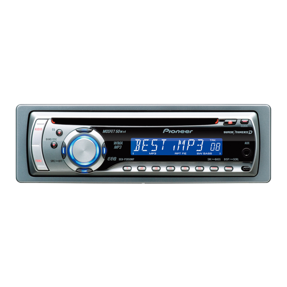
CD RECEIVER
DEH-P3950MP
DEH-P3950MP
This service manual should be used together with the following manual(s):
Model No.
Order No.
CX-3195
CRT3815
For details, refer to "Important Check Points for Good Servicing".
PIONEER CORPORATION
PIONEER ELECTRONICS (USA) INC. P.O. Box 1760, Long Beach, CA 90801-1760, U.S.A.
PIONEER EUROPE NV Haven 1087, Keetberglaan 1, 9120 Melsele, Belgium
PIONEER ELECTRONICS ASIACENTRE PTE. LTD. 253 Alexandra Road, #04-01, Singapore 159936
PIONEER CORPORATION 2006
Mech.Module
S10.5COMP2
CD Mech. Module : Circuit Descriptions, Mech. Descriptions, Disassembly
4-1, Meguro 1-chome, Meguro-ku, Tokyo 153-8654, Japan
DEH-P3950MP/XU/ES
/XU/CN5
Remarks
ORDER NO.
CRT3824
/XU/ES
K-ZZA. OCT. 2006 Printed in Japan
Advertisement
Table of Contents

Related Manuals for Pioneer DEH-P3950MP


Summary of Contents for Pioneer DEH-P3950MP
- Page 1 PIONEER CORPORATION 4-1, Meguro 1-chome, Meguro-ku, Tokyo 153-8654, Japan PIONEER ELECTRONICS (USA) INC. P.O. Box 1760, Long Beach, CA 90801-1760, U.S.A. PIONEER EUROPE NV Haven 1087, Keetberglaan 1, 9120 Melsele, Belgium PIONEER ELECTRONICS ASIACENTRE PTE. LTD. 253 Alexandra Road, #04-01, Singapore 159936 PIONEER CORPORATION 2006 K-ZZA.
-
Page 2: Safety Information
(shorting-solder) by referring to "the DISASSEMBLY". 4. After replacing the pickup unit, be sure to check the grating. 5. Be careful in handling ICs. Some ICs such as MOS type are so fragile that they can be damaged by electrostatic induction. DEH-P3950MP/XU/ES... - Page 3 To protect products from damages or failures during transit, the shipping mode should be set or the shipping screws should be installed before shipment. Please be sure to follow this method especially if it is specified in this manual. DEH-P3950MP/XU/ES...
-
Page 4: Table Of Contents
7. GENERAL INFORMATION ..........................51 7.1 DIAGNOSIS ............................. 51 7.1.1 DISASSEMBLY ............................. 51 7.1.2 CONNECTOR FUNCTION DESCRIPTION ..................54 7.2 PARTS..............................55 7.2.1 IC ................................55 7.2.2 DISPLAY ............................... 65 7.3 OPERATIONAL FLOW CHART ....................... 67 8. OPERATIONS ..............................68 DEH-P3950MP/XU/ES... -
Page 5: Specifications
1. SPECIFICATIONS - DEH-P3950MP/XU/ES DEH-P3950MP/XU/ES... - Page 6 - DEH-P3950MP/XU/CN5 DEH-P3950MP/XU/ES...
- Page 7 DEH-P3950MP/XU/ES...
-
Page 8: Exploded Views And Parts List
• Screw adjacent to mark on the product are used for disassembly. • For the applying amount of lubricants or glue, follow the instructions in this manual. (In the case of no amount instructions,apply as you think it appropriate.) 2.1 PACKING DEH-P3950MP/XU/ES... - Page 9 19-4 Caution Card CRP1310 19-5 Warranty Card See Contrast table(2) Polyethylene Bag CEG1373 Battery CEX1065 (2) CONTRAST TABLE DEH-P3950MP/XU/ES and DEH-P3950MP/XU/CN5 are constructed the same except for the following: Mark Description DEH-P3950MP/XU/ES DEH-P3950MP/XU/CN5 Case Assy CXB3520 Not used Carton YHG5116...
-
Page 10: Exterior
2.2 EXTERIOR DEH-P3950MP/XU/ES... - Page 11 Antenna Jack(CN401) CKX1056 IC(IC1802) GP1UX51RK Holder CND3545 Sheet See Contrast table(2) Holder CND3703 (2) CONTRAST TABLE DEH-P3950MP/XU/ES and DEH-P3950MP/XU/CN5 are constructed the same except for the following: Mark Description DEH-P3950MP/XU/ES DEH-P3950MP/XU/CN5 Panel YNS5190 CNS8762 Tuner Amp Unit YWM5131 YWM5159 Detachable Assy...
-
Page 12: Cd Mechanism Module
2.3 CD MECHANISM MODULE DEH-P3950MP/XU/ES... - Page 13 Bracket CND2583 CND2584 Lever CND2585 CND2586 Bracket CND2587 CND2588 Lever CND2589 Holder CNV7201 Gear CNV7207 Gear CNV7208 Gear CNV7209 Gear CNV7210 Gear CNV7211 Gear CNV7212 Rack CNV7214 CNV7216 Roller CNV8189 Gear CNV7219 Guide CNV7361 Gear CNV7595 Guide CNV8448 CNV7805 DEH-P3950MP/XU/ES...
-
Page 14: Block Diagram And Schematic Diagram
LOAD/ CARRIAGE BRST,BRXEN,BSRQ BRST,BRXEN,BSRQ,BDATA,BSCK MOTOR LCOM CONT CONT BDATA,BSCK Q991 CD VD B.UP Q992 12EJ DSCSNS VDCONT HOME S904 S905 S901 12EJ HOME SWVDD3V S903 DREG Q601 DSCSNS VDSENS EEPROM M-REGC CS,SK IC202 PLL_VDD DI,DO S-93C56BD0I-J8 DVDD3 DVDD2 DVDD4 DEH-P3950MP/XU/ES... -
Page 15: Keyboard Unit
ROT1 ROT1 IC1802 SWVDD SWVDD3V ROT1 GP1UX51RK ROT0 ROT0 ROT0 DREG VOLUME KEY DATA PUSH:SOURCE X1801 M-REGC 5MHz DPDT DPDT DPDT DPDT LCD DRIVER/ PLL_VDD KEY CONTROLLER KYDT KYDT DVDD3 KYDT KYDT IC 1801 DVDD2 VLCD LCD1801 PD6340A DVDD4 DEH-P3950MP/XU/ES... -
Page 16: Overall Connection Diagram(Guide Page)
3.2 OVERALL CONNECTION DIAGRAM(GUIDE PAGE) Note: When ordering service parts, be sure to refer to " EXPLODED VIEWS AND PARTS LIST" or "ELECTRICAL PARTS LIST". Large size SCH diagram CN701 Guide page Detailed page SYSTEM CONTROLLER DEH-P3950MP/XU/ES... - Page 17 12k ohms 10k ohms *Capacitors Code Practical value 0.01uF 101/10 100uF/10V The > mark found on some component parts indicates the importance of the safety factor of the part. Therefore, when replacing, be sure to use parts of identical designation. DEH-P3950MP/XU/ES...
- Page 18 DEH-P3950MP/XU/ES...
- Page 19 DEH-P3950MP/XU/ES...
- Page 20 DEH-P3950MP/XU/ES...
- Page 21 DEH-P3950MP/XU/ES...
-
Page 22: Keyboard Unit
3.3 KEYBOARD UNIT D1803-D1809 D1812-D1816 D1817,D1819 C1804,C1806 R1803,R1804 BUTTON LED D1818 R1810 D1823,D1825 C1807,C1809 R1805,R1806 R1808 D1820,D1821 D1824 R1811 COLOR CL-197HB1-D(CDE) SML-310VT 104YF RED/BLUE VOL SML-310PT SML-310PT SML-310PT GREEN LCD DRIVER/ KEY CONTROLLER (CN5) (ES) DEH-P3950MP/XU/ES... - Page 23 R1810 R1807 MODEL R1811 R1816 DEH-P3950MP/XU/ES DEH-P3950MP/XU/CN5 KEYBOARD UNIT CN831 AUX1 INPUT VOLUME DEH-P3950MP/XU/ES...
-
Page 24: Cd Mechanism Module(Guide Page)
3.4 CD MECHANISM MODULE(GUIDE PAGE) PICKUP UNIT(P10.5)(SERVICE) EEPROM SWITCHES: CD CORE UNIT(S10.5COMP2) S901:HOME SWITCH..ON-OFF S903:DSCSNS SWITCH..ON-OFF S904:12EJ SWITCH.....ON-OFF S905:8EJ SWITCH....ON-OFF The underlined indicates the switch position. M1 CXC7134 SPINDLE MOTOR M2 CXC4026 LOADING/CARRIAGE MOTOR CD DRIVER DEH-P3950MP/XU/ES... - Page 25 CD CORE UNIT(S10.5COMP2) SIGNAL LINE FOCUS SERVO LINE TRACKING SERVO LINE CARRIAGE SERVO LINE SPINDLE SERVO LINE CN651 & DEH-P3950MP/XU/ES...
- Page 26 DEH-P3950MP/XU/ES...
- Page 27 DEH-P3950MP/XU/ES...
- Page 28 DEH-P3950MP/XU/ES...
- Page 29 DEH-P3950MP/XU/ES...
- Page 30 200 ms/div 500 mV/div 2 ms/div 1 V/div %RFAGC 500 mV/div 500 mV/div 500 mV/div 9TIN 500 mV/div Focus Search waveform Track Open waveform 1 Track Jump waveform Ref.: Ref.: Ref.: REFO REFO REFO Mode: Mode: Mode: TEST TEST TEST DEH-P3950MP/XU/ES...
- Page 31 4LOEJ 312SNS 5 V/div 5 V/div 1 V/div 4LOEJ 0FIN 5 V/div 1 V/div Black dot(800 µm) during play 12 cm CD Eject operation 8 cm CD Eject operation Ref.: Ref.: Ref.: REFO Mode: Mode: Mode: Normal Normal Normal DEH-P3950MP/XU/ES...
-
Page 32: Pcb Connection Diagram
For further information for respective destinations, be sure to check with the schematic dia- gram. CORD ASSY 2.Viewpoint of PCB diagrams Capacitor Connector IP-BUS INPUT SIDE A SIDE B Chip Part P.C.Board CN701 CN1801 DEH-P3950MP/XU/ES... - Page 33 SIDE A REAR OUTPUT FRONT OUTPUT OR SUBWOOFER OUTPUT ANTENNA FRONT DEH-P3950MP/XU/ES...
- Page 34 TUNER AMP UNIT SCET TESTIN DEH-P3950MP/XU/ES...
- Page 35 SIDE B >FU 351 (B,129,132) Fuse 3 A CEK1286 DEH-P3950MP/XU/ES...
-
Page 36: Keyboard Unit
4.2 KEYBOARD UNIT KEYBOARD UNIT SIDE A KEYBOARD UNIT SIDE B CN831 DEH-P3950MP/XU/ES... - Page 37 DEH-P3950MP/XU/ES...
-
Page 38: Cd Core Unit(S10.5Comp2)
4.3 CD CORE UNIT(S10.5COMP2) CD CORE UNIT(S10.5COMP2) SIDE A CN651 PICKUP UNIT(P10.5)(SERVICE) LOADING /CARRIAGE MOTOR SPINDLE MOTOR DEH-P3950MP/XU/ES... - Page 39 CD CORE UNIT(S10.5COMP2) SIDE B DEH-P3950MP/XU/ES...
-
Page 40: Electrical Parts List
(B,129,132) Fuse 3 A CEK1286 Q 802 (B,16,26) Transistor DTC114EUA Q 821 (B,27,12) Transistor 2SA1036K AR401 (B,161,109) Surge Protector IMSA-6801-01Y901 > Fuse 10 A CEK1208 Q 822 (B,21,17) Transistor DTC114EUA FM/AM Tuner Unit CWE2025 Q 931 (B,61,112) Transistor 2SC4081 DEH-P3950MP/XU/ES... - Page 41 R 617 (B,133,31) RS1/16S473J C 152 (B,135,96) CKSRYB224K16 R 618 (B,144,39) RS1/16S473J C 153 (B,102,98) CKSRYB105K10 R 619 (B,144,37) RS1/16S104J C 154 (B,133,95) CKSRYB105K10 R 622 (B,127,25) RS1/16S104J C 155 (A,115,113) CEJQ470M10 R 638 (B,156,86) RS1/16S273J C 156 (B,134,99) CKSRYB105K10 DEH-P3950MP/XU/ES...
- Page 42 (B,29,113) IC PD6340A C 626 (B,127,70) CCSRCH270J50 IC 1802 (A,19,161) Remote IC GP1UX51RK D 1803 (A,7,148) LED SML-310VT C 627 (B,131,76) CCSRCH150J50 D 1804 (A,7,155) LED SML-310VT C 628 (B,139,62) CKSRYB102K50 D 1805 (A,40,148) LED SML-310VT C 629 (B,132,57) CCSRCH4R0C50 DEH-P3950MP/XU/ES...
- Page 43 (B,32,127) CKSRYB105K10 C 1810 (B,23,149) CKSRYB472K50 C 1802 (A,25,154) CKSRYF104Z25 C 1811 (B,23,151) CKSRYB472K50 C 1803 (B,19,159) CKSYF106Z10 C 1810 (B,23,149) CKSRYB472K50 C 1811 (B,23,151) CKSRYB472K50 Unit Number : (CN5) Unit Name : Keyboard Unit Unit Number : CWX3350 DEH-P3950MP/XU/ES...
- Page 44 (A,27,63) RAB4CQ104J R 307 (A,34,19) RS1/16SS183J R 308 (A,38,20) RS1/16SS183J R 309 (A,35,21) RS1/16SS183J R 310 (A,38,21) RS1/16SS183J R 601 (B,28,38) RS1/16SS0R0J R 602 (B,27,41) RS1/16SS0R0J R 606 (B,23,41) RS1/16SS0R0J R 701 (B,16,35) RS1/16SS221J R 702 (A,23,55) RS1/16SS221J CAPACITORS DEH-P3950MP/XU/ES...
-
Page 45: Adjustment
1k ohms in series. • The load and eject operation is not guarantied with the mechanism upside down. If the mechanism is blocked due to mistaken eject operation, reset the product or turn off and on the ACC to restore it. DEH-P3950MP/XU/ES... - Page 46 • When the power is turned on/off the jump mode is reset to the Single TR (91) while the gain of the RFAMP is reset to 0 dB. At the same time all the self-adjusting values shall return to the default setting. DEH-P3950MP/XU/ES...
-
Page 47: Checking The Grating After Changing The Pickup Unit
Because of eccentricity in the disc and a slight misalignment of the clamping center the grating waveform may be seen to "wobble" ( the phase difference changes as the disc rotates). The angle specified above indicates the average angle. • Hint Reloading the disc changes the clamp position and may decrease the "wobble". DEH-P3950MP/XU/ES... - Page 48 Ech → Xch 20 mV/div, AC Grating waveform Fch → Ych 20 mV/div, AC 0° 30° 45° 60° 75° 90° DEH-P3950MP/XU/ES...
-
Page 49: Error Mode
Remarks: Mechanical errors are not displayed (because a CD is turned off in these errors). Unreadable TOC does not constitute an error. An intended operation continues in this case. Upper digits of an error code are subdivided as shown below: 1x: Setup relevant errors, 3x: Search relevant errors, Ax: Other errors. DEH-P3950MP/XU/ES... -
Page 50: System Microcomputer Test Program
TESTIN IC601(Pin 112) terminal to H. The clock signal is output from the SCET IC601(Pin 43) terminal. The frequency of the clock signal is 1 Hz. The clock signal should be 1 Hz ± 0.000 04 Hz. If the clock signal is out of the range, the X'tal (X601) should be replaced with new one. DEH-P3950MP/XU/ES... -
Page 51: General Information
Removing the Tuner Amp Unit (Fig.2) Remove the screw (BSZ26P180FTC). Remove the screw (BSZ26P100FTC). Remove the two screws. Remove the two screws. Straighten the tabs at two locations indicated and then remove the Tuner Amp Unit. Tuner Amp Unit Fig.2 DEH-P3950MP/XU/ES... - Page 52 Upper Frame. 3. While lifting the Carriage Mechanism, remove it from the three Dampers. Caution: When assembling, be sure to apply some alcohol to the Dampers and assemble the mechanism in a clamped state. Damper Damper Carriage Mechanism Lower Frame DEH-P3950MP/XU/ES...
- Page 53 Assemble the sub unit side of the Pickup, taking the plate (Chassis) in-between. When treating the leads of the Load Carriage Motor Assy, do not make them loose over the Feed Screw. Poly Washer Change Arm Pickup Lock Arm Inner Holder Feed Screw Planet Gear Pickup Rack Chassis Pickup DEH-P3950MP/XU/ES...
-
Page 54: Connector Function Description
7.1.2 CONNECTOR FUNCTION DESCRIPTION DEH-P3950MP/XU/ES... -
Page 55: Parts
7.2 PARTS 7.2.1 IC HA12241FP -BUS +BUS BIAS DRIVER OUTPUT (current) PAL007C RECEIVER OUTPUT R out DEH-P3950MP/XU/ES... - Page 56 PML015B - Block Diagram - Pin Layout IN1_L IN1_R IN2_L IN2_R IN3_L IN3_R IN4+_L IN4+_R IN4-_R IN4-_L Front_R Front_L Rear_L Rear_R Vref DATA FIE_R FIE_L Pre/SW_R Pre/SW_L LMout PGND Pref DEH-P3950MP/XU/ES...
- Page 57 Terminal for TUNER only PLL_VDD bu_reset Backup circuit reset input Terminal for TUNER only DVDD3 Terminal for TUNER only DGND2 Terminal for TUNER only L_OUT Terminal for TUNER only R_OUT COMP Terminal for TUNER only Terminal for TUNER only DEH-P3950MP/XU/ES...
- Page 58 VDD for port BVDD DVDDD4 DGND3 E.VOL strobe output E.VOL data output E.VOL clock output CD mechanism power supply output VDCONT Not used Self-rewriting applied voltage input 1(fixed to L) FLMD1 Not used KEYD Wired remote control input Not used 131,132 DEH-P3950MP/XU/ES...
- Page 59 - Block Diagram +BUP Overvoltage Overvoltage Protection Protection (All Ourput OFF) (OFF except VDD) Pre Reg Vref SW5VCONT SW5V SYSPW SYS+B - Pin Layout VDDCONT SWVDD +BUP BSENS SYS+B SWVDD Reduced-voltage Detection SW5V SW5VCONT SYSPW BSENS VDDCONT Overvoltage Detection DEH-P3950MP/XU/ES...
- Page 60 Not used KST4 Key strobe output 29-32 Not used 33-55 SEG35-13 LCD segment output Power supply 57-64 SEG12-5 LCD segment output PD6340A GP1UX51RK - Block Diagram - Pin Layout Demodulato Integrator Comparator Limiter B.P.F vout GND VCC GND VCC vout DEH-P3950MP/XU/ES...
- Page 61 Power supply for the crystal oscillator X.VDD Power supply for DAC DA.VDD Output of audio for the left channel LOUT Ground for DAC DA.GND Connected to the capacitor for band gap REGC Ground for DAC DA.GND ROUT Output of audio for the right channel DEH-P3950MP/XU/ES...
- Page 62 Output of reference voltage REFOUT Reversal input of FE Output of FE ADCIN FE,TE A/D converter input Reversal input of TE Output of TE Output of LD Input of PD AD.VDD Power supply for servo ADC Ground for servo ADC AD.GND DEH-P3950MP/XU/ES...
- Page 63 Output pin for preamplifier for thread OPINLSL Input pin for preamplifier for thread OPOUT3 CH3 preamplifier output pin OPIN3(-) Input pin for inverting input for CH3 preamplifier OPIN3(+) Input pin for non-inverting input for CH3 preamplifier PREVCC PreVcc BA5839FP DEH-P3950MP/XU/ES...
- Page 64 Chip enable for FE_IC "High" active 18 DO Data Out Data output 19 CE2 Chip Enable-2 Chip enable for EEPROM "Low" active. in power ON/OFF, please turn CE2 into "High" (= VDD). 20 SLOUT Signal Level Output Output of FM/AM signals level (D.C.) DEH-P3950MP/XU/ES...
-
Page 65: Display
7.2.2 DISPLAY - LCD(CAW1931)(DEH-P3950MP/XU/ES) DEH-P3950MP/XU/ES... - Page 66 - LCD(CAW1930)(DEH-P3950MP/XU/CN5) DEH-P3950MP/XU/ES...
-
Page 67: Operational Flow Chart
In case of the above signal, the communication Source keys with Grille microcomputer may fail. operative If the time interval is not 300 msec, the oscillator may be defective. Source ON SYSPW←H Pin 15 Completes power-on operation.(After that, proceed to each source operation.) DEH-P3950MP/XU/ES... -
Page 68: Operations
8. OPERATIONS DEH-P3950MP/XU/ES... - Page 69 (CXX2204) DEH-P3950MP/XU/ES...
- Page 70 - Connection Diagram DEH-P3950MP/XU/ES...
- Page 71 DEH-P3950MP/XU/ES...
- Page 72 CD Mechanism Module Before shipping out the product, be sure to clean the following portions by using the prescribed cleaning tools: Portions to be cleaned Cleaning tools CD pickup lenses Cleaning liquid : GEM1004 Cleaning paper : GED-008 g p p DEH-P3950MP/XU/ES...