Table of Contents
Advertisement
Quick Links
Advertisement
Table of Contents

Related Manuals for National Instruments Isolated Analog Input Device NI PXI-4224


Summary of Contents for National Instruments Isolated Analog Input Device NI PXI-4224
- Page 1 NI PXI-4224 User Manual NI PXI-4224 User Manual August 2008 373752G-01...
- Page 2 Thailand 662 278 6777, Turkey 90 212 279 3031, United Kingdom 44 (0) 1635 523545 For further support information, refer to the Signal Conditioning Technical Support Information document. To comment on National Instruments documentation, refer to the National Instruments Web site at ni.com/info and enter the info code feedback.
-
Page 3: Important Information
Instruments Corporation. National Instruments respects the intellectual property of others, and we ask our users to do the same. NI software is protected by copyright and other intellectual property laws. Where NI software may be used to reproduce software or other materials belonging to others, you may use NI software only to reproduce materials that you may reproduce in accordance with the terms of any applicable license or other legal restriction. - Page 4 Conventions The following conventions are used in this manual: <> Angle brackets that contain numbers separated by an ellipsis represent a range of values associated with a bit or signal name—for example, AO <3..0>. » The » symbol leads you through nested menu items and dialog box options to a final action.
-
Page 5: Table Of Contents
Contents Chapter 1 About the NI PXI-4224 What You Need to Get Started ...1-2 National Instruments Documentation ...1-3 Installing the Application Software, NI-DAQ, and the DAQ Device ...1-3 Installing the NI PXI-4224 ...1-4 LED Pattern Descriptions ...1-4 Chapter 2 Connecting Signals Connecting Signals to the NI PXI-4224 ...2-1... - Page 6 Contents Chapter 5 Using the NI PXI-4224 Developing Your Application ... 5-1 Typical Program Flow Chart... 5-1 Overview of Typical Flow Chart ... 5-3 Creating a Task Using DAQ Assistant or Programmatically ... 5-3 Adjusting Timing and Triggering... 5-3 Configuring Channel Properties ... 5-4 Acquiring, Analyzing, and Presenting...
- Page 7 Figure B-10. AI CONV CLK Output Signal Timing ...B-8 Figure B-11. AI SAMPLE CLK TIMEBASE Signal Timing ...B-9 Figure B-12. AI HOLD COMPLETE Signal Timing...B-10 Figure C-1. Injector/Ejector Handle Position Before Device Removal...C-2 © National Instruments Corporation Contents NI PXI-4224 User Manual...
- Page 8 Contents Tables Table 2-1. NI PXI-4224 25-Pin D-SUB Terminal Pin Assignments ... 2-2 Table 4-1. Signal Conditioning Functional Blocks ... 4-3 Table 4-2. PXI Trigger Bus Timing Signals ... 4-9 Table 5-1. NI-DAQmx Properties ... 5-4 Table 5-2. Programming a Task in LabVIEW ... 5-6 Table 5-3.
-
Page 9: About The Ni Pxi-4224
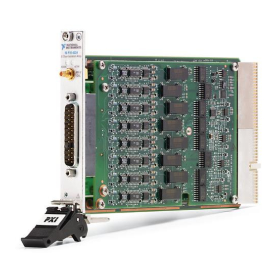
The NI PXI-4224 is configured using Measurement & Automation Explorer (MAX) or through function calls to NI-DAQmx. Note The NI PXI-4224 is supported in NI-DAQmx only. © National Instruments Corporation Each channel has a gain of either 1 or 10. An isolation rating of 42.4 V peak The front connector is a 25-pin D-SUB connector, with 16 pins for analog input. -
Page 10: What You Need To Get Started
Chapter 1 About the NI PXI-4224 What You Need to Get Started To set up and use the NI PXI-4224, you need the following: ❑ ❑ ❑ ❑ You can download NI documents from NI PXI-4224 User Manual Hardware – NI PXI-4224 –... -
Page 11: National Instruments Documentation
NI PXI-4224 device. If you do not have NI-DAQ 7.3.1 or later, you can either contact an NI sales representative to request it on a CD or download it from © National Instruments Corporation DAQ Getting Started Guide—This document describes how to install NI-DAQ devices and NI-DAQ. Install NI-DAQmx before you install the SCXI module. -
Page 12: Installing The Ni Pxi-4224
Chapter 1 About the NI PXI-4224 Installing the NI PXI-4224 Refer to the Read Me First: Radio-Frequency Interference document before Note removing equipment covers or connecting or disconnecting any signal wires. Refer to the DAQ Getting Started Guide to unpack, install, and configure the NI PXI-4224 in a PXI chassis, and then to the SCXI Quick Start Guide if you are using a PXI/SCXI combination chassis. -
Page 13: Connecting Signals
Table 2-1 to make the signal connections if you are constructing a connector using a 25-pin D-SUB connector. Connect a timing or triggering signal to the PFI 0/CAL SMB connector using a cable with an SMB signal connector. © National Instruments Corporation NI PXI-4224 User Manual... -
Page 14: Table 2-1. Ni Pxi-4224 25-Pin D-Sub Terminal Pin Assignments
Chapter 2 Connecting Signals The PFI 0/CAL SMB connector is for low-voltage timing and calibration signals Caution only. Voltages greater than ±15 V can damage the device. If you are building a 25-pin D-SUB connector for your application, make sure you use a connector and wires that are safety rated for the voltage and category of the signals in your application. -
Page 15: Analog Input Connections
NI PXI-4224, and electrical diagrams showing the signal source and connections. Whenever possible, use shielded twisted-pair field wiring and grounding to reduce the effects of unwanted noise sources. © National Instruments Corporation Chapter 2 NI PXI-4224 8 Chan Isolation Amp... -
Page 16: Figure 2-2. Unshielded Floating Signal Source Connection Using A D-Sub Connector
Chapter 2 Connecting Signals In the electrical diagrams, two different ground symbols are used. These symbols indicate that you cannot assume that the indicated grounds are at the same potential. Refer to Appendix A, Specifications, for maximum working voltage specifications. You can make signal connections to the NI PXI-4224 through either an NI terminal block, such as the TB-2725, or you can build a connector using a 25-pin D-SUB. -
Page 17: Figure 2-3. Unshielded Grounded Signal Source Connection Using A D-Sub Connector
Signal Source – Ground Reference Figure 2-3. Unshielded Grounded Signal Source Connection Using a D-SUB Connector © National Instruments Corporation Twisted-Pair Wiring Chapter 2 Connecting Signals CH 0 AI 0 + AI 0 – CH 7 AI 7 + AI 7 –... -
Page 18: Figure 2-4. Shielded Floating Signal Source Connection Using A D-Sub Connector
Chapter 2 Connecting Signals Signal Source – Figure 2-4. Shielded Floating Signal Source Connection Using a D-SUB Connector NI PXI-4224 User Manual Twisted-Pair Shielding Wiring CH 0 AI 0 + AI 0 – CH 7 AI 7 + AI 7 – ni.com... -
Page 19: Figure 2-5. Shielded Grounded Signal Source Connection Using A D-Sub Connector
Signal Source – Ground Reference Figure 2-5. Shielded Grounded Signal Source Connection Using a D-SUB Connector © National Instruments Corporation Twisted-Pair Shielding Wiring Chapter 2 Connecting Signals CH 0 AI 0 + AI 0 – CH 7 AI 7 + AI 7 –... -
Page 20: Figure 2-6. Unshielded Floating Signal Source Connection Using A Terminal Block
Chapter 2 Connecting Signals Figures 2-6 through 2-9 illustrate connecting signals using a terminal block. Signal Source – Figure 2-6. Unshielded Floating Signal Source Connection Using a Terminal Block NI PXI-4224 User Manual Terminal Block Twisted-Pair Wiring CH 0 AI 0 + AI 0 –... -
Page 21: Figure 2-7. Unshielded Grounded Signal Source Connection Using A Terminal Block
Signal Source – Ground Reference Figure 2-7. Unshielded Grounded Signal Source Connection Using a Terminal Block © National Instruments Corporation Terminal Block Twisted-Pair Wiring Chapter 2 Connecting Signals CH 0 AI 0 + AI 0 – CH 7 AI 7 + AI 7 –... -
Page 22: Figure 2-8. Shielded Floating Signal Source Connection Using A Terminal Block
Chapter 2 Connecting Signals Twisted-Pair Wiring Signal Source – Figure 2-8. Shielded Floating Signal Source Connection Using a Terminal Block NI PXI-4224 User Manual Shielding Terminal Block 2-10 CH 0 AI 0 + AI 0 – CH 7 AI 7 + AI 7 –... -
Page 23: Floating Signal Source Connection
To connect a floating signal source connection to the NI PXI-4224, the signal (V signal reference (V © National Instruments Corporation Shielding Terminal Block +) is connected to the NI PXI-4224 channel (AI X +). The –) is connected to the channel reference (AI X –). -
Page 24: Ground-Referenced Signal Connection
Chapter 2 Connecting Signals Ground-Referenced Signal Connection Figures 2-3, 2-5, 2-7, and 2-9 illustrate the ground-referenced signal connection. In this configuration, the voltage source being measured is referenced to its own ground reference that is connected through a conductive path to the instrument ground reference. For example, the path can be through a common earth ground or through the power line ground. -
Page 25: Configuring And Testing
To measure scaled voltages, further configure channel properties, and configure timing settings, use an NI-DAQmx Task or NI-DAQmx Global Channel. © National Instruments Corporation Expand Devices and Interfaces to display the list of devices and interfaces. Expand NI-DAQmx Devices to display the list of NI-DAQmx devices. -
Page 26: Configuring The Ni Pxi-4224 In Max
Chapter 3 Configuring and Testing Configuring the NI PXI-4224 in MAX This section describes how to create NI-DAQmx Tasks and NI-DAQmx Global Channels in MAX that allow you to take measurements with the NI PXI-4224. Creating a Voltage Task or Global Channel Using NI-DAQmx An NI-DAQmx Global Channel gives a physical channel a name and provides scaling. -
Page 27: Verifying And Self-Testing An Ni-Daqmx Task Or Global Channel
You have now verified the NI PXI-4224 configuration and signal connection. © National Instruments Corporation If you created an NI-DAQmx Task, set the timing and triggering settings you wish to use in the test in the Task Timing and Task Triggering tabs. -
Page 28: Theory Of Operation
This chapter describes the theory of operation, measurement considerations, and timing information. Theory of Operation Figure 4-1 illustrates the key functional components of the NI PXI-4224, including the DAQ and integrated signal conditioning circuitry. © National Instruments Corporation NI PXI-4224 User Manual... -
Page 29: Figure 4-1. Block Diagram Of Ni Pxi-4224
Chapter 4 Theory of Operation Connector Figure 4-1. Block Diagram of NI PXI-4224 NI PXI-4224 User Manual ni.com... -
Page 30: Signal Conditioning Functional Overview
200 kΩ does not interfere with the accuracy of the measurement. For example, a 200 kΩ source impedance results in a 0.02% gain error. © National Instruments Corporation Description Each NI PXI-4224 channel has overvoltage protection in the event that a channel is improperly wired. -
Page 31: Common-Mode Rejection Ratio
Chapter 4 Theory of Operation Signal Source Source Impedance – Although R measuring AC signals since C large. For example: Common-Mode Rejection Ratio The ability of a measurement device to reject voltages that are common to both input terminals is referred to as the common-mode rejection ratio (CMRR). -
Page 32: Effective Cmr
These timing signals also can be controlled by signals internally generated to the DAQ-STC, and these signals are software configurable. Figure 4-3 shows an example of the signal routing multiplexer controlling the AI CONVERT CLOCK signal. © National Instruments Corporation Chapter 4 Theory of Operation NI PXI-4224 User Manual... -
Page 33: Programmable Function Inputs
Chapter 4 Theory of Operation Figure 4-3 shows that AI CONV CLK can be generated from a number of sources, such as the external signals PFI 0, PXI_Trig<0..5>, and PXI_Star, and the Ctr 0 Internal Output. Programmable Function Inputs PFI 0 is connected to the front SMB connector of the NI PXI-4224. Software can select PFI 0 as the external source for a given timing signal. -
Page 34: Device And Pxi Clocks
Star Trigger controller plugged into slot 2 of the chassis. For more information about the Star Trigger, refer to the PXI Hardware Specification, Revision 2.1 and PXI Software Specification, Revision 2.1. © National Instruments Corporation Chapter 4 with other devices. Master Timebase... -
Page 35: Figure 4-4. Ni Pxi-4224 Pxi Trigger Bus Signal Connection
Chapter 4 Theory of Operation Figure 4-4 shows this signal connection scheme. NI PXI-4224 User Manual PXI Trigger<0..5> PXI Star PXI Trigger<7> Switch Figure 4-4. NI PXI-4224 PXI Trigger Bus Signal Connection DAQ-STC AI START TRIG AI REF TRIG AI CONV CLK AI SAMP CLK AI PAUSE TRIG AI SAMPLE CLK TIMEBASE... -
Page 36: Table 4-2. Pxi Trigger Bus Timing Signals
AI SAMPLE CLK Input TIMEBASE AI HOLD Output COMPLETE © National Instruments Corporation Table 4-2. PXI Trigger Bus Timing Signals Description This trigger is the source for the analog input digital start trigger, which is the trigger that begins an acquisition. -
Page 37: Using The Ni Pxi-4224
Figure 5-1 shows a typical program flow chart for creating an AI voltage channel, taking a measurement, and clearing the data. For more information about creating tasks and channels in MAX, refer to Chapter 3, Note Configuring and Testing. © National Instruments Corporation NI PXI-4224 User Manual... -
Page 38: Figure 5-1. Typical Program Flowchart
Chapter 5 Using the NI PXI-4224 Create Task in DAQ Assistant or MAX Further Configure Channels? Configure Channels Start Measurement Read Measurement NI PXI-4224 User Manual Create Task Using DAQ Assistant? Process Data Graphical Display Tools Clear Task Figure 5-1. Typical Program Flowchart Create a Task Programmatically Create AI Voltage Channel... -
Page 39: Overview Of Typical Flow Chart
If you create a task in the DAQ Assistant, you still can modify the timing properties of the task programmatically in your application. © National Instruments Corporation Chapter 5 Using the NI PXI-4224 NI PXI-4224 User Manual... -
Page 40: Configuring Channel Properties
Chapter 5 Using the NI PXI-4224 When programmatically adjusting timing settings, you can set the task to acquire continuously, acquire a buffer of samples, or acquire one point at a time. For continuous and buffered acquisitions, you can set the acquisition rate and the number of samples to read. -
Page 41: Acquiring, Analyzing, And Presenting
Except where otherwise stated, the VIs in Table 5-2 are located on the Functions» Note All Functions»NI Measurements»DAQmx - Data Acquisition subpalette and accompanying subpalettes in LabVIEW. © National Instruments Corporation Chapter 5 Using the NI PXI-4224 NI PXI-4224 User Manual... -
Page 42: Table 5-2. Programming A Task In Labview
Chapter 5 Using the NI PXI-4224 Flowchart Step Create Task in DAQ Assistant Create a Task Programmatically (optional) Create AI Voltage Channel (optional) Adjust Timing Settings (optional) Configure Channels (optional) Start Measurement Read Measurement Analyze Data Display Data NI PXI-4224 User Manual Table 5-2. -
Page 43: Using A Daqmx Channel Property Node In Labview
Note If you do not use Active Channels, the properties will be set on all of the channels in the task. © National Instruments Corporation VI or Program Step For continuous sampling, use a While Loop. If you are using hardware timing, you also need to set the sample mode to Continuous Samples. -
Page 44: Synchronization And Triggering
Chapter 5 Using the NI PXI-4224 Note Refer to the LabVIEW Help for information about property nodes and specific NI-DAQmx properties. Synchronization and Triggering If you have multiple NI PXI-4224 devices, you can synchronize them to acquire samples at the same time and at the same rate. You can use multiple NI PXI-4224 devices to acquire and analyze complex signals. -
Page 45: Figure 5-2. General Synchronizing Flowchart
Rate from Master Task Create a Slave Task (optional) Create Slave AI Voltage Channels Configure Slave Channel More Slave Tasks? © National Instruments Corporation Configure Slave Timing Timebase from Master Configure Slave Triggering Start Slave Measurement(s) Start Master Measurement Read Measurement Continue Sampling? Clear Master Task, Figure 5-2. -
Page 46: Synchronizing The Ni Pxi-4224 Using Labview
Chapter 5 Using the NI PXI-4224 Synchronizing the NI PXI-4224 Using LabVIEW This section describes in more detail the steps shown in Figure 5-2, such as how to create a task in LabVIEW and configure the channels of the NI PXI-4224. For further instructions, select Help»VI, Function, & How-To Help from the LabVIEW menu bar. -
Page 47: Other Application Documentation And Material
• • • © National Instruments Corporation VI or Program Step Use a DAQmx Timing Property Node to set MasterTimebase.Src values retrieved from the master task in the Source and Rate from Master Task (Start Digital Edge) use DAQmx Trigger.vi... -
Page 48: Calibrating The Ni Pxi-4224
Chapter 5 Using the NI PXI-4224 Calibrating the NI PXI-4224 Calibration refers to the process of minimizing measurement errors. On the NI PXI-4224, errors from the digitizer components of the DAQ device circuitry are corrected in the analog circuitry by onboard calibration digital-to-analog converters (CalDACs). -
Page 49: External Calibration
You can download all available external calibration documents by going to ni.com/calibration NI recommends you perform an external calibration once a year. © National Instruments Corporation Right-click the NI PXI-4224 and select Self-Calibrate. A dialog box opens indicating that the NI PXI-4224 is self-calibrating. -
Page 50: Table A-1. Maximum Sampling Rates
Analog Input Number of input channels ... 8 Input range ... ±10 VDC Resolution ... 16 bits Maximum sampling rate ... 200 kS/s aggregate multichannel © National Instruments Corporation Table A-1. Maximum Sampling Rates Number of Channels or 60 VDC max... - Page 51 Appendix A Specifications for Input coupling...DC Bandwidth, –3 dB ...15 kHz Slew rate ...2 V/μs typical Input impedance Input bias current ...100 pA CMRR Crosstalk at 1 kHz Accuracy Nominal % of Range Reading Offset 1 Year (μV) ±10 V 0.11 ±1730 ±1 V...
- Page 52 Source... PFI 0/AI START TRIG Compatibility ... 5 V/TTL The pre-calibration errors apply only to users doing register level programming. Pre-calibration errors are not visible to NI-DAQmx users. © National Instruments Corporation Signal conditioning component only... ±50 mV typ, ±160 mV max Signal conditioning component only...
-
Page 53: Figure A-1. Pxi-4224 Dimensions
Appendix A Specifications for Response ...Rising or falling edge, Pulse width ...10 ns min Impedance...10 kΩ Coupling ...DC PXI Trigger Bus Trigger lines...6 Star trigger ...1 PCI Bus Interface Master, slave Power Requirements 2 A at +5 VDC (±5%) Physical (0.79 in.) NI PXI-4224 User Manual 2.0 cm... - Page 54 Storage temperature ... –40 to 70 °C Humidity ... 10 to 90% RH, noncondensing Maximum altitude ... 2,000 m Pollution Degree (indoor use only) ... 2 © National Instruments Corporation or 60 VDC. Do not use this device for connection to peak Continuous ... 60 VDC, Withstand ...
- Page 55 Appendix A Specifications for Safety This product meets the requirements of the following standards of safety for electrical equipment for measurement, control, and laboratory use: • • Note For UL and other safety certifications, refer to the product label or the Online Product Certification section.
- Page 56 Waste Electrical and Electronic Equipment (WEEE) At the end of the life cycle, all products must be sent to a WEEE recycling EU Customers center. For more information about WEEE recycling centers and National Instruments WEEE initiatives, visit National Instruments...
- Page 57 In level-detection mode, there are no pulse width requirements imposed by the PFIs themselves. Limits can be imposed by the particular timing signal being controlled. These requirements are listed in the sections that describe the signals. © National Instruments Corporation Theory of Operation. NI PXI-4224 User Manual...
-
Page 58: Figure B-1. Typical Posttriggered Sequence
Appendix B Timing Signal Information DAQ Timing Connections The timing signals are AI START TRIG, AI REF TRIG, AI SAMP CLK, AI CONV CLK, AI PAUSE TRIG, AI SAMPLE CLK TIMEBASE, and AI HOLD COMPLETE. Posttriggered DAQ allows you to view data that is acquired after a trigger event is received. -
Page 59: Figure B-3. Ai Start Trig Input Signal Timing
Figures B-3 and B-4 show the input and output timing requirements for AI START TRIG. Rising-Edge Falling-Edge © National Instruments Corporation Polarity Polarity Figure B-3. AI START TRIG Input Signal Timing = 50 to 100 ns Figure B-4. AI START TRIG Output Signal Timing... -
Page 60: Figure B-5. Ai Ref Trig Input Signal Timing
Appendix B Timing Signal Information The device also uses AI START TRIG to initiate pretriggered operations. In pretriggered applications, AI START TRIG is generated by a software trigger unless a PFI pin is selected as the source of AI START TRIG. Refer to the AI REF TRIG Signal section for a complete description of the use of AI START TRIG and AI REF TRIG in a pretriggered operation. -
Page 61: Figure B-6. Ai Ref Trig Output Signal Timing
AI SAMP CLK is deasserted, t , after the last conversion in the scan is initiated. This output is set to high-impedance at startup. © National Instruments Corporation NI PXI-4224 User Manual... -
Page 62: Figure B-7. Ai Samp Clk Input Signal Timing
Appendix B Timing Signal Information Figures B-7 and B-8 show the input and output timing requirements for AI SAMP CLK. Rising-Edge Falling-Edge The AI CONV CLK pulses are masked off until the device generates AI SAMP CLK. If you use internally generated conversions, the first AI CONV CLK appears when the onboard SI2 counter reaches zero. -
Page 63: Figure B-9. Ai Conv Clk Input Signal Timing
50 to 100 ns. This output is set to high-impedance at startup. Figures B-9 and B-10 show the input and output timing requirements for AI CONV CLK. Rising-Edge Falling-Edge © National Instruments Corporation Polarity Polarity Figure B-9. AI CONV CLK Input Signal Timing Appendix B... -
Page 64: Figure B-10. Ai Conv Clk Output Signal Timing
Appendix B Timing Signal Information The ADC switches to hold mode within 60 ns of the selected edge. This hold-mode delay time is a function of temperature and does not vary from one conversion to the next. Separate the AI CONV CLK pulses by at least one conversion period. -
Page 65: Figure B-11. Ai Sample Clk Timebase Signal Timing
Either the 20 MHz or 100 kHz internal timebase generates AI SAMPLE CLK TIMEBASE unless you select an external source. Figure B-11 shows the timing requirements for AI SAMPLE CLK TIMEBASE. © National Instruments Corporation Appendix B = 50 ns minimum = 23 ns minimum Figure B-11. -
Page 66: Figure B-12. Ai Hold Complete Signal Timing
Appendix B Timing Signal Information AI HOLD COMPLETE Signal AI HOLD COMPLETE is an output-only signal that generates a pulse with the leading edge occurring approximately 50 to 100 ns after an A/D conversion begins. The polarity of this output is software configurable, but the polarity is typically configured so that a low-to-high leading edge can clock external analog input multiplexers that indicate when the input signal has been sampled and can be removed. - Page 67 The next time you restart the computer the NI PXI-4224 will have a red circle with a white X inside it next to the device in MAX. © National Instruments Corporation Power off the PXI chassis. Do not remove the NI PXI-4224 device from a chassis that is powered on.
-
Page 68: Figure C-1. Injector/Ejector Handle Position Before Device Removal
Appendix C Removing the NI PXI-4224 Removing the NI PXI-4224 from MAX To remove an NI PXI-4224 device from MAX, complete the following steps after launching MAX: The NI PXI-4224 is now removed from the list of installed devices in MAX. NI PXI-4224 User Manual Figure C-1. - Page 69 How do I program the NI PXI-4224? Refer to Chapter 4, application programming information. There is no register-level programming manual available for the NI PXI-4224. © National Instruments Corporation Go to ni.com Follow the link, Download Software»Drivers and Updates» Search Drivers and Updates.
- Page 70 Appendix D Common Questions How do I perform an external calibration of the NI PXI-4224? As of the NI PXI-4224 release, an external calibration document is not available. To check the availability of an NI PXI-4224 external calibration document is go to Procedures.
- Page 71 Symbols Per. ° Degree. Percent. Positive of, or plus. – Negative of, or minus. Ω Ohm. Amperes. Analog-to-digital. Alternating current. © National Instruments Corporation Value –12 –9 – 6 –3 tera NI PXI-4224 User Manual...
- Page 72 Glossary Analog-to-digital converter—An electronic device, often an integrated circuit, that converts an analog voltage to a digital number. Application development environment. Analog input. AI CONV CLK Convert signal. AI HOLD COMPLETE Scan clock signal. AI PAUSE TRIG Analog input gate signal. AI SAMP CLK Start scan signal.
- Page 73 An analog input consisting of two terminals, both of which are isolated from computer ground, the difference of which is measured. Digital input/output. dithering The addition of Gaussian noise to an analog input signal. © National Instruments Corporation (V1/V2), for signals in volts. Glossary NI PXI-4224 User Manual...
- Page 74 Glossary Direct memory access—A method by which data can be transferred to/from computer memory from/to a device or memory on the bus while the processor does something else. DMA is the fastest method of transferring data to/from computer memory. Differential nonlinearity—A measure in least significant bit of the worst-case deviation of code widths from their ideal value of 1 LSB.
- Page 75 The interchannel delay is regulated by AI CONV CLK. Kilo—The standard metric prefix for 1,000, or 10 measure such as volts, hertz, and meters. 1,000 samples. © National Instruments Corporation , used with units of Glossary NI PXI-4224 User Manual...
- Page 76 Glossary LabVIEW Laboratory Virtual Instrument Engineering Workbench—A program development application based on the programming language G and used commonly for test and measurement purposes. Light-emitting diode. linearity The adherence of device response to the equation R = KS, where R = response, S = stimulus, and K = a constant. Least significant bit.
- Page 77 The timing bus that connects PXI DAQ devices directly, by means of connectors built into the backplane of the PXI chassis, for precise synchronization of functions. This bus is functionally equivalent to the RTSI bus for PCI DAQ devices. © National Instruments Corporation Glossary NI PXI-4224 User Manual...
- Page 78 Glossary relative accuracy A measure in LSB of the accuracy of an ADC. It includes all nonlinearity and quantization errors. It does not include offset and gain errors of the circuitry feeding the ADC. resolution The smallest signal increment that can be detected by a measurement system.
- Page 79 PC, that has the functionality of a classic stand-alone instrument; (2) a LabVIEW software device (VI), which consists of a front panel user interface and a block diagram program. Measured voltage. MEAS Volts, root mean square. © National Instruments Corporation Glossary NI PXI-4224 User Manual...
- Page 80 Glossary waveform Multiple voltage readings taken at a specific sampling rate. working voltage The highest voltage with respect to ground that should be applied to an input terminal during normal use, normally well under the breakdown voltage for safety margin. Includes both the signal and common-mode voltages.
- Page 81 (table), 4-9 input signal timing (figure), B-3 output signal timing (figure), B-3 overview, B-3 AI.AutoZeroMode property (table), 5-4 AI.Coupling property (table), 5-4 © National Instruments Corporation analog input connections, 2-3 ground-referenced signal connection (recommended) (figure), 2-12 shielded, 2-12 specifications, A-1...
- Page 82 See application development device and PXI clocks, 4-7 digital trigger specifications, A-3 documentation application development, 5-11 conventions used in the manual, iv National Instruments documentation, 1-3 effective CMR, 4-5 electromagnetic compatibility specifications, A-6 environmental specifications, A-5 external calibration, 5-13, D-2 ni.com...
- Page 83 3-1 measurement considerations common-mode rejection ratio, 4-4 effective CMR, 4-5 input impedance, 4-3 memory specifications, A-3 National Instruments ADE software, 5-1 NI PXI-4224 See also installation See also specifications block diagram of NI PXI-4224, 4-2 calibrating, 5-12 configuring, 5-4...
- Page 84 2-1 timing connections DAQ timing connections, B-2 programmable function input connections, B-1 signal measurement. See measurement considerations SMB connector, 2-1 PFI 0/CAL SMB connector, 4-6 software installation, 1-3 National Instruments ADE software, 1-3 NI-DAQ, 1-3 version required, D-1 ni.com...
- Page 85 See also NI PXI-4224 block diagram of NI PXI-4224, 4-2 timing and control overview, 4-5 timing and triggering, in application development, 5-3 © National Instruments Corporation timing connections DAQ timing connections typical posttriggered acquisition (figure), B-2 typical pretriggered acquisition...