Table of Contents
Advertisement
MITSUBISHI MORTORS
For the mecha part, please refer to the service manual of CD7WMA(211) (2006 JUL.).
FEATURES/SPECIFICATIONS .................................. 2
DETACHABLE KEY BOARD (DKB) PART .......................
RADIO PART ....................................................................
CD, CD CHANGER PART ..................................................
AUDIO & OTHERS PART ..................................................
REAR VIEW and CONNECTORS .............................. 6
SYSTEM CONFIGURATION ....................................... 7
BLOCK DIAGRAM ...................................................... 8
DISASSEMBLING PROCEDURES ...................... 9~11
EXPLODED VIEW and PARTS LIST ........................ 12
MITSUBISHI ELECTRIC CORP. SANDA WORKS
SE011306093E
SERVICE MANUAL
FM / AM ELECTRONIC TUNING RADIO,
CD PLAYER with CD CHANGER CONTROL
DY-2X64WT-2-TH
Model :
PART No : 8701A053
Your company internal use only
CONTENTS
IC EXPLANATION ............................................... 13~16
ELECTRICAL PARTS LIST ................................. 17,18
3
3
PCB-MAIN.................................................................
4
PCB-PANEL ....................................................................
5
PCB-MAIN................................................................
PCB-PANEL ....................................................................
VOLTAGE ................................................................. 28
WAVEFORM ............................................................. 29
Copyright (c) Mitsubishi Electric Corporation
DY-2X64WT-2-TH
2006 SEP.
19,20
21
22~26
27
Advertisement
Table of Contents

Related Manuals for Mitsubishi DY-2X64WT-2-TH


Summary of Contents for Mitsubishi DY-2X64WT-2-TH
-
Page 1: Table Of Contents
22~26 PCB-MAIN..............SYSTEM CONFIGURATION ........7 PCB-PANEL ..............BLOCK DIAGRAM ............8 VOLTAGE ..............28 DISASSEMBLING PROCEDURES ...... 9~11 WAVEFORM ............. 29 EXPLODED VIEW and PARTS LIST ......12 MITSUBISHI ELECTRIC CORP. SANDA WORKS SE011306093E Copyright (c) Mitsubishi Electric Corporation... -
Page 2: Features/Specifications
FEATURES / SPECIFICATIONS FEATURES SPECIFICATIONS Audio Amp FM Radio Frequency Range : 87.5 ~ 108.0MHz Including high power 4CH Amp. (SEEK:50kHz / STEP:25kHz) Adjustment of BASS,TREBLE, FADER and BALANCE by the audio adjustment button. Intermediate Frequency : 10.7MHz Sensitivity (-3dB Limiting) : Less than 14dB(µV) Sound preset function. -
Page 3: Operation
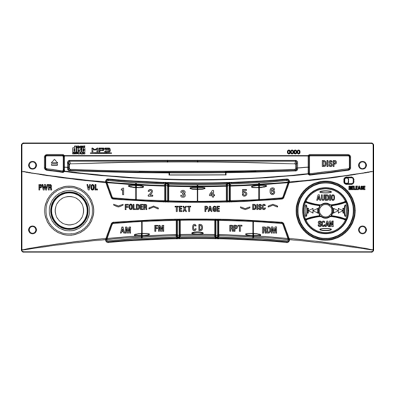
OPERATION DETACHABLE KEY BOARD (DKB) PART ALARM FLASH RELEASE Switch PARTIAL PANEL OUT Detachable Key Board (DKB) Always keep the surface of electric contacts of the Key Board clean to prevent malfunctions due to the dust or rust. To effectively prevent theft of the car stereo, the Control Key Board can be removed rendering the set absolute use- Alarmed Flash less. -
Page 4: Cd, Cd Changer Part
CD, CD CHANGER PART Track Selection Up Button CD Changer Disc Selection Up Button (Push the button less than 0.5 seconds) CD Changer Disc Selection Down Button Fast-forward Button (Push the button 0.5 seconds or more) EJECT Button CD SLOT Track(File) Selection Up Button (MP3) (Push the button 0.5 seconds or more) CD Scan Button... -
Page 5: Audio & Others Part
AUDIO & OTHERS PART AUDIO Control Mode Selection Button AUDIO Control Memory and Preset Channel Button BASS TREBLE FADER BALANCE Memory : Push the button 1.5 seconds or more. Cancel Preset : Push the button less than 1.5 seconds. ID code DISPLAY Button AUDIO Control Up Button AUDIO Control Down Button... -
Page 6: Rear View And Connectors
REAR VIEW and CONNECTORS ANTENNA SOCKET TERMINAL EARTH 4 3 2 1 8 7 6 5 12 11 10 9 14 13 12 11 10 9 8 DIN 13P CD Changer 14P CONNECTOR (P901) 14P CONNECTOR (J802) CONNECTOR (J801) 14P CONNECTOR (P901) 1: Speaker FR ( + ) 6: Speaker RR... -
Page 7: System Configuration
SYSTEM CONFIGURATION Battery Shield Earth Accessory M-SCLK Audio M-BUSY RV Meter (DU-467-1) DY-2X64WT-2-TH M-DATA Shield Earth CD Changer (CD-5000C) Illumination(+) Illumination( _ ) -
Page 8: Block Diagram
BLOCK DIAGRAM... -
Page 9: Disassembling Procedures
DISASSEMBLING PROCEDURES 1. Removal of PLATE-SPR and COVER (See Fig.1) COVER 1) Unscrew the two screws ( 2) Remove the two PLATE-SPR. 4 (M) 3) Unscrew the four screws ( 4) Remove the COVER. PLATE-SPR PLATE-SPR (Fig.1) 2. Removal of CD7 (See Fig.2) 4 (L) 1) Unscrew the four screws ( FLAT-CABLE 18P... - Page 10 3. Removal of HEAT-SINK and BRACKET-DECK (See Fig.3) 1) Unscrew the two screws ( ) and the two screws ( 2) Remove the HEAT-SINK. 3) Remove the two screws ( HEAT-SINK 4) Remove the BRACKET-DECK. 2 (P) 2 (M) BRACKET-DECK (Fig.3) 4.
- Page 11 5. Removal of PCB-MAIN (See Fig.5) 1) Unscrew the two screws ( 2) Unscrew the one screw ( 3) Unscrew the two screws ( ) and the three screws ( 4) Unlatch the five hooks ( a ). 5) Remove the PCB-MAIN. PCB-MAIN 2 (M) (Fig.5)
-
Page 12: Exploded View And Parts List
EXPLODED VIEW and PARTS LIST * : Marked parts are unregistered. Ref. No. Part No. Description Index M014 M007 M002 246L48229 FLAT-CABLE 18P M003 560J26213 CHASSIS-B M011 M004 560J28711 CHASSIS-F M005 *570L46110 SPRING-REL M006 *570L46010 SPRING-REL M007 591K53610 COVER M008 591K40711 BRACKET-DECK M009... -
Page 13: Ic Explanation
IC EXPLANATION IC802 BR93LC56FV Voltage power supply detection Instruction decode Control Clock generation Writing High voltage prohibition generator Address Address 7 bit 7 bit buffer decoder Instruction 2,048 bit register EEPROM array Data 16 bit 16 bit register amp. Dummy bit IC3A1 LA4742 Muting &... - Page 14 IC301 LC75411UES 23 LFIN 22 LFOUT LVref 21 LROUT 20 VSS 19 CL Multiplexer ZERO CROSSDET 18 DI LVref INTERFACE CONTROL LOGIC CIRCUIT CIRCUIT Vref 17 CE RVref Multiplexer ZERO CROSSDET 16 TEST NO SIGNAL TIMMER 15 TIM 14 RROUT RVref 13 RFOUT 12 RFIN...
- Page 15 IC981 S-818A33AUC-BGN-T2G IC804 SN74AHC2G34HDCTR Parasitic DIODE VOUT ON/OFF ON/OFF CIRCUIT Reference Voltage IC805 SN74AHCT244PWR IC980 LF33AB-DT-TR CURRENT LIMIT INHIBIT CONTROL START REFERENCE INHIBIT VOLTAGE DRIVER ERROR AMPLIFIER DUMP PROTECTION TERM. PROTECTION...
- Page 16 IC101 LC72151VS-TRM XBUF PDM1 PHASE DETECTOR REFERENCE CHARGE PUMP DIVIDER PDM2 XOUT TGI1 UNLOCK SWALLOW COUNTER FMIN DETECTOR 1/16,1/17 4bits TGI2 CHARGE PUMP 12bits PROGRAMMABLE AMIN for FAST LOCK DIVIDER AIN2 UNIVERSAL FAST LOCK UP DATA SHIFT REGISTER AOUT2 HCTR/I-3 COUNTER CONTROL LATCH...
-
Page 17: Electrical Parts List
ELECTRICAL PARTS LIST < CHIP PARTS (RESISTORS & CAPACITORS) > Part No. Part No. 103L19xOx 2.0mm 141L06xOx 2.0mm 103L24xOx 3.2mm 141L16xOx 1.6mm 103L29xOx 1.6mm 141L18xOx 1.6mm SOLDERING PART 103P50xOx 1.6mm Ref. No. Part No. Description Ref. No. Part No. Description R12B,13B,976 103L295O1 R-CHIP 150k... - Page 18 Ref. No. Part No. Description Ref. No. Part No. Description D901 264L076O3 DIODE-CHIP AA1101W-740-TR COILS D829 264L037O1 DIODE-CHIP DCC010 L1,910 351L171O3 COIL-CHOKE D852 264P617O1 DIODE-CHIP MC2836T L901 351P11510 COIL-CHOKE D904 264P516O1 DIODE-CHIP S3D6600 L106,113 351P082O4 COIL-CHOKE-CHIP D911 264P583O9 DIODE-Z MA8062H CONNECTORS D931 264L067O3 DIODE-Z-CHIP MA8051M...
-
Page 19: Parts Layout On Printed Circuit Board
PARTS LAYOUT ON PRINTED CIRCUIT BOARD MODEL : DY-2X64WT-2-TH (PARTS SIDE) TO PCB-PANEL (S801) PCB-MAIN... - Page 20 PARTS LAYOUT ON PRINTED CIRCUIT BOARD MODEL : DY-2X64WT-2-TH (PATTERN SIDE) PCB-MAIN PCB-MAIN TO CD-CHANGER TO CD7 TO CENTER DISPLAY...
-
Page 21: Pcb-Panel
PARTS LAYOUT ON PRINTED CIRCUIT BOARD MODEL : DY-2X64WT-2-TH PCB-PANEL (PARTS SIDE) TO PCB-MAIN (PATTERN SIDE) (P801) - Page 22 SCHEMATIC DIAGRAM PCB-MAIN MODEL : DY-2X64WT-2-TH Vol.1 Vol.3 Vol.4 Vol.2...
-
Page 23: Schematic Diagram
SCHEMATIC DIAGRAM PCB-MAIN MODEL : DY-2X64WT-2-TH Vol.1... - Page 24 SCHEMATIC DIAGRAM PCB-MAIN MODEL : DY-2X64WT-2-TH Vol.2...
- Page 25 SCHEMATIC DIAGRAM PCB-MAIN MODEL : DY-2X64WT-2-TH Vol.3...
- Page 26 SCHEMATIC DIAGRAM PCB-MAIN MODEL : DY-2X64WT-2-TH Vol.4...
- Page 27 SCHEMATIC DIAGRAM PCB-PANEL MODEL : DY-2X64WT-2-TH...
-
Page 28: Voltage
VOLTAGE MODEL : DY-2X64WT-2-TH (Pin numbers are as measurement points.) -COM : PD780076GK-699-9ET 3.ELE-VOL IC 4.POWER IC IC801 (PCB-MAIN) IC301 PCB-MAIN IC3A1 PCB-MAIN FM 98.1MHz/AM 999kHz, 30%MOD, VOL MIN FM 83MHz, 30%MOD, VOL MIN FM 83MHz, 30%MOD, VOL MIN BATT, ACC 13.2V BATT, ACC 13.2V... -
Page 29: Waveform
WAVEFORM MODEL : DY-2X64WT-2-TH (Pin numbers are as measurement points.) J802 IC801 J803 (PCB-MAIN) (PCB-MAIN) (PCB-MAIN) CH1=1pin (M-BUSY) CH1=6pin (PLL/VOL CLK) CH1=12pin (CD-DMTS, 3.3Vpp) CH2=8pin (M-SCK) CH2=8pin (PLL/VOL DATA OUT) CH2=14pin (CD-DSTM, 3.3V) CH3=2pin (M-DATA) CH3=5pin (PLL/VOL CE) CH3=15pin (CD-MTS, 3.3V) Vpp=5.0Vpp...