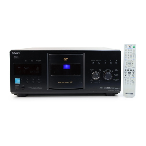
Sony DVP-CX995V Service Manual
Hide thumbs
Also See for DVP-CX995V:
- Operating instructions manual (96 pages) ,
- Specifications (2 pages) ,
- Specifications (2 pages)
Table of Contents
Advertisement
Quick Links
SERVICE MANUAL
Ver. 1.1 2005.12
* Manufactured under license from Dolby
Laboratories. "Dolby," "Pro Logic," and the
double-D symbol are trademarks of Dolby
Laboratories.
** "DTS" and "DTS Digital Surround" are
registered trademarks of Digital Theater
Systems, Inc.
System
Laser: Semiconductor laser
λ = 780 nm for CD
λ = 650 nm for Super Audio CD and
DVD
Emission duration: continuous
Signal format system: NTSC
Audio characteristics
Frequency response: DVD VIDEO (PCM
96 kHz): 2 Hz to 44 kHz (44 kHz: –2 dB
±1 dB), Super Audio CD: 2 Hz to
100 kHz (50 kHz: –3 dB ±1 dB), CD:
2 Hz to 20 kHz (±0.5 dB)
Signal-to-noise ratio (S/N ratio): 115 dB
(LINE OUT AUDIO L/R 1/2 jacks only)
Harmonic distortion: 0.003 %
Dynamic range: DVD VIDEO/Super Audio
CD: 103 dB, CD: 99 dB
Wow and flutter: Less than detected value
(±0.001% W PEAK)
Sony Corporation
9-879-772-02
Home Audio Division
2005L05-1
Published by Sony Engineering Corporation
© 2005.12
DVP-CX995V
Model Name Using Similar Mechanism
CD/DVD Mechanism Type
Base Unit Name
Optical Traverse Unit Name
SPECIFICATIONS
Outputs
(Jack name: Jack type/Output level/Load
impedance)
LINE OUT AUDIO L/R 1/2: Phono jack/
2 Vrms/10 kilohms
DIGITAL OUT (OPTICAL): Optical
output jack/–18 dBm (wave length:
660 nm)
DIGITAL OUT (COAXIAL): Phono jack/
0.5 Vp-p/75 ohms
HDMI OUTPUT: TypeA (19 pin)
5.1CH OUTPUT: Phono jack/2 Vrms/
10 kilohms
COMPONENT VIDEO OUT(Y, P
C
):
R
Phono jack/Y: 1.0 Vp-p/P
/C
B
1)
interlace
= 0.648 Vp-p, progressive or
2)
interlace
= 0.7 Vp-p/75 ohms
1) BLACK LEVEL (COMPONENT
OUT) is ON
2) BLACK LEVEL (COMPONENT
OUT) is OFF
LINE OUT (VIDEO) 1/2: Phono jack/
1.0 Vp-p/75 ohms
S VIDEO OUT 1/2: 4-pin mini DIN/Y:
1.0 Vp-p, C: 0.286 Vp-p/75 ohms
Canadian Model
General
Power requirements:
120 V AC, 60 Hz
Power consumption: 25 W
Dimensions (approx.): 430 × 189 × 545 mm
(17 × 7
× 21
1
/
2
incl. projecting parts
Mass (approx.): 8.6 kg (18 lb 15 oz)
Operating temperature: 5 °C to 35 °C
°
(41
F to 95
Operating humidity: 25 % to 80 %
Supplied accessories
• Audio/video cord
/C
, P
/
B
B
R
(pinplug × 3 y pinplug × 3) (1)
• Remote commander (remote) (1)
, P
/C
:
B
R
R
• Size AA (R6) batteries (2)
Specifications and design are subject to
change without notice.
CD/DVD PLAYER
US Model
NEW
CDM62-DVBU65
DVBU65
DBU-3
1
/
in.) (width/height/depth)
2
°
F)
Advertisement
Table of Contents

Related Manuals for Sony DVP-CX995V


Summary of Contents for Sony DVP-CX995V
- Page 1 OUT) is OFF LINE OUT (VIDEO) 1/2: Phono jack/ 1.0 Vp-p/75 ohms S VIDEO OUT 1/2: 4-pin mini DIN/Y: 1.0 Vp-p, C: 0.286 Vp-p/75 ohms CD/DVD PLAYER Sony Corporation 9-879-772-02 Home Audio Division 2005L05-1 Published by Sony Engineering Corporation © 2005.12...
- Page 2 THE PARTS LIST ARE CRITICAL TO SAFE OPERATION. FONCTIONNEMENT. NE REMPLACER CES COM- POSANTS REPLACE THESE COMPONENTS WITH SONY PARTS WHOSE QUE PAR DES PIÈCES SONY DONT LES NUMÉROS SONT PART NUMBERS APPEAR AS SHOWN IN THIS MANUAL OR DONNÉS DANS CE MANUEL OU DANS LES SUPPLÉMENTS IN SUPPLEMENTS PUBLISHED BY SONY.
-
Page 3: Table Of Contents
DVP-CX995V TABLE OF CONTENTS SERVICING NOTES 7-28. Printed Wiring Boards – PANEL-R Section – ....66 ..........4 7-29. Schematic Diagram – PANEL-R Section – ..... 67 GENERAL ..............9 EXPLODED VIEWS 8-1. Overall Section ..............90 DISASSEMBLY 8-2. Front Panel Section ............91 3-1. -
Page 4: Servicing Notes
DVP-CX995V Ver. 1.1 SECTION 1 SERVICING NOTES NOTES ON HANDLING THE OPTICAL PICK-UP BLOCK OR BASE UNIT The laser diode in the optical pick-up block may suffer electrostatic break-down because of the potential difference generated by the charged electrostatic load, etc. on clothing and the human body. -
Page 5: Region Code
DVP-CX995V may cause the disc to jam or the player to Region code This Player Can Play the malfunction). * CPRM; Content Protection for Recordable Media Your player has a region code printed on the Following Discs is a coding technology that protects copyright for back of the unit and will only play DVD Copy-Once programs. - Page 6 DVP-CX995V ALIGNMENT OF GEAR (CAM) PHASE WITH DOOR CLEANING OF OPTICAL PICK-UP ASS’Y door assy gear (cam) optical pick-up pulley assy Remove the pulley assy, and Align a slit of door assy with a marking on clean the lens of optical pick-up the bottom land of gear tooth when the gear through this hole.
- Page 7 DVP-CX995V When installing the cables, it is made to make it crawl in a chassis. cables DRIVER board cables It is made to contact and for there not to be a switching regulator and cables. AV board AV board cables...
- Page 8 DVP-CX995V SERVICE POSITION – MB board – Connect the jig (J-2501-199-A) to MB board (CN303) and PANEL-L board (CN1003). MB board (CN303) PANEL-L board (CN1003) – Optical pick-up block – optical pick-up block (DVBU65)
-
Page 9: General
DVP-CX995V SECTION 2 This section is extracted from instruction manual. GENERAL • Location of Controls Front panel Front panel display When playing back a DVD VIDEO/DVD-RW Lights up when the player outputs progressive signals Current play mode All discs mode... -
Page 10: Disassembly
DVP-CX995V SECTION 3 DISASSEMBLY • This set can be disassembled in the order shown below. 3-1. DISASSEMBLY FLOW Note 1: The process described in can be performed in any order. Note 2: Without completing the process described in , the next process can not be performed. -
Page 11: Case
DVP-CX995V Note: Follow the disassembly procedure in the numerical order given. 3-2. CASE 5 case 3 three screws (case 3 TP2) 4 two screws (case 3 TP2) 1 two screws (case 3 TP2) 2 two screws (case 3 TP2) 3-3. MB BOARD... -
Page 12: Av Board
DVP-CX995V 3-4. AV BOARD 5 screw (BV3) 6 harness 4 screw (BVTP3 × 8) qf AV board 8 flat type wire (33 core) (CN400) qd connector (CN301) 9 flat type wire (29 core) (CN306) qs connector (CN302) qa connector (CN303) -
Page 13: Front Panel Section
DVP-CX995V 3-6. FRONT PANEL SECTION 2 screw (BVTP3 × 8) 3 two screws (BVTP3 × 8) 4 claw 5 claw 6 front panel section 1 five screws (BVTP3 × 8) 3-7. COVER (PT)/(CDM) 4 six screws (BVTP3 × 8) 6 cover (CDM) 1 screw (BVTP3 ×... -
Page 14: Dvbu65 Assy
DVP-CX995V 3-8. DVBU65 ASSY 1 three screws (BVTP3 × 8) 2 screw (BVTP3 × 8) 5 bracket (top 400) block 3 two screws (BVTP3 × 8) 6 torsion holder 9 DVBU65 assy (magnet) block 0 8 washer 7 washer 8 torsion spring... -
Page 15: Door Assy, Base (Door) Assy
DVP-CX995V 3-10. TABLE (400) ASSY 3 table (400) assy 1 screw (M3 × 14) 2 guide (door) Note: When installing the guide (door), align the positions as shown. 4 10 washer 3-11. DOOR ASSY, BASE (DOOR) ASSY 2 three screws (BVTP3 × 8) -
Page 16: Dc Motor (Door) (M603)
DVP-CX995V 3-12. DC MOTOR (DOOR) (M603) 1 belt (400) 5 DC motor (door) (M603) 4 DOOR MOTOR board 3 Remove two solders. 2 two screws (BVTP3 × 8) 3-13. HOLDER (TABLE SENSOR 400) 2 connector (CN83) 1 four screws (BVTP3 × 6) -
Page 17: Sens Out Board, D. Sens In Board
DVP-CX995V 3-14. D. SENS OUT BOARD, D. SENS IN BOARD 7 screw (PSW3 × 8) 1 screw (PTTWH3 × 6) 8 D. SENS IN board 2 clamp 3 two step screws (T1) 5 screw (PSW3 × 8) 6 D. SENS OUT board 4 bracket (sensor 400) 3-15. -
Page 18: Door Sw Board
DVP-CX995V 3-16. DOOR SW BOARD 1 screw (PTPWH2.6) 3 screw (PTPWH2.6) 5 two screws (BVTP2.6) 2 gear (cam) 6 DOOR SW board 4 gear (B) Precaution during the gear (cam) installation 1 Move the slider (pop-up) and the lever (pu joint) fully 2 Install the gear (cam) in the direction shown in the direction of the arrow A . -
Page 19: Lock Sw Board, Loading Sw Board
DVP-CX995V 3-17. LOCK SW BOARD, LOADING SW BOARD 2 screw (BVTP3 × 8) 1 Rotate the pulley (400) in the direction of the arrow A fully. 3 Rotate the pulley (400) in the direction of the arrow B fully. 7 gear (center) -
Page 20: Cd/Dvd Mechanism Deck Block (Cdm62-Dvbu65)
DVP-CX995V 3-18. CD/DVD MECHANISM DECK BLOCK (CDM62-DVBU65) 6 CD/DVD mechanism deck block (CDM62-DVBU65) 5 seven screws (BVTP3 × 8) 1 connector (CN905) 2 connector (CN903) 4 four screws (BVTP3 × 8) 3 screw (PSW3 × 8) 3-19. MOTOR (400) ASSY (LOADING) (M602)/(TABLE) (M601), LOADING MOTOR BOARD... -
Page 21: Optical Traverse Unit (Dbu-3)
DVP-CX995V 3-20. OPTICAL TRAVERSE UNIT (DBU-3) 8 step screw (M) 7 step screw (M) qd optical traverse unit (DBU-3) qa insulator (RB) 9 step screw (M) 0 insulator (RB) qs insulator (RB) 4 flexible flat cable (CN001) 6 RF TRANSLATION board 5 screw (BVTP2.6) -
Page 22: Test Mode
DVP-CX995V SECTION 4 TEST MODE 0-1. All (All items continuous check) DVD SECTION This menu checks all diagnostic items continuously. Normally, all items are checked successively one after another automatically GENERAL DESCRIPTION unless an error is found, but at a certain item that requires judgment... - Page 23 DVP-CX995V 0-3. Peripheral 1. Drive Auto Adjustment (3-2) Flash Rom Data delete t write t read, and accord check DVD reference disc: Error 32: Delete error Single Layer Error 33: Write error TDV-520CS0 (J-2501-236-A) (NTSC) Error 34: Read data discord...
- Page 24 DVP-CX995V 1-1. DVD Single Layer Disc CD Adjustment Steps Select [1], insert DVD single layer disc, and press [ENTER] key, 1. Sled Reset and the adjustment will be made through the following steps, then 2. Set Disc Type CD adjusted values will be written to the flash memory. The disc slot 3.
- Page 25 DVP-CX995V 20. Auto Focus Balance Adjust L0 1-5. DVD Dual Layer Disc (Opposite) 21. Auto RFEQ Boost Adjust L0 Note: Make sure, using the TDV-540C in this adjustment. 22. Jitter measure Select [5], insert DVD dual layer disc, and press [ENTER] key, and 23.
- Page 26 DVP-CX995V 2. Drive Manual Operation 2-3. Servo Control On the Test Mode Menu screen, select [2], and the manual operation menu will be displayed. For the manual operation, each servo on/ ### Drive Manual Operation ### 3. Servo Control off control and adjustment can be executed manually.
- Page 27 DVP-CX995V [PLAY] 2-6. Memory Check : Loads the disc from the chucking position of The display image is shown below and three screens in total can be Loading In the table toward inside the mechanism deck. selected. When the Disc Load is selected, a series of operation starting from Loading –...
- Page 28 DVP-CX995V Display when [PAUSE] is selected in the Changer Mecha Check. 2-8. Changer Mecha Check On this test mode screen, selecting [8] enables the table sensor and the disc sensor adjustment. The following screen appears. Note: Refer to page 32 for “POP UP MECHANISM ADJUSTMENT”.
- Page 29 DVP-CX995V 3. Mecha Aging DISPLAY SECTION The mechanism aging is not supported. DISPLAY TEST MODE 4. Emergency History Execute the Self Check Mode along the following flow. ### EMG. History ### START Laser Hours I/F CON information xxh xxm xxh xxm FL tube grid and segment check 01.00 00 00 00...
- Page 30 DVP-CX995V 4. FL Tube Grid and Segment Check 6. Key Check First, a grid lights up one after another, and when grid 16 lights up, After the SIRCS reception check finished, the Key check is executed. all grids light up.
- Page 31 DVP-CX995V 7. Jog and LED Check 9. Display Test Mode Result Indication After the Key check finished, the Jog and LED check is executed as After the Keyboard check finished, it displays result of Display Test follows. mode. Upon start of the Jog and LED check, “JOG AND LED” is displayed At this time, even if a signal from a key on the set, remote on the FL tube.
-
Page 32: Mechanical Adjustments
DVP-CX995V SECTION 5 MECHANICAL ADJUSTMENTS POP UP MECHANISM ADJUSTMENT TABLE SENSOR ADJUSTMENT 1. Connect the AC plug of the set to AC consent, then the set After the Pop Up Mechanism Adjustment, perform this adjustment enters standby mode. continuously. 2. Press the [TOP MENU], [CLEAR] and... -
Page 33: Electrical Adjustments
DVP-CX995V SECTION 6 ELECTRICAL ADJUSTMENTS Instruments required: 6-2. POWER SUPPLY CHECK 1) Color monitor TV 2) Oscilloscope 1 or 2 phenomena, band width over 100 MHz, Mode: E-E with delay mode Instrument: Digital voltmeter 3) Frequency counter (over 8 digits) 4) Digital voltmeter EVER +3.3 V Check... - Page 34 DVP-CX995V 6-3-2. Progressive Video Output Level Adjustment 6-3-4. Checking S Video Output S-C <Purpose> <Purpose> This adjusts progressive video output level. If it is incorrect, correct This checks whether the S-C satisfies the NTSC standard. If it is brightness will not be attained when connected to, for instance, not correct, the colors will be to dark or light.
- Page 35 DVP-CX995V 6-3-6. Checking Component Video Output B-Y 6-3-7. Checking Component Video Output R-Y <Purpose> <Purpose> This checks component video output B-Y. If it is incorrect, correct This checks component video output R-Y. If it is incorrect, correct colors will not be displayed when connected to, for instance, colors will not be displayed when connected to, for instance, projector.
- Page 36 DVP-CX995V 6-4. DISC DETECT SENSOR ADJUSTMENT Be sure to perform this adjustment after sensor adjustment in D. SENS OUT board MECHANICAL ADJUSTMENT. (See page 32) Connection: oscilloscope MB board CN301 DSENS_OUT DSENS_OUT: Pin 3 GND: Pin 2 HH_OUT HH_OUT: Pin 1...
- Page 37 DVP-CX995V Adjustment Location: DVP-CX995V...
-
Page 38: Diagrams
DVP-CX995V SECTION 7 DIAGRAMS 7-1. BLOCK DIAGRAM – SERVO Section – RFSACD (Page 39) RFSACD 99 YC0 – YC7 DIGITAL VIDEO (Page 40) YC0 – YC7 RF FILTER RFOUT 4 RFIN OUT-DATA 64 B-DATA Q105 YC_CLK YC_CLKOUT PCM (HDMI) BUFFER... -
Page 39: Block Diagram - Audio Section
DVP-CX995V 7-2. BLOCK DIAGRAM – AUDIO Section – D/A CONVERTER IC501 PCM (5.1CH) FLFR (Page 38) SDTI1 LOUT1+ 2 SDTI2 SLSR LOUT1– 1 SDTI3 LINE AMP MUTING FRONT ADAC_CS IC202 Q203 CSN/CAD1 ROUT1+ 48 CDTI/SDA SCLK CCLK/SCL ROUT1– 47 MUTING... -
Page 40: Block Diagram - Video Section
DVP-CX995V 7-3. BLOCK DIAGRAM – VIDEO Section – WIDE ON/OFF SQUEEZE SWITCH Q103, 104 J103 (2/2) VIDEO LINE OUT 3 VIDEO_IN VIDEO_OUT DIGITAL_VIDEO – YC7 (Page 38) SO2 – SO9 S (2) – S (9) 8 Y_IN Y_OUT YC_CLK 6 C_IN... -
Page 41: Block Diagram - Panel, Table, Power Supply Section
DVP-CX995V 7-4. BLOCK DIAGRAM – PANEL, TABLE, POWER SUPPLY Section – SYSTEM CONTROLLER IC304 (2/2) FL DRIVER RESET SIGNAL IC1001 RESET 16 GENERATOR IC306 OPAMP+B 1G – 15G DA 70 FLDSDATA D301 FLUORESCENT GRID DRIVE CP 69 FLDSCLK INDICATOR TUBE... - Page 42 DVP-CX995V • Note for Printed Wiring Boards and Schematic Diagrams • Circuit Boards Location Note on Printed Wiring Board: Note on Schematic Diagram: • X : parts extracted from the component side. • All capacitors are in µF unless otherwise noted. (p: pF) •...
-
Page 43: Printed Wiring Board - Rf Translation Board
DVP-CX995V • See page 42 for Circuit Boards Location. 7-5. PRINTED WIRING BOARD – RF TRANSLATION Board – : Uses unleaded solder. RF TRANSLATION BOARD SL001 OPTICAL MB BOARD TRAVERSE UNIT CN101 (Page 44) (DBU-3) 1-863-815- (11) DVP-CX995V... -
Page 44: Printed Wiring Board - Mb Board (Side A)
DVP-CX995V • See page 42 for Circuit Boards Location. 7-6. PRINTED WIRING BOARD – MB Board (Side A) – : Uses unleaded solder. • Semiconductor Location (Page 43) (Page 58) (Page 58) Ref. No. Location RF TRANSLATION BOARD AV BOARD... -
Page 45: Printed Wiring Board - Mb Board (Side B)
DVP-CX995V • See page 42 for Circuit Boards Location. 7-7. PRINTED WIRING BOARD – MB Board (Side B) – : Uses unleaded solder. • Semiconductor Location Ref. No. Location MB BOARD (SIDE B) D102 D501 D502 D503 C190 R130 C189... -
Page 46: Schematic Diagram - Mb Section (1/7)
DVP-CX995V • See page 68 for Waveforms. • See page 76 for IC Pin Function Description. 7-8. SCHEMATIC DIAGRAM – MB Section (1/7) – (1/7) 5V-A L104 10µH R124 R180 C126 C142 R110 R117 R127 R139 R145 R151 6.3V 6.3V... -
Page 47: Schematic Diagram - Mb Section (2/7)
DVP-CX995V • See page 69 for IC Block Diagrams. 7-9. SCHEMATIC DIAGRAM – MB Section (2/7) – (2/7) 3.3V-D 5V-D IC101(1/4) C139 R156 LMV324MT/NOPB 0.01 (1/4) CENTRE VOLTAGE GENERATOR IC101(4/4) (4/4) LMV324MT/NOPB (Page 51) REFERENCE VOLTAGE C129 C113 C123 C130 GENERATOR 0.01... -
Page 48: Schematic Diagram - Mb Section (3/7)
DVP-CX995V • See page 68 for Waveforms. • See page 76 for IC Pin Function Description. 7-10. SCHEMATIC DIAGRAM – MB Section (3/7) – (3/7) SMI-DQMU R272 SPDIF TMODE_SW R236 PCM_LRCK (Page 52) R274 R243 4.7k R233 PCM_DATA2 R246 4.7k... -
Page 49: Schematic Diagram - Mb Section (4/7)
DVP-CX995V • See page 69 for IC Block Diagrams. 7-11. SCHEMATIC DIAGRAM – MB Section (4/7) – (4/7) SACD_MCLK SACD_MCLK OSC BUFFER AUD_MCLK (Page 50) IC206 AUD_MCLK SN74LV08APWR SPDIF R642 R619 SPDIF PCM_LRCK PCM_LRCK PCM_SCLK PCM_SCLK PCM_DATA3 R641 R615 FB217... -
Page 50: Schematic Diagram - Mb Section (5/7)
DVP-CX995V • See page 69 for IC Block Diagrams. • See page 76 for IC Pin Function Description. 7-12. SCHEMATIC DIAGRAM – MB Section (5/7) – (5/7) DSD_PCM0 DSD_PCM0 DSD_PCM1 DSD_PCM1 DSD_PCM2 DSD_PCM2 DSD_PCM3 R407 DSD_PCM3 DSD_PCM4 FUR_RST DSD_PCM4 DSD_PCM5... -
Page 51: Schematic Diagram - Mb Section (6/7)
DVP-CX995V • See page 69 for IC Block Diagrams. 7-13. SCHEMATIC DIAGRAM – MB Section (6/7) – (6/7) (Page 52) AMUTE R508 R510 C501 0.001 CN501 BE_RST MUTE_23 (Page 52) MUTE_L PCM_SCLK C505 MUTE_R C503 AUD_MCLK 6.3V D503 AMUTE R501... -
Page 52: Schematic Diagram - Mb Section (7/7)
DVP-CX995V • See page 68 for Waveforms. • See page 76 for IC Pin Function Description. 7-14. SCHEMATIC DIAGRAM – MB Section (7/7) – (7/7) IC306 S-80827CNUA-B8MT WAKE-UP SWITCH Q301,302 IC302 WAKE-UP SWITCH PST9127NL WAKE-UP SWITCH RESET SIGNAL Q302 IC305... -
Page 53: Schematic Diagram - Av Board (1/5)
DVP-CX995V • See page 69 for IC Block Diagrams. • See page 76 for IC Pin Function Description. 7-15. SCHEMATIC DIAGRAM – AV Board (1/5) – (Page 55) (1/5) C412 C417 C422 C402 0.01 0.01 0.01 C401 100 6.3V 3.3V-V (Page 54) +1.8V REGULATOR... -
Page 54: Schematic Diagram - Av Board (2/5)
DVP-CX995V • See page 68 for Waveforms. • See page 69 for IC Block Diagrams. 7-16. SCHEMATIC DIAGRAM – AV Board (2/5) – (2/5) R537 3.3V-V C506 (Page 53) 0.22 (Page 53) IC501 (Page 55) TK11125CSCL-G +2.5V REGULATOR +3.3V REGULATOR... -
Page 55: Schematic Diagram - Av Board (3/5)
DVP-CX995V • See page 68 for Waveforms. • See page 69 for IC Block Diagrams. 7-17. SCHEMATIC DIAGRAM – AV Board (3/5) – (3/5) IC604 IC601 TK11133CSCL-G (Page 54) TK11118CSCL-G +3.3V REGULATOR +1.8V REGULATOR SW+5V C626 C634 C638 6.3V C627... -
Page 56: Schematic Diagram - Av Board (4/5)
DVP-CX995V 7-18. SCHEMATIC DIAGRAM – AV Board (4/5) – (4/5) R316 100k R326 CN306 C321 R314 100k Q303 2SB709A-QRS-TX Q201 R201 C201 R202 C203 R208 R210 R336 R281 MUTE_23 2SD1938(F)-T(TX) 0.0039 0.0047 2.2k 100k R331 4.7k ALT- C205 47 16V... -
Page 57: Schematic Diagram - Av Board (5/5)
DVP-CX995V • See page 68 for Waveforms. • See page 69 for IC Block Diagrams. 7-19. SCHEMATIC DIAGRAM – AV Board (5/5) – (5/5) Q104 P_GND DTA124EKA-T146 Q103,104 (Page 56) WIDE ON/OFF SWITCH SQUEEZE Q103 VMUTE DTC114YKA-T146 (Page 54) L101 22µH... -
Page 58: Printed Wiring Board - Av Board (Component Side)
DVP-CX995V • See page 42 for Circuit Boards Location. 7-20. PRINTED WIRING BOARD – AV Board (Component Side) – : Uses unleaded solder. • Semiconductor Location Ref. No. Location D101 J-10 D102 I-10 D103 D104 D105 D106 D301 D351 HDMI OUT... -
Page 59: Printed Wiring Board - Av Board (Conductor Side)
DVP-CX995V • See page 42 for Circuit Boards Location. 7-21. PRINTED WIRING BOARD – AV Board (Conductor Side) – : Uses unleaded solder. • Semiconductor Location Ref. No. Location S VIDEO OUT D601 D602 D603 LINE OUT 5. 1CH OUTPUT... -
Page 60: Printed Wiring Boards - Table Section
DVP-CX995V • See page 42 for Circuit Boards Location. 7-22. PRINTED WIRING BOARDS – TABLE Section – : Uses unleaded solder. DOOR MOTOR BOARD LOCK SW BOARD S622 (LOCK) LOADING MOTOR M602 BOARD DRIVER BOARD (LOADING) CN904 (Page 62) CNP602... -
Page 61: Schematic Diagram - Table Section
DVP-CX995V 7-23. SCHEMATIC DIAGRAM – TABLE Section – S622 CNP621 CN621 (LOCK) CNP601 CNP603 T_LOCK T_LOCK M602 L.MOTOR (LOADING) L.MOTOR LD_IN T.MOTOR LD_OUT M601 (TABLE) T.MOTOR S621 T_LOCK LOADING (Page 63) (Page 63) DETECT CNP602 DOOR MOTOR CNP611 CN611 DOOR MOTOR... -
Page 62: Printed Wiring Board - Driver Board
DVP-CX995V • See page 42 for Circuit Boards Location. 7-24. PRINTED WIRING BOARD – DRIVER Board – : Uses unleaded solder. • Semiconductor Location Ref. No. Location D935 IC941 DRIVER BOARD IC961 Q931 Q941 Q942 Q951 Q952 DOOR MOTOR BOARD... -
Page 63: Schematic Diagram - Driver Board
DVP-CX995V • See page 69 for IC Block Diagrams. 7-25. SCHEMATIC DIAGRAM – DRIVER Board – CN903 R941 LD_IN LD_OUT T_LOCK R942 (Page 61) CN904 2.2k DOOR MOTOR DOOR/LOADING MOTOR DRIVE TABLE MOTOR DRIVE CN901 DOOR MOTOR IC961 IC941 LA6510... -
Page 64: Printed Wiring Board - Panel-L Board
DVP-CX995V • See page 42 for Circuit Boards Location. 7-26. PRINTED WIRING BOARD – PANEL-L Board – : Uses unleaded solder. • Semiconductor Location Ref. No. Location (Page 44) (Page 59) D1001 MB BOARD AV BOARD CN303 CN304 PANEL-L BOARD... -
Page 65: Schematic Diagram - Panel-L Board
DVP-CX995V • See page 68 for Waveforms. • See page 69 for IC Block Diagrams. 7-27. SCHEMATIC DIAGRAM – PANEL-L Board – Q1083 2SB1122-ST-TD -30V REGULATOR L1082 FL1001 D1081 MA113-(TX) FLUORESCENT INDICATOR TUBE Q1081,1082 C1087 R1083 D1083 C1085 T1081 C1089 C1088 3.9k... -
Page 66: Printed Wiring Boards - Panel-R Section
DVP-CX995V • See page 42 for Circuit Boards Location. 7-28. PRINTED WIRING BOARDS – PANEL-R Section – : Uses unleaded solder. (Page 44) (Page 64) MB BOARD CN304 PANEL-L BOARD CN1002 PANEL-R BOARD LED BOARD CN1101 S1101 – 1112 TABLE... -
Page 67: Schematic Diagram - Panel-R Section
DVP-CX995V 7-29. SCHEMATIC DIAGRAM – PANEL-R Section – R1118 R1101 R1102 3.3k 2.2k 4.7k JG1101 PUSH ENTER S1101 S1102 S1103 (JOG STICK) OPEN/CLOSE DISC EJECT R1109 R1103 R1104 R1105 R1108 2.2k 2.2k R1106 4.7k S1104 S1109 S1106 R1107 TOP MENU... - Page 68 DVP-CX995V • Waveforms – MB Board – – AV Board – IC104 4 (RFOUT) IC205 7 (I2S_BCLK_OUT) IC500 es (CLKIN) IC500 rf (V) IC102 6 (C_IN) IC102 ws (CB_OUT) DVD/SA-CD/CD play mode (Color bar) (Color bar) (Color bar) 0.8 Vp-p 5 Vp-p 1.4 Vp-p...
- Page 69 DVP-CX995V • IC Block Diagrams – MB Board – IC102 FAN8035L 42 41 VREF POWER SAVE DRIVER IN1– 1 DO1– OUT1 2 IN2+ 3 DO2+ DRIVER IN2– 4 DO2– OUT2 5 PGND1 IN3+ 6 DO3+ DRIVER IN3– 7 DO3– OUT3 8...
- Page 70 DVP-CX995V IC403 HY57V641620ETP-HDR VDD 1 DQ0 2 DQ15 VDDQ 3 VSSQ DQ1 4 DQ14 I/O BUFFER & LOGIC DQ2 5 DQ13 VSSQ 6 VDDQ DQ3 7 DQ12 DQ4 8 SENSE AMP & I/O GATE DQ11 VDDQ 9 VSSQ DQ5 10...
- Page 71 DVP-CX995V IC501 AK4358VQ-L 36 35 34 33 32 DATT LOUT4– DATT LOUT4+ 24 DSDR4 ROUT3– 23 DSDL4 DATT ROUT3+ 22 DCLK LOUT3– 21 CSN/CAD1 DATT LOUT3+ 20 CDTI/SDA 19 CCLK/SCL ROUT2– DATT CONTROL ROUT2+ 18 I2C REGISTER LOUT2– 17 LRCK...
- Page 72 DVP-CX995V IC402 HY57V161610ETP-7DR 35 34 TIMING REGISTER PROGRAMING OUTPUT REGISTER BUFFERS LATENCY INTERNAL INTERNAL COLUMN & COLUMN READ ADDRESS ADDRESS BURST ADDRESS ADDRESS DATA BUFFERS BUFFERS CONTROLLER COUNTOR COUNTOR REGISTER CONTROLLER INPUT DATA SENSE COLUMN REGISTER AMPLIFIER DECODERS BANK INPUT...
- Page 73 DVP-CX995V IC500 ADV7300AKST 64 63 62 61 60 59 58 57 56 55 54 53 52 51 50 49 48 S_BLANK TIMING 47 RSET1 GENERATOR 46 VREF 45 COMP1 44 V 43 Y 42 C 41 VAA 40 GND MATRIX...
- Page 74 DVP-CX995V IC600 SII9030CTU-1.1 HSYNC 60 CGND VSYNC 59 CVCC18 VIDEO DATA CAPTURE / DE GEN / 656 LOGIC BLOCK CGND 58 D14 CVCC18 57 D15 56 D16 SPDIF 55 D17 4: 2: 2 54 D18 MCLK 4: 4: 4 HDCP...
- Page 75 DVP-CX995V – PANEL-L Board – IC1001 MSM9201-04GS-K COM23 COM2 COM24 COM1 DUTY CONTROL GRID VFL1 DRIVER VDISP1 DIGIT CONTROL OSC0 TIMING TIMING OSCILLATOR GENERATOR1 GENERATOR2 OSC1 RESET CONTROL PORT CIRCUIT DRIVER 8BIT COMMAND SHIFT WRITE READ DECODER REGISTER ADDRESS ADDRESS...
- Page 76 DVP-CX995V • IC Pin Function Description MB BOARD IC104 STE6317ATXXY (DVD INTERFACE) Pin No. Pin Name Description IREF Connected to the ground GNDAI Ground terminal (analog system) RFIN RF path data input terminal (after AC coupling) RFOUT RF path data output terminal (before AC coupling) VCC18 Power supply terminal (+1.8V) (analog system)
- Page 77 DVP-CX995V Pin No. Pin Name Description Disc tray open detection signal input terminal "H": Disc tray is closed OUTSW Fixed at "H" in this set DGND Ground terminal (digital system) VDD18 Power supply terminal (+1.8V) (digital system) 49, 50 PD (6), PD (5)
- Page 78 DVP-CX995V Pin No. Pin Name Description TWINSEL Connected to the ground 93, 94 LMD1, LMD2 Laser diode monitor input from the optical pick-up block GNDL Ground terminal (analog system) TST-PM Output terminal for the analog test TST-SLICE Output terminal for the analog test...
- Page 79 DVP-CX995V MB BOARD IC205 STE5588CVB (CPU) Pin No. Pin Name Description FUR_RST Reset signal output to the SACD media player "L": reset DAC-PCMOUT3 PCM audio data output to the D/A converter and HDMI transmitter YC_CLKOUT 27 MHz clock signal output to the interlace/progressive converter VDD3-3 Power supply terminal (+3.3V)
- Page 80 DVP-CX995V Pin No. Pin Name Description DAC-PCMOUT0 to 52 to 54 PCM audio data output to the D/A converter DAC-PCMOUT2 DAC-PCMCLK Master clock signal output to the SACD media player, D/A converter and HDMI transmitter DAC-LRCLK L/R sampling clock signal output to the D/A converter...
- Page 81 DVP-CX995V Pin No. Pin Name Description Ground terminal VDD-PLL Power supply terminal (+1.8V) VSS-PLL Ground terminal RESET Reset signal input from the system controller "L": reset IRQ (2) Interrupt request signal input from the SACD media player IRQ (1) Interrupt request signal input from the HDMI transmitter...
- Page 82 DVP-CX995V Pin No. Pin Name Description I2C bus clock signal output to the DVD interface, interlace/progressive converter, video D/A BE_SCL converter and HDMI transmitter I2S_WCLK_OUT I2S bus word clock signal output to the SACD media player IF_TXD UART transmit data output to the system controller VDD1-8 Power supply terminal (+1.8V)
- Page 83 DVP-CX995V MB BOARD IC304 uPD703260-YGF-S30-JBT-A (SYSTEM CONTROLLER) Pin No. Pin Name Description 1, 2 KEY1, KEY0 Front panel keys input terminal (A/D input) AVDD Power supply terminal (+3.3V) AVSS Ground terminal 5, 6 Not used AVREF Reference voltage (+3.3V) input terminal...
- Page 84 DVP-CX995V Pin No. Pin Name Description PWM_CTRL PWM control signal output terminal Not used TSENS1 Table address sensor signal (1) input terminal TSENS3 Table address sensor signal (3) input terminal KBDIN Keyboard data input terminal VIDEO_OFF Power on/off control signal output terminal for video section Not used...
- Page 85 DVP-CX995V MB BOARD IC401 SAA7893HL (SACD MEDIA PLAYER) Pin No. Pin Name Description H_A1 Address signal input from the CPU 2, 3 H_DQ15, H_DQ14 Two-way data bus with the CPU GND_IO1 Ground terminal 5 to 9 H_DQ13 to H_DQ9 Two-way data bus with the CPU VCC_IO1 Power supply terminal (+3.3V)
- Page 86 DVP-CX995V Pin No. Pin Name Description H_SEL1 Host selection signal input terminal Fixed at "H" in this set D_ADDR1 to 64 to 68 Address signal output to the SD-RAM D_ADDR5 GND_IO3 Ground terminal D_ADDR0, D_ADDR6 to 70 to 75 D_ADDR8,...
- Page 87 DVP-CX995V AV BOARD IC401 CXD9866R (INTERLACE/PROGRESSIVE CONVERTER) Pin No. Pin Name Description 1 to 3 TEST0 to TEST2 Input terminal for the test ALSB I2C slave address setting terminal I2C two-way data bus with the DVD interface, CPU, video D/A converter and HDMI transmitter...
- Page 88 DVP-CX995V Pin No. Pin Name Description MCLK 108 MHz clock signal output to the SD-RAM Ground terminal (digital system) 85 to 88 MD19 to MD16 Two-way data bus terminal Not used VDDI Power supply terminal (+1.8V) (for core) Ground terminal (digital system) VDDE Power supply terminal (+3.3V) (for I/O)
- Page 89 DVP-CX995V Pin No. Pin Name Description VDDI Power supply terminal (+1.8V) (for core) VDDE Power supply terminal (+3.3V) (for I/O) Ground terminal (digital system)
-
Page 90: Exploded Views
DVP-CX995V Ver. 1.1 SECTION 8 EXPLODED VIEWS NOTE: • Items marked “*” are not stocked since they • -XX and -X mean standardized parts, so they The components identified by mark 0 or dotted line with mark 0 are may have some difference from the original are seldom required for routine service. -
Page 91: Front Panel Section
DVP-CX995V 8-2. FRONT PANEL SECTION not supplied not supplied not supplied (KEY BOARD board) not supplied Ref. No. Part No. Description Remark Ref. No. Part No. Description Remark 4-246-979-01 KNOB (AMS) 3-087-053-01 +BVTP2.6 (3CR) 4-977-358-01 CUSHION A-1076-700-A PANEL-L BOARD, COMPLETE... -
Page 92: Power Block Section
DVP-CX995V 8-3. POWER BLOCK SECTION not supplied not supplied not supplied not supplied not supplied table section Ref. No. Part No. Description Remark Ref. No. Part No. Description Remark 4-226-841-02 COVER (PT) 4-250-786-01 LOCKING WIRE SADDLE 0 102 1-468-894-11 REGULATOR, SWITCHING... -
Page 93: Table Section
DVP-CX995V 8-4. TABLE SECTION not supplied (LED board) base (door) section not supplied CD/DVD mechanism deck section-1 (pop-up block) chassis section Ref. No. Part No. Description Remark Ref. No. Part No. Description Remark X-2023-792-1 DOOR ASSY A-1076-698-A DRIVER BOARD, COMPLETE... -
Page 94: Chassis Section
DVP-CX995V 8-5. CHASSIS SECTION not supplied not supplied (SENSOR board) not supplied (D. SENS IN board) not supplied not supplied not supplied (D. SENS OUT board) not supplied CD/DVD mechanism deck section-2 (pulley block) not supplied Ref. No. Part No. -
Page 95: Base (Door) Section
DVP-CX995V 8-6. BASE (DOOR) SECTION not supplied (DOOR SW board) M603 not supplied (DOOR MOTOR board) Ref. No. Part No. Description Remark Ref. No. Part No. Description Remark 4-226-827-02 BASE (DOOR DRIVING) 4-226-831-01 GEAR (B) 4-216-093-01 ROLLER 4-226-830-01 GEAR (A) -
Page 96: Cd/Dvd Mechanism Deck Section-1
DVP-CX995V 8-7. CD/DVD MECHANISM DECK SECTION-1 (POP-UP BLOCK) Ref. No. Part No. Description Remark Ref. No. Part No. Description Remark 4-216-100-02 HOLDER (POP-UP) 4-216-104-01 SPRING (POP-UP), TENSION 4-216-103-01 SPRING (POP-UP), COMPRESSION 4-228-352-01 LEVER (POP-UP 400) 3-701-441-21 WASHER 4-216-099-02 SLIDER (POP-UP) 4-998-716-01 SCREW, BU FITTING 7-624-106-04 STOP RING 3.0, TYPE -E... -
Page 97: Cd/Dvd Mechanism Deck Section-2 (Pulley Block)
DVP-CX995V 8-8. CD/DVD MECHANISM DECK SECTION-2 (PULLEY BLOCK) not supplied base unit section (DVBU65) CD/DVD mechanism deck section-3 (lever, holder block) Ref. No. Part No. Description Remark Ref. No. Part No. Description Remark 4-245-983-01 PULLEY (A) 4-216-081-01 SPRING (MG), TORSION... -
Page 98: (Lever, Holder Block)
DVP-CX995V 8-9. CD/DVD MECHANISM DECK SECTION-3 (LEVER, HOLDER BLOCK) CD/DVD mechanism deck section-4 (gear, motor block) Ref. No. Part No. Description Remark Ref. No. Part No. Description Remark X-4952-499-1 LEVER (LOCK 400) ASSY 4-225-871-03 HOLDER (F400) 4-216-067-01 SPRING (CLAMP), COMPRESSION... -
Page 99: (Gear, Motor Block)
DVP-CX995V 8-10. CD/DVD MECHANISM DECK SECTION-4 (GEAR, MOTOR BLOCK) not supplied not supplied not supplied (LOCK SW board) (LOADING SW board) not supplied M602 M601 not supplied (LOADING MOTOR board) Ref. No. Part No. Description Remark Ref. No. Part No. -
Page 100: Base Unit Section (Dvbu65)
DVP-CX995V 8-11. BASE UNIT SECTION (DVBU65) (including spindle motor) not supplied (spindle motor) not supplied (RF TRANSLATION board) Ref. No. Part No. Description Remark Ref. No. Part No. Description Remark 0 501 A-1109-165-A OPTICAL PICK-UP (DBU-3) (SERVICE ASSY) X-2023-735-1 HOLDER, DBU400 ASSY (including spindle motor) 1-824-106-51 CABLE, FLEXIBLE FLAT (0.5mm pitch) -
Page 101: Electrical Parts List
DVP-CX995V Ver. 1.1 SECTION 9 ELECTRICAL PARTS LIST NOTE: • Due to standardization, replacements in the • Items marked “*” are not stocked since they The components identified by mark 0 or dotted line with mark 0 are parts list may be different from the parts are seldom required for routine service. - Page 102 DVP-CX995V Ref. No. Part No. Description Remark Ref. No. Part No. Description Remark C372 1-104-665-11 ELECT 100uF C444 1-162-970-11 CERAMIC CHIP 0.01uF C373 1-162-970-11 CERAMIC CHIP 0.01uF C445 1-126-206-11 ELECT CHIP 100uF 6.3V C446 1-126-208-21 ELECT CHIP 47uF C374 1-162-970-11 CERAMIC CHIP 0.01uF...
- Page 103 DVP-CX995V Ref. No. Part No. Description Remark Ref. No. Part No. Description Remark C609 1-100-159-91 CERAMIC CHIP 22uF 6.3V C610 1-165-989-11 CERAMIC CHIP 10uF 6.3V < FERRITE BEAD/JUMPER RESISTOR > C611 1-165-989-11 CERAMIC CHIP 10uF 6.3V FB400 1-216-864-11 SHORT CHIP...
- Page 104 DVP-CX995V Ref. No. Part No. Description Remark Ref. No. Part No. Description Remark Q202 8-729-046-97 TRANSISTOR 2SD1938 (F)-T (TX).SO R218 1-218-855-11 METAL CHIP 2.2K 0.5% 1/10W Q203 8-729-046-97 TRANSISTOR 2SD1938 (F)-T (TX).SO R219 1-218-887-11 METAL CHIP 0.5% 1/10W R220 1-218-839-11 METAL CHIP 0.5%...
- Page 105 DVP-CX995V Ref. No. Part No. Description Remark Ref. No. Part No. Description Remark R276 1-218-855-11 METAL CHIP 2.2K 0.5% 1/10W R374 1-216-833-11 METAL CHIP 1/10W R375 1-208-794-11 METAL CHIP 3.3K 0.5% 1/10W R277 1-218-887-11 METAL CHIP 0.5% 1/10W R376 1-208-794-11 METAL CHIP 3.3K...
- Page 106 DVP-CX995V D. SENS IN D. SENS OUT DOOR MOTOR DOOR SW DRIVER Ref. No. Part No. Description Remark Ref. No. Part No. Description Remark R535 1-216-864-11 SHORT CHIP < VARIABLE RESISTOR > R537 1-216-864-11 SHORT CHIP R600 1-216-809-11 METAL CHIP...
- Page 107 DVP-CX995V DRIVER KEY BOARD LOADING MOTOR LOADING SW Ref. No. Part No. Description Remark Ref. No. Part No. Description Remark * CN906 1-564-705-11 PIN, CONNECTOR (SMALL TYPE) 3P R941 1-216-821-11 METAL CHIP 1/10W R942 1-216-825-11 METAL CHIP 2.2K 1/10W < DIODE >...
- Page 108 DVP-CX995V LOCK SW Ref. No. Part No. Description Remark Ref. No. Part No. Description Remark LOCK SW BOARD C153 1-162-927-11 CERAMIC CHIP 100PF C154 1-162-927-11 CERAMIC CHIP 100PF ************** C155 1-162-970-11 CERAMIC CHIP 0.01uF < SWITCH > C156 1-162-970-11 CERAMIC CHIP 0.01uF...
- Page 109 DVP-CX995V Ref. No. Part No. Description Remark Ref. No. Part No. Description Remark C327 1-162-970-11 CERAMIC CHIP 0.01uF C226 1-162-970-11 CERAMIC CHIP 0.01uF C328 1-162-970-11 CERAMIC CHIP 0.01uF C227 1-162-970-11 CERAMIC CHIP 0.01uF C402 1-126-208-21 ELECT CHIP 47uF C228 1-162-970-11 CERAMIC CHIP 0.01uF...
- Page 110 DVP-CX995V Ref. No. Part No. Description Remark Ref. No. Part No. Description Remark FB205 1-469-324-21 FERRITE, EMI (SMD) (2012) L106 1-414-392-41 INDUCTOR FB206 1-469-324-21 FERRITE, EMI (SMD) (2012) L108 1-414-392-41 INDUCTOR FB207 1-469-324-21 FERRITE, EMI (SMD) (2012) L201 1-414-392-41 INDUCTOR...
- Page 111 DVP-CX995V Ref. No. Part No. Description Remark Ref. No. Part No. Description Remark R194 1-216-864-11 SHORT CHIP R136 1-218-863-11 METAL CHIP 4.7K 0.5% 1/10W R196 1-216-833-11 METAL CHIP 1/10W R137 1-216-833-11 METAL CHIP 1/10W R197 1-216-833-11 METAL CHIP 1/10W R138...
- Page 112 DVP-CX995V Ref. No. Part No. Description Remark Ref. No. Part No. Description Remark R328 1-216-833-11 METAL CHIP 1/10W R256 1-216-829-11 METAL CHIP 4.7K 1/10W R330 1-216-833-11 METAL CHIP 1/10W R257 1-216-805-11 METAL CHIP 1/10W R331 1-216-833-11 METAL CHIP 1/10W R258...
- Page 113 DVP-CX995V PANEL-L Ref. No. Part No. Description Remark Ref. No. Part No. Description Remark RB212 1-234-371-21 RES, NETWORK 47 (1005X4) R1003 1-216-833-11 METAL CHIP 1/10W RB213 1-234-371-21 RES, NETWORK 47 (1005X4) R1004 1-216-833-11 METAL CHIP 1/10W RB214 1-242-962-21 RES, NETWORK 82X4 (1005)
- Page 114 DVP-CX995V PANEL-L PANEL-R Ref. No. Part No. Description Remark Ref. No. Part No. Description Remark D1081 8-719-041-97 DIODE MA113- (TX) R1035 1-216-841-11 METAL CHIP 1/10W R1036 1-216-809-11 METAL CHIP 1/10W D1082 8-719-041-97 DIODE MA113- (TX) R1040 1-216-864-11 SHORT CHIP D1083...
- Page 115 DVP-CX995V PANEL-R RF TRANSLATION SENSOR Ref. No. Part No. Description Remark Ref. No. Part No. Description Remark < RESISTOR > < PHOTO INTERRUPTER > R1101 1-216-825-11 METAL CHIP 2.2K 1/10W IC81 8-749-924-18 PHOTO INTERRUPTER RPI-1391 R1102 1-216-829-11 METAL CHIP 4.7K...
-
Page 116: Revision History
DVP-CX995V REVISION HISTORY Clicking the version allows you to jump to the revised page. Also, clicking the version at the upper right on the revised page allows you to jump to the next revised page. Ver. Date Description of Revision 2005.07...