Philips MX1060D Service Manual
Hide thumbs
Also See for MX1060D:
- User manual (29 pages) ,
- Specification sheet (2 pages) ,
- Service information (7 pages)
Table of Contents
Advertisement
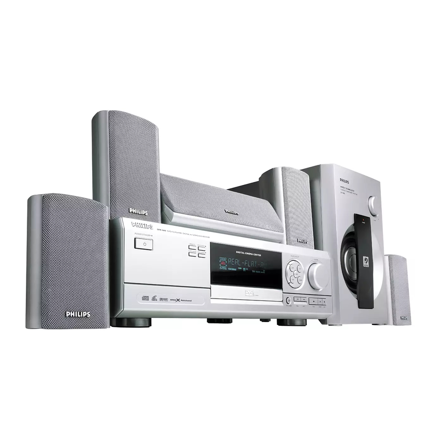
DVD Surround Receiver
Service
Service
Service
Service Manual
For Repair infromation on the Sub-woofer please refer to
Type/version package on page 1-2
©
Copyright 2001 Philips Consumer Electronics B.V. Eindhoven, The Netherlands
All rights reserved. No part of this publication may be reproduced, stored in a retrieval system or
transmitted, in any form or by any means, electronic, mechanical, photocopying, or otherwise
without the prior permission of Philips.
Published by KC 0134 Service Audio
Version 1.0
TABLE OF CONTENTS
Location Of Pc Boards & Type/version package ......... 1-2
Technical Specifications ............................................. 1-3
Measurement setup .................................................... 1-4
Service Aids, Safety Instruction, etc. .......................... 1-5
Repair Instructions ...................................................... 2-1
Disassembly Instructions & Service positions .............. 3
Set Block & Wiring diagram ........................................... 4
Psu Board ..................................................................... 5
Front Board .................................................................... 6
Tuner Board (For Information Only) ............................... 7
Av Output Board ......................................................... 8B
Dvd Module (For Information Only) ............................... 9
Audio Switch Board ..................................................... 10
Video Switch Board ..................................................... 11
Power Amplifier Board ................................................. 12
Pro-Logic Board: .......................................................... 13
Set Mechanical Exploded view & parts list ................. 14
Printed in The Netherlands
Subject to modification
MX1050D/
MX1060D/
Page
CLASS 1
LASER PRODUCT
GB
22
22S
3139 785 22950
Advertisement
Table of Contents

Related Manuals for Philips MX1060D


Summary of Contents for Philips MX1060D
- Page 1 LASER PRODUCT © Copyright 2001 Philips Consumer Electronics B.V. Eindhoven, The Netherlands All rights reserved. No part of this publication may be reproduced, stored in a retrieval system or transmitted, in any form or by any means, electronic, mechanical, photocopying, or otherwise without the prior permission of Philips.
-
Page 2: Psu Board
Pro-Logic AV Output Board Board Board Board Board VERSION PACKAGE: Type /Versions: MX1050D MX1060D For repair see Service Manual with 12NC given below Package Unit: /22S Center Unit DFR1500/00 Center Unit DFR1600/00S Sub-woofer SW965/00 3139 785 22970 Sub-woofer SW966/00S 3139 785 22890... - Page 3 Mains voltage : 230V NTSC Test Disc : ABEX - TDV540 Mains frequency : 50Hz PAL Test Disc : PHILIPS - LVP10.01 Power consumption : < 4W at Standby : 75 Ω Load Impedance < 450W Maximum : 650 ± 5nm...
- Page 4 S-Video/Scart/Digital Output Tuner AM Band LOAD SCOPE SSG=Standard Signal Generator 8 OHM 2 CH SCOPE AC LEVEL SCOPE 2 CH METER LOOP AM LOOP AM/FM SSG AC LEVEL METER AC METER LEVEL 2 CH AC LEVEL 2 CH METER DISTORTION METER 2 CH COAX...
- Page 5 SERVICE AIDS Service Tools: Universal Torx driver holder ........4822 395 91019 Complete kit ESD3 Torx bit T10 150mm ..........4822 395 50456 (combining all above products) ......4822 320 10671 Torx driver set T6 - T20 ......... 4822 395 50145 Wristband tester ............
- Page 6 WAARSCHUWING WARNING Alle IC’s en vele andere halfgeleiders zijn All ICs and many other semi-conductors are gevoelig voor electrostatische ontladingen susceptible to electrostatic discharges (ESD). (ESD). Careless handling during repair can reduce life Onzorgvuldig behandelen tijdens reparatie kan drastically. de levensduur drastisch doen verminderen. When repairing, make sure that you are Zorg ervoor dat u tijdens reparatie via een connected with the same potential as the mass...
- Page 7 MX10xxD REPAIR CHART MX10xxD Repair Chart Main Unit Audio output No sound All channel no sound Tuner no DVD Audio output no output Re-insert and fix the Check all cable is loose Video output No sound & Audio output cable Check Prologic BD or bad INT No picture...
- Page 8 MX10xxD REPAIR CHART Video Output No signal No Sound & picture C-Video no output S-Video (UL) SCART Video (CE) no output Check Audio BD CBL13A Check Prologic BD. Video BD Pin4=+12V Audio BD power supply. test PSU Pin6=-12V BD CBL02A +/-12VDC, +5V Check Video Pin7=+5V BD power supply UV3...
- Page 9 MX10xxD REPAIR CHART - DVD SECTION MX10xxD Repair Chart DVD Section Cannot read Video output DVD no Tray cannot Mechanical No sound & No Sound No Sound DVD Main Board Connector Data Noise Disc or No Signal picture Function Analog no output Digital no output opern Intermittent...
- Page 10 MX10xxD REPAIR CHART - DVD SECTION DVD no function No Sound Analog no output No Sound Digital no output Check DVD BD power Check PSU BD CBL03A Check Front BD supply JP1 connector DATA connector pin7 DVD CPU U5/pin2 One of the channel All channel (see page 10-3) power=4.8VDC...
- Page 11 ADDITIONAL INFORMATION FOR DVD SECTION 1. Clock Check 3. DVD Interface 4. Audio LR - Clock Switch Check Clock name Test point Frequency Figure Remarks Test name Test point Figure Remarks Clock Frequency Test point Remarks XERROR/P-START Pin 39 (ICS1) High/Low 27MHz Pin 118 (ICS1)
- Page 12 ADDITIONAL INFORMATION FOR DVD SECTION Figure 7-c Figure 5-e Figure 6-b Figure 7-f 7. Video Output Check Playback TDV540 Color Bar Test name Test point Condition Figure RED OUT conn. HS6-RED PLAY 8. Tray Open / Close - driver LB1641 output GREEN OUT conn.
- Page 13 DISMANTLING INSTRUCTIONS Dismantling of the Front Panel Assembly Dismantling of the DVD Module and/or Digital Board 1) Open the DVD Tray by using the Open/Close Button while 2) Return the set to its upright position and remove the Tray 1) Loosen 10 screws A to remove the DVD Digital Board Note: - Care should be taken not to entangle / damage the Set is ON and disconnect the mains supply after Cover as shown in Figure 1 and close the tray manually by...
- Page 14 Dismantling the Tuner, Audio Switch, Video Switch, Pro-Logic and AV Board (Refer figure 8) 1) Loosen 2 screws E on the Rear panel to remove the Tuner 4) Loosen 3 screws H to remove the Pro-Logic Board. Board. - 2 screws on the Rear panel - 1 screw (including metal mounting bracket) on the 2) Loosen 2 screws F on the Rear panel to remove the Audio inside of the set as shown in figure 5.
- Page 15 SERVICE POSITIONS & REPAIR HINTS SERVICE POSITIONS & REPAIR HINTS Service pos A Service pos C Paper Note: In some service positions the components or copper patterns of one board may risk touching its neigh- bouring pc boards or metallic parts. To prevent such short-circuit use a piece of hard paper or other insulating material between them.
- Page 16 SET BLOCK DIAGRAM MX10... Block Diagram dd wk124-4...
- Page 17 SET WIRING DIAGRAM...
- Page 18 PQ12CG3032F Internal Block PQ12CG3032F Voltage On/Off Regulator Circuit 5 ON/OFF PWM Comp Soft COM 3 PSU BOARD Start Overcurrent Detection Cricuit Oscillator Error Amp. Vref Overheat Detection Circuit TABLE OF CONTENTS PQ12CG3032F & PQ3RD13 Internal Block ....5-1 Components Layout + Voltages ........5-2 Circuit Diagram ..............
- Page 19 COMPONENTS LAYOUT CBL1 A3 CBL2 A2 CBL21 A4 RLY1 B1 CBL3 A5 C5 wire line CON4 POWER AMP BD A4 wire line AC voltages across transformer winding: Pin No. Pin No. 5 - 7 8,9V 4 - 6 8 - 10 7 - 9 11 - 13 Pin No.
- Page 20 CIRCUIT DIAGRAM Replace by wire Replace by wire CBL1 B6 CBL2 D6 CBL21 C6 CBL3 A6 CON4 D2 RLY1 B2...
- Page 21 ELECTRICAL PARTS LIST -- PSU BOARD MISCELLANEOUS 9965 000 09695 SOCKET 2-PIN 10MM A2361WV2-2P 9965 000 10628 CAP ELEC 220UF 16V 20% 105°C 4822 070 36302 FUSE T6,3A 250V 9965 000 10628 CAP ELEC 220UF 16V 20% 105°C 4822 070 32002 FUSE T2A 250V RESISTORS 4822 070 32002...
- Page 22 FTD DISPLAY PIN ASSIGNMENT & CONNECTION FRONT BOARD Col 1 Col 2 (11G) (2G - 10G) TABLE OF CONTENTS Col 1 FTD Display pins connection ........... 6-1 Col 2 Components Layout + Voltages ........6-2 UPD780024GC Internal Block ......... 6-3 M74HC138 &...
- Page 23 LAYOUT DIAGRAM CBL04 A7 VFD1 A4 CBL05 A8 CBL09 C1 CON17 B4 SW10 B7 CONA A9 R111 SW12 B8 R112 SW13 A7 SW14 C9 SW15 C9 SW16 C8 SW17 C7 SW18 C8 SW19 C7 CBL03 A2 VFD1 U1 (UPD16315) U2 (74HC138B) U3 (XL24C04) U5 (D78F0034) Pin No.
- Page 24 UPD780024GC INTERNAL BLOCK 64 63 62 61 60 59 58 57 56 55 54 53 52 51 50 49 P50/A8 P71/TI01 P51/A9 P70/TI00/TO0 P52/A10 P03/INTP3/ADTRG P53/A11 P02/INTP2 P54/A12 P01/INTP1 P55/A13 P00/INTP0 P56/A14 P57/A15 RESET P10/ANI0 17 18 19 20 21 22 23 24 25 26 27 28 29 30 31 32 TI00/TO0/P70 16-bit timer/ Port 0...
- Page 25 M74HC138 INTERNAL BLOCK & TRUTH TABLE TRUTH TABLE INPUTS OUTPUTS ENABLE SELECT & X = Don't care UPD16315 INTERNAL BLOCK uPD16315 Dimming circuit Command decoder Display memory Serial 24 buts x 12 words Interface /Grid Timing generator key scan /Grid Key data memory(2x16 bits) Grid 10, 11...
- Page 26 CIRCUIT DIAGRAM CBL03 B3 CBL04 A1 CBL05 B1 CBL09 C1 CON17 A4 CONA B1 SW10 D4 SW12 D4 SW13 D4 SW14 C4 SW15 C4 SW16 C4 SW17 C4 SW18 C4 SW19 C4 VFD1 A5 R111 R112...
- Page 27 ELECTRICAL PARTS LIST - FRONT BOARD ELECTRICAL PARTS LIST - FRONT BOARD MISCELLANEOUS SW1 9965 000 10149 SW TACT 1P1T 20MA 15V H=5MM 9965 000 09681 RES CF 560 OHM 5% 1/6W AXIAL 9965 000 09674 RES CF 10K OHM 5% 1/6W AXIAL 9965 000 10117 TR SS9014 NPN HFE 200 270MHZ 9965 000 10134...
-
Page 28: Tuner Board (For Information Only)
TUNER BOARD (For Information Only) It is not recommended for component repair on this board but to replace the board when it becomes defec- tive. Therefore no service parts list are published in this Chapter. The service parts available for replacement are: Tuner Board .......... - Page 29 TUNER CIRCUIT...
- Page 30 8B-1 8B-1 Technical Notes: AV OUTPUT BOARD (SCART version) TABLE OF CONTENTS Components & Chips Layout ......... 8B-2 Circuit Diagram .............. 8B-3 Electrical parts list ............8B-4...
- Page 31 8B-2 8B-2 COMPONENTS LAYOUT CHIPS LAYOUT SKY MOUNT CN13 RA22 RN17 RN28 CA16 CN14 RA23 RN18 RN29 CA17 CN15 RA61 RN19 RV10 CA74 CN16 RN30 CB15 CN17 RN10 RN20 RN31 CB16 CN18 RN11 RN22 RN32 CBL21B B3 CN19 RN12 RN23 RN33 CV10 RN13...
- Page 32 8B-3 8B-3 CIRCUIT DIAGRAM RN28 CA16 RN29 CA17 CA74 RN30 CB15 RN31 CB16 RN32 CBL21B A5 RN33 CN10 CN11 CN12 CN13 CN14 CN15 RV10 CN16 CN17 CN18 CN19 CN20 CN21 CN22 CV10 CV12 CV13 RA17 RA22 RA23 RA61 RN10 RN11 RN12 RN13 RN14...
- Page 33 8B-4 8B-4 ELECTRICAL PARTS LIST - AV (SCART) OUTPUT BOARD ELECTRICAL PARTS LIST - AV (SCART) OUTPUT BOARD MISCELLANEOUS 4822 130 10845 GP1F32T 4822 117 11927 75R 1% 0,1W 4822 130 83338 LL4148 4822 117 11454 820R 1% 0,1W 9965 000 10073 RCA SOCKET 1P BLACK RN10 4822 051 20129 12R00 5% 0,1W...
- Page 34 Europe The Circuit & Layout diagrams are published for refer- MX1055D/37S ence only. The repair assistance on DVD section is MX1060D/22S Europe given on Chapter 2. * Note: The Region code may differs in some countries, in such case the Region code of the country should be used.
- Page 35 DVD MAIN BOARD - TOP VIEW DVD MAIN BOARD - BOTTOM VIEW...
- Page 36 DVD CIRCUIT 1...
- Page 37 DVD CIRCUIT 2...
- Page 38 DVD CIRCUIT 3...
- Page 39 DVD CIRCUIT 4...
-
Page 40: Audio Switch Board
10-1 10-1 LC78212 Internal Block LC78212 L1 1 30 R1 L2 2 29 R2 L3 3 28 R3 AUDIO SWITCH BOARD 27 RCOM1 LCOM1 4 L4 5 26 R4 L5 6 25 R5 L6 7 24 R6 23 RCOM2 LCOM2 8 TABLE OF CONTENTS IN7 9 22 R7... - Page 41 10-2 10-2 COMPONENTS LAYOUT CHIPS LAYOUT sky mount CA17 B4 CA28 A2 RA17 B4 sky mount CA18 B4 CA29 A2 RA18 C3 sky mount CA19 B4 RA19 C3 sky mount CA30 A3 CA20 C4 CA31 A3 RA20 C3 CA10 A3 CA21 C4 CA32 A3 CBL12 C2...
- Page 42 10-3 10-3 CIRCUIT DIAGRAM CA10 B5 CA11 B6 CA12 B5 CA13 B6 CA14 B6 CA15 B6 CA16 B6 CA17 C5 CA18 C6 CA19 C5 CA20 C4 CA21 C4 CA22 A2 CA23 C2 CA24 C2 CA25 D2 CA26 D3 CA27 A3 CA28 A3 CA29 A4 CA30 A4...
- Page 43 10-4 10-4 ELECTRICAL PARTS LIST - AUDIO SWITCH BOARD MISCELLANEOUS 4822 051 20474 470K 5% 0,1W 9965 000 09656 RCA SOCKET 4P RED/WHITE 4822 117 11139 1,5K 1% 0,1W 9965 000 09656 RCA SOCKET 4P RED/WHITE 4822 051 20474 470K 5% 0,1W 4822 117 11139 1,5K 1% 0,1W CAPACITORS...
-
Page 44: Video Switch Board
11-1 11-1 LC7824 Internal Block LC7824 16 COM3 IN1 1 15 IN6 14 COM2 IN2 2 13 IN5 IN3 3 VIDEO SWITCH BOARD 12 IN4 COM1 4 Level Shift VEE 5 Latch 11 VDD CE 6 Shift Register DI 7 Control 10 S TABLE OF CONTENTS... - Page 45 11-2 11-2 COMPONENTS LAYOUT CHIPS LAYOUT SKY MOUNT CV11 CV17 CV25 RV14 SKY MOUNT CV12 CV18 CV26 RV15 RV20 CBL13B A4 CV13 CV27 RV10 RV16 RV21 CBL16B B4 CV14 CV22 CV28 RV11 RV17 CV15 CV23 CV29 RV12 RV18 CV10 CV16 CV24 RV13 RV19...
- Page 46 11-3 11-3 CIRCUIT DIAGRAM CBL13B A1 CBL16B B1 CV10 CV11 CV12 CV13 CV14 CV15 CV16 CV17 CV18 CV22 CV23 CV24 CV25 CV26 CV27 CV28 CV29 RV10 RV11 RV12 RV13 RV14 RV15 RV16 RV17 RV18 RV19 RV20 RV21...
- Page 47 11-4 11-4 ELECTRICAL PARTS LIST - VIDEO SWITCH BOARD MISCELLANEOUS J1+J2 9965 000 10155 RCA SOCKET 3P YELLOW RV21 9965 000 10156 RES SMD 12K OHM 5% 1/10W 0805 9965 000 10154 RCA SOCKET 2P TRANSISTORS & INTEGRATED CIRCUITS 9965 000 10110 TR SMD T2907A HFE300 200MHZ CAPACITORS 9965 000 09652...
-
Page 48: Power Amplifier Board
12-1 12-1 LM3886 INTERNAL BLOCK LM3886 POWER AMPLIFIER BOARD OUTPUT MUTE TABLE OF CONTENTS LM3886 & UPC1237 Internal Block ......12-1 Components Layout + Voltages ........12-2 Circuit Diagram .............. 12-3 Electrical parts list ............12-4 uPC1237 INTERNAL BLOCK uPC1237 Vcc ON Overload detector mute... - Page 49 12-2 12-2 COMPONENT LAYOUT CBL06B A7 CBL17B A7 J125 Pin No. Pin No. LM3886 LM3886 LM3886 LM3886 LM3886 UPC1237 -35,5V 10,4mV 8,1mV 40mV 60mV 40mV 30mV 30mV 7,8mV -35V 14,2mV -35V -35V -35V -35V -35V 1,5V Measurement in DVD playing Mode (5,1 Channel Disc) 26mV 26mV...
- Page 50 12-3 12-3 CIRCUIT DIAGRAM CBL17 B6 CBL6...
- Page 51 12-4 12-4 ELECTRICAL PARTS LIST - POWER AMPLIFIER BOARD ELECTRICAL PARTS LIST - POWER AMPLIFIER BOARD MISCELLANEOUS 9965 000 10093 CAP ELEC GS 47UF 50V 20% 9965 000 10101 RES CF 68K OHM 5% 1/6W AXIAL 9965 000 10084 BRIDGE RECT MB252 25A 200V 9965 000 10089 CAP ELEC GR 100UF 50V 20% 9965 000 09673...
-
Page 52: Pro-Logic Board
13-1 13-1 M62464FP INTERNAL BLOCK DVss DELAY ECHOOUT BNR IN DO-SW DATA DBC1 LOGIC PRO-LOGIC BOARD DBC2 MICIN DBC3 10Kbit SRAM AGND PSC3 F.B. PSC6 DI-SW SWBP-SW SWVOLOUT PSC2 M62464FP SWVOLIN SW-SW PSC5 BNR-SW SWOUT PSC1 SRVOLOUT PSC4 SRVOLIN SR-SW RLC5 TABLE OF CONTENTS SROUT... - Page 53 13-2 13-2 COMPONENTS & CHIPS LAYOUT C100 C101 C102 C103 C104 C105 J100 C107 J101 C108 J102 C109 C110 C111 C112 C113 C114 C115 C116 C117 C118 C119 C120 C121 C122 C123 C124 C125 C126 C127 C128 C129 C130 C131 C132 C133 C134...
- Page 54 13-3 U3 (M62464FP) Pin No. Voltage Pin No. Voltage Pin No. Voltage Pin No. Voltage 4,33V 4,98V 4,34V 4,36V 4,33V 4,7V 4,34V 4,27V 3,52V 38,5mV 4,34V 4,36V 2,43V 38,8mV 4,34V 4,34V 4,34V 5,9mV 83mV 4,34V 4,37V 4,33V 4,34V 4,33V 4,34V 2,44V 4,05V 4,43V...
- Page 55 13-4 BA4558N INTERNAL BLOCK BA4558N – – M62420FP INTERNAL BLOCK 1.8K SIMAMP2 136K S2 S4 S6 S8 TONE AMP2 6.5K 6.5K VOLAMP2 M62420SP/FP CONTROL LOGIC VOLAMP1 6.5K 6.5K TONE AMP1 S1 S3 S5 S7 I C BUS INTER 136K SIMAMP1 FACE 1.8K...
- Page 56 13-5 13-5 CIRCUIT DIAGRAM CBL5 C100 C101 C102 C103 C104 C105 C107 C108 C109 C110 C111 C112 C113 C114 C115 C116 C117 C118 C119 C120 C121 C122 C123 C124 C125 C126 C127 C128 C129 C130 C131 C132 C133 C134 C135 C136 C137 C138...
- Page 57 13-6 13-6 ELECTRICAL PARTS LIST - PRO-LOGIC BOARD ELECTRICAL PARTS LIST - PRO-LOGIC BOARD MISCELLANEOUS RESISTORS RCAS19965 000 10073 RCA SOCKET 1P BLACK C111 9965 000 10056 CAP CER 0,22UF 25V 10% Y5V 9965 000 10074 RES SMD 10K OHM 5% 1/10W 0805 4822 117 10837 100K 1% 0,1W C112 9965 000 10056...
- Page 58 14-1 SET EXPLODED VIEW Release week 135-1 84 2X...
- Page 59 KNOB LENS TRANSPARENT 9965 000 10178 SIDE CAP LEFT ABS BLACK 9965 000 10418 SIDE CAP LEFT SILVER 9965 000 10179 LOGO BADGE PHILIPS B/BLACK 9965 000 10419 LOGO BADGE PHILIPS B/SILVER 9965 000 10180 MODE KNOB ABS BLACK 9965 000 10420...