
Related Manuals for Sangean ATS-909X


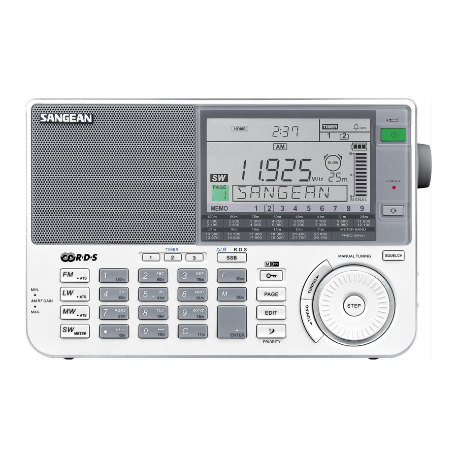
Summary of Contents for Sangean ATS-909X
-
Page 1: Table Of Contents
ATS-909X FM / MW / LW / SW PLL SYNTHESIZED RECEIVER CONTENTS Specification Main PCB Block Diagram Control PCB Block Diagram Alignment Instructions 9-16 Test Points Diagram Main PCB Top View Main PCB Bottom View Control PCB Top View Control PCB Bottom View... -
Page 2: Specification
Specification FM. ELECTRICAL PERFORMANCE R.H. Date Page rand ∘C Temp 25 Ver. ATS-909X(CE) SANGEAN 2010/12/21 Condition Value Test No. Test Item Unit Input Output freq Nom. Lim. 0.05 87.5 Tuning Range S/N=6dB 0.05 108.0 0.05 Intermediate freq. S/N=6dB 10.7 90MHz Max. - Page 3 Specification MW ELECTRICAL PERFORMANCE ∘ R.H. Date Page Temp 25 Model ;ATS-909X(CE SANGEAN Ver. rand 2010/12/21 Condition Value Test No. Test Item Unit Input Output Freq. Nom. Lim. Min. Tuning Range Max. 1710 1st IF 55845 Intermediate freq. S/N=6 dB...
- Page 4 Specification SW ELECTRICAL PERFORMANCE R.H. Date Page Temp 25 ∘ SANGEAN Mode ATS-909X(CE) Ver. rand 2010/12/21 Condition Value Test No. Test Item Unit Input Output Freq. Nom. Lim. Min. 1711 Tuning Range Max. 29999 . IF 55845 Intermediate freq. S/N=6Db .
- Page 5 Specification LW ELECTRICAL PERFORMANCE ∘ R.H. Date Page Temp 25 Model SANGEAN Ver. rand ATS-909X(CE) 2010/12/21 Condition Value Test No. Test Item Unit Input Output Freq. Nom. Lim. Min. Tuning Range Max. 1st. IF 55845 Intermediate freq. S/N=6dB 2nd. IF 180KHz Max.
- Page 6 Specification AUX-IN ELECTRICAL PERFORMANCE ∘ R.H. Date Page Temp 25 Mode SANGEAN Ver. rand ATS-909X(FCC) 2010/12/21 Condition Value Test No. Test Item Unit Input Output Freq. Nom. Lim. AUX IN=0.5V/400Hz Output Power 1500 1000 THD=10% Output=R.0 AUX IN THD=3% Dynamic Range...
-
Page 7: Main Pcb Block Diagram
MAIN PCB BLOCK DIAGRAM... -
Page 8: Control Pcb Block Diagram
CONTROL PCB BLOCK DIAGRAM... -
Page 9: Alignment Instructions
ALIGNMENT INSTRUCTIONS ALIGNMENT FOR 452KHZ / 448KHZ OSCILLATOR Required Instrument Frequency Counter Alignment Procedure Setting Procedure Connect a frequency counter to TP1. RECEIVING 15.1 MHz FREQUENCY Turn the radio to ON and set AM mode to “USB”. BAND Adjust TC1 to have a reading specification frequency 452KHz 30Hz. - Page 10 ALIGNMENT FOR AM 2ND LOCAL OSCILLATOR Required Instrument RF Signal Generator (RFSG) Frequency Counter Alignment Procedure Setting Procedure Set RFSG output level to 80 emf/dBµ and frequency to 55.845MHz RECEIVING 15.1 MHz with modulation 1KHz 30%. FREQUENCY Turn the radio to ON and set AM mode to “AM”. BAND Turn the radio receiving frequency to 15.1MHz.
- Page 11 ALIGNMENT FOR AM SENSITIVITY Required Instrument RF Signal Generator (RFSG) SSVM Alignment Procedure Setting Procedure Turn the radio to ON and tune receiving frequency to 15.1MHz. RECEIVING 15.1 MHz FREQUENCY Set RF Gain VR301 to Max. and slide Wide/Narr. switch to WIDE. BAND Feed a signal with 1KHz 30% modulation from RFSG into ANT IN AM MODE...
- Page 12 ALIGNMENT FOR 450KHz TRAP Required Instrument RF Signal Generator (RFSG) With Loop Antenna SSVM Alignment Procedure Setting Procedure Turn the radio to ON and tune receiving frequency to LW 450KHz. RECEIVING 450KHz FREQUENCY Feed a 450KHz signal with 1KHz 30% modulation to loop antenna. BAND Connect a SSVM to speaker output (TP4).
- Page 13 ALIGNMENT FOR TIME BASE OF FREQUENCY Required Instrument RF Signal Generator (RFSG) Frequency Counter Alignment Procedure Setting Procedure Connect a RFSG to ANT IN (TP2) and set frequency to 15.1MHz and RECEIVING 15.1 MHz FREQUENCY output to 40 emf/dBµ without modulation. BAND Set AM mode to LSB mode and volume turn to maximum.
- Page 14 ALIGNMENT FOR USB/LSB FINE TUNING Required Instrument RF Signal Generator (RFSG) Frequency Counter Alignment Procedure Setting Procedure Turn the radio to on and tune the receiving frequency to 15.1MHz. RECEIVING 15.1 MHz FREQUENCY Set the AM mode to “USB” mode. BAND Set the tuning step to “SLOW”.
- Page 15 ALIGNMENT FOR TIME BASE OF FREQUENCY Required Instrument RF Signal Generator (RFSG) Alignment Procedure Setting Procedure Tune the radio to ON. RECEIVING 15.1 MHz FREQUENCY Connect the RFSG to ANT IN (TP2) and set frequency to BAND 15.1MHz with 1KHz modulation. AM MODE Connect a DVM to TP6.
- Page 16 ALIGNMENT FOR AM SSB. IF SENSITIVITY Required Instrument RF Signal Generator (RFSG) SSVM Alignment Procedure Setting Procedure Turn the radio to ON and tune receiving frequency to 15.1MHz. RECEIVING 15.1 MHz FREQUENCY Set RF Gain VR301 to Max. and slide Wide/Narr. switch to WIDE. BAND Feed a signal with 1KHz 30% modulation from RFSG into ANT IN AM MODE...
-
Page 17: Test Points Diagram
TEST POINTS DIAGRAM... -
Page 18: Main Pcb Top View
MAIN PCB TOP VIEW... -
Page 19: Main Pcb Bottom View
MAIN PCB BOTTOM VIEW... -
Page 20: Control Pcb Top View
CONTROL PCB TOP VIEW... -
Page 21: Control Pcb Bottom View
CONTROL PCB BOTTOM VIEW... -
Page 22: Key Pcb Top View
KEY PCB TOP VIEW... -
Page 23: Key Pcb Bottom View
KEY PCB BOTTOM VIEW... -
Page 24: Wiring Diagram
WIRING DIAGRAM... -
Page 25: Troubleshooting Flow Chart
TROUBLESHOOTING FLOW CHART The radio power can not turn to ON Check whether clock time show on the Check the power supply of µ-com and LCD and the color is flashing. connectors. (CN302, W302) NORMAL Check X301, X302. Check whether battery mark is flashing on Check whether any key had short. - Page 26 SSB function do not work Check whether reception is normal in AM Check AM receiving circuit. mode. NORMAL Check the oscillator frequency of TP1 whether 448KHz in LSB mode or 452KHz Check the circuit of Q6, Q7 and Q8. in USB mode. Check the oscillator circuit Q9 and T2.
- Page 27 Speaker have not voice output Check whether the speaker is normal. Change the speaker. Check whether the connect wires one open from PCB to speaker. Check whether earphone action is normal Check JK5. while an earphone plug in to JK5. Check the circuit of IC6 and IC7.
- Page 28 Weak sensitivity in AM band Check whether reception is normal in Check the front end Amp Q15~Q19. MW/LW band. NORMAL Check the antenna circuit and antenna Check whether both the VCO and 2’nd switch (D1, Q1, JK1, L3 and L1). OSC are normal.
-
Page 29: Electrical Parts List
ELECTRICAL PARTS LIST ATS-909X PART NO. DESCRIPTION Q'TY REMARK 1001170 CH LSI UPD78F0513A IC 305, 1011362 CH IC XC62FP3002PRN IC 4, 1012072 CH IC NJM2100M DMP8 IC 5, 1012410 CH IC MB15A01PFV1-G-BND IC 304, 1012620 IC PHOTOCOUPLE PC-17K1 IC 8,... - Page 30 1320393 S.F-VR 10KB TB067A-0D SVR1, 1320397 S.F-VR 200KB TB067A-0D SVR2, 1601001 LCD 0121A-HTGT ATS-909X 1615481 PCB A ATS-909X 1.2T/2 PCB A 1615490 PCB C ATS-909X 1.2T/2 PCB C 1615500 PCB D ATS-909X 1.2T/2 PCB D 1620880 SPK 3" 8Ω 3W(MAX)
- Page 31 ELECTRICAL PARTS LIST ATS-909X PART NO. DESCRIPTION Q'TY REMARK 1702050 CNT BASE 2.5x4P CN 1, 1702A3D CH HOUSING 2x13P-S CN 302, 170310143010 CNT/W-A 100(2+3P) W 201, 170312154010 CNT/W-A 120(2.5+4P) W 303, 17035504C010 CNT/W-A 55(12P+12P)P=2 W 302, 17035504D010 CNT/W-A 55(2+13P) W 2,...
- Page 32 ELECTRICAL PARTS LIST ATS-909X PART NO. DESCRIPTION Q'TY REMARK 173,186,189,190,307, 341-343,346,349,350, -352,353,357,361,363 365,376,385-387,154, 5410471 CH CC 104Z 25V Y5V-C C 300,305,308-319,321, -322,325,327,328,366 368,374,382-384,32, 39,43,51,52,55,63,94 ,104,159,4,178,180,183, 5410557 CH CC 105Z 10V F-C C 7,9,12,16,76,90,158, 165,166,168,170,171, 185,197,198,132,324, 326,330,373, 5412001 CH CC 120J 50V NPO-C...
- Page 33 ELECTRICAL PARTS LIST ATS-909X PART NO. DESCRIPTION Q'TY REMARK 325,343,345,356,363, 364,372,375,409,410, 192,323,340, 61301104 CH RD 100KJ-0603 R 25,31,40,48,60,65,73 ,74,80,92,102,109, 116,121,127,146,311, 152,159,171,174,175, 249,255,263,351,352, 374,383,396,405,407,12, 61301105 CH RD 1MJ-0603 R 128,185,353,382,403, 404,406,408,137,413, 61301122 CH RD 1K2J-0603 R 89,100,107,95, 61301123 CH RD 12KJ-0603...
- Page 34 ELECTRICAL PARTS LIST ATS-909X PART NO. DESCRIPTION Q'TY REMARK 61301473 CH RD 47KJ-0603 R 29,14,67,68,147,177, 181,182,184,207,210, 253,303,304,326,327, 338,339,359-362,370, 384,411,414, 61301474 CH RD 470KJ-0603 R 11,124,160,310,357,358, 61301475 CH RD 4M7J-0603 R 222, 61301562 CH RD 5K6J-0603 R 1,187, 61301563 CH RD 56KJ-0603...
-
Page 35: Mechanical Parts List
MECHANICAL PARTS LIST ATS-909X Ref no PART NO. DESCRIPTION Q'TY APP./DWG NO. REMARK 2000TW00000 FUNCTION HOLDER A3-TW-01 2000TW00100 LCD LIGHT LENS A3-TW-02 21004100600 SHI DC/DC-DOWN A4-202-1737 21005900100 DC/DC SHIELD (UP) A4-800-1217 21008600700 VCO SHIELD (UP) A4-909-2114 2100M40060B BATTERY CONTACT ASS'Y+... -
Page 36: Mechanical Parts List
3107TW0000010 TIME SET KEY A3-TW-17 3108TW0000010 STEP KNOB A3-TW-18 3109TW0000010 AUX IN KNOB A3-TW-19 310ATW0000010 LIGHT KEY A3-TW-21 310BTW0000010 FUNCTION KAY ASS' A3-TW-22 3120TW0000010 BATTERY COVER A3-TW-08 3150TW0000010 REAR PLATE A3-TW-24 3230TW0000010 SPK GRILL A3-TW-26 3270TW0000010 ROD ANT 3A74TW0000100 SANGEAN BADGE... -
Page 38: Ic Circuit Block Diagram
IC CIRCUIT BLOCK DIAGRAM Si4735-D60 UTC7640P... - Page 39 TC4066BFN XC62FP3002PRN...
- Page 40 NJM2100M PT2308...
- Page 41 NJM2073D PC-17K1...
- Page 42 MC33340 10. IC10 LD1117AL-ADJ...
- Page 43 11. IC300 24LC32A 12. IC304 MB15A01PFV1...
- Page 44 13. IC305 UPD78F0513A 14. IC306 XC6202P302PRN...
-
Page 45: Semiconductor Lead Identifications
SEMUCONDUCTOR LEAD IDENTIFICATIONS Transistors (TOP VIEW) (TOP VIEW) 2SA812 2SA1020 2SK433B 2SK715W 2SB815 2SK2880A 2SC1623 2SC2223 2SC4154 2SD1048 (E: Emitter C: Collector B: Base S: Source G: Gate D: Drain) Diodes 1N4002 SVC201SPA W04M 1.5A ZENER 3V 1N5817 ZENER RD5V1 1N60P ZENER 6V8 ZENER RD15... -
Page 46: Ic And Transistor Voltage Chart
IC AND TRANSISTOR VOLTAGE CHART Si4735-D60 UTC7640P TC4066BFN FM MW LW SW AUX FM MW LW SW AUX FM MW LW SW AUX 0.56 0.54 0.54 0.54 0.54 1.52 1.48 1.5 1.51 1.48 1.5 0.3 0.26 0.15 0.06 0.08 2.24 2.2 0.3 0.22 0.13 0.05 0.07 0.46 0.44 0.44 2.24 2.2... - Page 47 PC-17K1 MC33340 IC300 24LC32A FM MW LW SW AUX FM MW LW SW AUX FM MW LW SW AUX 8.85 8.85 8.85 8.85 8.85 2.77 2.77 2.77 2.77 2.77 IC10 LD1117AL-ADJ 2.77 2.77 2.77 2.77 2.77 FM MW LW SW AUX 2.73 2.73 2.73 2.73 2.73 IC301 AP650...
- Page 48 IC302 AP650 FM MW LW SW AUX PIN FM MW LW SW AUX PIN FM MW LW SW AUX 1.37 1.37 1.37 1.37 1.37 1.39 1.37 1.37 1.37 1.37 44 1.35 1.35 1.35 1.35 1.35 1.39 1.37 1.37 1.37 1.37 45 1.35 1.35 1.35 1.35 1.35 1.37 1.37 1.37 1.37 1.37 46 1.35 1.35 1.35 1.35 1.35...
- Page 49 IC305 UPD78F0513A SW AUX PIN SW AUX PIN SW AUX 2.78 2.78 2.78 2.78 2.77 2.78 2.78 2.78 2.78 2.77 2.77 2.84 2.84 2.84 3.16 3.18 3.18 3.18 3.18 2.79 2.37 2.77 2.37 2.79 2.62 2.77 2.42 2.56 2.56 1.48 1.61 1.61 1.61 1.61 2.72 2.79 2.79 0.24 0.24 0.24 0.35 0.32 0.76 0.77 0.77 0.77 0.77...
- Page 50 Transistor 0.69 0.69 0.43 5.19 5.19 6.13 6.13 6.11 0.36 0.36 0.61 0.58 0.58 0.69 0.61 6.08 6.12 6.12 6.14 0.68 0.68 0.13 6.04 6.04 0.47 0.47 0.28 0.22 0.73 0.73 0.56 0.22 1.23 1.23 1.29 5.32 5.32 5.25 0.22 2.72 2.72 2.74...
- Page 51 Transistor 0.46 0.47 0.46 0.92 0.92 0.92 Q301 0.25 0.25 0.25 7.76 7.78 7.76 0.65 0.65 0.65 0.65 0.65 2.63 2.63 Q302 2.58 2.76 2.76 2.76 2.58 8.47 9.21 9.21 8.42 8.47 9.27 9.27 9.17 9.46 9.46 9.13 9.17 Q303 9.25 9.25 9.13...
-
Page 52: Main Schematic Diagram
MAIN SCHEMATIC DIAGRAM... -
Page 53: Control Schematic Diagram
CONTROL SCHEMATIC DIAGRAM...