Sony MDS-JE330 Service Manual
Minidisc deck
Hide thumbs
Also See for MDS-JE330:
- Operating instructions manual (46 pages) ,
- Limited warranty (1 page)
Table of Contents
Advertisement
Advertisement
Table of Contents

Related Manuals for Sony MDS-JE330


Summary of Contents for Sony MDS-JE330
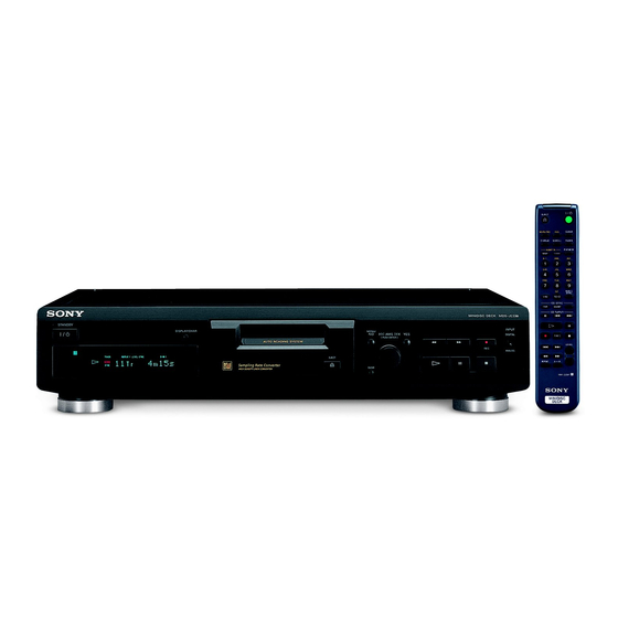
- Page 1 MDS-JE330 SERVICE MANUAL US Model Canadian Model AEP Model UK Model E Model Australian Model Model Name Using Similar Mechanism MDS-JE520 MD Mechanism Type MDM-5A Optical Pick-up Type KMS-260A/J1N SPECIFICATIONS — Continued on next page — MINIDISC DECK MICROFILM – 1 –...
- Page 2 SELF-DIAGNOSIS FUNCTION The self-diagnosis function consists of error codes for customers which are displayed automatically when errors occur, and error codes which show the error history in the test mode during servicing. For details on how to view error codes for the customer, refer to the following box in the instruction manual.
- Page 3 ITEMS OF ERROR HISTORY MODE ITEMS AND CONTENTS Selecting the Test Mode Display Details of History Displays the recording time. total rec Displayed as “rππππππh”. The displayed time is the total time the laser is set to the high power state. This is about 1/4 of the actual recording time.
- Page 4 REPLACE THESE COMPONENTS WITH SONY PARTS FONCTIONNEMENT. NE REMPLACER CES COMPOSANTS WHOSE PART NUMBERS APPEAR AS SHOWN IN THIS QUE PAR DES PIÈCES SONY DONT LES NUMÉROS MANUAL OR IN SUPPLEMENTS PUBLISHED BY SONY. SONT DONNÉS DANS CE MANUEL OU DANS LES SUPPLÉMENTS PUBLIÉS PAR SONY.
-
Page 5: Table Of Contents
SAFETY CHECK-OUT TABLE OF CONTENTS After correcting the original service problem, perform the follow- 1. SERVICING NOTE ............6 ing safety checks before releasing the set to the customer: Check the antenna terminals, metal trim, “metallized” knobs, screws, 2. GENERAL ................ -
Page 6: Servicing Note
SECTION 1 SERVICING NOTE JIG FOR CHECKING BD BOARD WAVEFORM The special jig (J-2501-149-A) is useful for checking the waveform of the BD board. The names of terminals and the checking items to be performed are shown as follows. GND : Ground I+3V : For measuring IOP (Check the deterioration of the optical pick-up laser) IOP : For measuring IOP (Check the deterioration of the optical pick-up laser) TEO : TRK error signal (Traverse adjustment) - Page 7 IOP DATA RECORDING AND DISPLAY WHEN OPTICAL PICK-UP AND NON-VOLATILE MEMORY (IC171 OF BD BOARD) ARE REPLACED The IOP value labeled on the optical pick-up can be recorded in the non-volatile memory. By recording the value, it will eliminate the need to look at the value on the label of the optical pick-up.
- Page 8 CHECKS PRIOR TO PARTS REPLACEMENT AND ADJUSTMENTS Before performing repairs, perform the following checks to determine the faulty locations up to a certain extent. Details of the procedures are described in “5 Electrical Adjustments”. Criteria for Determination Measure if unsatisfactory: (Unsatisfactory if specified value is not satisfied) Laser power check •...
- Page 9 RETRY CAUSE DISPLAY MODE • In this test mode, the causes for retry of the unit during recording can be displayed on the fluorescent indicator tube. During playback, the “track mode” for obtaining track information will be set. This is useful for locating the faulty part of the unit. •...
- Page 10 Reading the Track Mode Display Higher Bits Lower Bits Details Hexa- Hexadecimal decimal b7 b6 b5 b4 b3 b2 b1 b0 When 0 When 1 Binary Emphasis ON Emphasis OFF Stereo Monaural This is 2-bit display. Normally 01. 01:Normal audio. Others:Invalid Invalid Audio (Normal) Digital copy...
-
Page 11: General
SECTION 2 GENERAL Front Panel LOCATION OF PARTS AND CONTROLS 1 STANDBY indicator 2 1/u (Power) button 3 PLAY MODE button 4 REPEAT button 5 LEVEL/DISPLAY/CHAR button 6 DISK compartment 7 MENU/NO button 8 YES button 9 0 button 10 ) button 11 r REC (Recording) button 12 INPUT DIGITAL/ANALOG switch 13 p (stop) button... -
Page 12: Disassembly
SECTION 3 DISASSEMBLY Note: Follow the disassembly procedure in the numerical order given. 3-1. CASE AND FRONT PANEL 3 Case 2 Two screws (Case) 1 Two screws (Case) 4 Flat type wire (CN421) 6 Front panel assembly 5 Five screws (BVTP3x8) 3-2. -
Page 13: Base Unit (Mbu-5A) And Bd Board
3-3. BASE UNIT (MBU-5A) AND BD BOARD 2 Base unit (MBU-5A) 5 Flexible board (CN104) 6 Flexible board (CN101) 1 Three screws (BTP2.6x6) 3 Remove the solder (Five portion) 7 BD board 4 Screw (M1.7x4) 3-4. SW BOARD AND LOADING MOTOR (M103) 1 Screw (PTPWH M2.6x6) 2 Gear B 3 Two screws... -
Page 14: Test Mode
SECTION 4 TEST MODE 4-1. PRECAUTIONS FOR USE OF TEST MODE • As loading related operations will be performed regardless of the test mode operations being performed, be sure to check that the disc is stopped before setting and removing it. Even if the §EJECT button is pressed while the disc is rotating during continuous playback, continuous recording, etc., the disc will not stop rotating. - Page 15 4-5. SELECTING THE TEST MODE There are 24 types of test modes as shown below. The groups can be switched by rotating the AMS knob. After selecting the group to be used, press the YES button. After setting a certain group, rotating the AMS knob switches between these modes. Refer to “Group”...
- Page 16 4-5-1. Operating the Continuous Playback Mode 1. Entering the continuous playback mode 1 Set the disc in the unit. (Whichever recordable discs or discs for playback only are available.) 2 Rotate the AMS knob and display “CPLAY MODE”. 3 Press the YES button to change the display to “CPLAY MID”. 4 When access completes, the display changes to “C = AD = ”.
-
Page 17: Functions Of Other Buttons
4-6. FUNCTIONS OF OTHER BUTTONS Contents Function Sets continuous playback when pressed in the STOP state. When pressed during continuous playback, the tracking servo turns ON/OFF. Stops continuous playback and continuous recording. The sled moves to the outer circumference only when this is pressed. The sled moves to the inner circumference only when this is pressed. - Page 18 MEANINGS OF OTHER DISPLAYS Contents Display When Lit When Off During continuous playback (CLV: ON) STOP (CLV: OFF) Tracking servo OFF Tracking servo ON Recording mode ON Recording mode OFF CLV low speed mode CLV normal mode SYNC ABCD adjustment completed L.SYNC Tracking offset cancel ON OVER...
-
Page 19: Electrical Adjustments
SECTION 5 ELECTRICAL ADJUSTMENTS 5-1. PARTS REPLACEMENT AND ADJUSTMENT • Check and adjust the MDM and MBU as follows. The procedure changes according to the part replaced • Abbreviation : Optical pick-up OWH: Overwrite head • Temperature compensation offset check •... - Page 20 5-2. PRECAUTIONS FOR CHECKING LASER DIODE 4) Use the following tools and measuring devices. • Check Disc (MD) TDYS-1 EMISSINON (Parts No. 4-963-646-01) To check the emission of the laser diode during adjustments, never • Test Disk (MDW-74/AU-1) (Parts No. 8-892-341-41) view directly from the top as this may lose your eye-sight.
- Page 21 5-6. CHECKS PRIOR TO REPAIRS Note 1: After step 4, each time the YES button is pressed, the display will be switched between “ 0.7 mW *** $ ”, “ These checks are performed before replacing parts according to 6.2 mW *** $ *** $ ”, and “...
- Page 22 10. Observe the waveform of the oscilloscope, and check that the 5-6-4. Focus Bias Check specified value is satisfied. Do not rotate the AMS knob. Change the focus bias and check the focus tolerance amount. Checking Procedure : (Traverse Waveform) 1.
- Page 23 5-7. INITIAL SETTING OF ADJUSTMENT VALUE 5-9. TEMPERATURE COMPENSATION OFFSET ADJUTMENT Note: Save the temperature data at that time in the non-volatile memory Mode which sets the adjustment results recorded in the non-volatile as 25 ˚C reference data. memory to the initial setting value. However the results of the Note : temperature compensation offset adjustment will not change to the 1.
- Page 24 7. Then, rotate the AMS knob and display “LDPWR CHECK”. 5-11. TRAVERSE ADJUSTMENT 8. Press the YES button once and display “0.9 mW *** $ ”. Connection : Check that the reading of the laser power meter become 0.85 to Oscilloscope 0.91 mW.
- Page 25 5-12. FOCUS BIAS ADJUSTMENT 11. Rotate the AMS knob until the waveform of the oscilloscope moves closer to the specified value. Adjusting Procedure : In this adjustment, waveform varies at intervals of approx. 2%. 1. Load a test disk (MDW-74/AU-1). Adjust the waveform so that the specified value is satisfied as 2.
- Page 26 5-13. ERROR RATE CHECK 5-15. AUTO GAIN CONTROL OUTPUT LEVEL 5-13-1. CD Error Rate Check ADJUSTMENT Checking Procedure : Be sure to perform this adjustment when the pickup is replaced. 1. Load a check disc (MD) TDYS-1. If the adjustment results becomes “Adjust NG!”, the pickup may be 2.
- Page 27 5-15. ADJUSTING POINTS AND CONNECTING POINTS [BD BOARD] (SIDE A) CN101 D101 CN110 I+3V NOTE IC171 [BD BOARD] (SIDE B) IC101 IC121 IC192 NOTE:It is useful to use the jig. for checking the waveform. (Refer to Servicing Note on page 6.) –...
-
Page 28: Diagrams
SECTION 6 DIAGRAMS 6-1. CIRCUIT BOARDS LOCATION SW board VOL SEL board (SP) BD board MAIN board DISPLAY board KEY SW board – 28 –... -
Page 29: Block Diagrams
MDS-JE330 DIGITAL SERVO SIGNAL PROCESSOR, DIGITAL SIGNAL PROCESSOR 6-2. BLOCK DIAGRAMS EFM/ACIRC ENCODER/DECODER, SHOCK-PROOF MEMORY CONTROLLER, ATRAC ENCODER/DECODER – BD SECTION – IC121 OVER WRITE HEAD DRIVE IC181 SCTX XINIT HR901 OVER WRITE • DIN0 HEAD DIN0 • R-ch is omitted. -
Page 30: Main Section
MDS-JE330 – MAIN SECTION – IC601 OPT IN 1 A/D,D/A CONVERTER IC611 IC301 J101 OPT IN 2 IC601 DATAO VINL1 DIGITAL DIN0 IC621 OPTICAL R-CH LINE AMP J101 VINR1 R-CH DIN1 IC381, 386 OPT OUT LINE (ANALOG) DOUT IC661 VOUTL... - Page 31 MDS-JE330 WAVEFORMS THIS NOTE IS COMMON FOR PRINTED WIRING – BD (1/2) SECTION – – MAIN SECTION – BOARDS AND SCHEMATIC DIAGRAMS. (In addition to this, the necessary note is printed in each block.) 0.46Vp-p 3.2Vp-p For schematic diagrams. Note: 10MHz •...
-
Page 32: Printed Wiring Board - Bd Section
MDS-JE330 6-3. PRINTED WIRING BOARD – BD SECTION – • See page 28 for Circuit Boards Location. (Page 45) (Page 45) • Semiconductor • Semiconductor Location Location Ref. No. Location Ref. No. Location D101 D181 IC101 D183 IC121 IC124 IC103... -
Page 33: Schematic Diagram - Bd Section - (1/2)
MDS-JE330 6-4. SCHEMATIC DIAGRAM – BD (1/2) SECTION – • See page 34 for Waveforms. • See page 52 for IC Block Diagrams. • See page 55 for IC Pin Functions. (Page 39) (Page 39) (Page 40) (Page 40) (Page 40) -
Page 34: Schematic Diagram - Bd Section - (2/2)
MDS-JE330 6-5. SCHEMATIC DIAGRAM – BD (2/2) SECTION – • See page 34 for Waveforms. • See page 35 for Printed Wiring Board. (Page 37) (Page 37) (Page 38) (Page 38) (Page 37) (Page 38) (Page 38) (Page 41) (Page 41) BA033FP-E2 –... -
Page 35: Schematic Diagram - Main Section - (1/2)
MDS-JE330 6-6. SCHEMATIC DIAGRAM – MAIN (1/2) SECTION – • See page 34 for Waveforms. • See page 45 for Printed Wiring Board. • See page 59 for IC Pin Functions. (Page (Page (Page (Page 43) (Page 43) (Page 43) -
Page 36: Schematic Diagram - Main Section - (2/2)
MDS-JE330 6-7. SCHEMATIC DIAGRAM – MAIN (2/2) SECTION – • See page 34 for Waveforms. • See page 54 for IC Block Diagrams. (Page 41) (Page 42) (Page 41) (Page 41) (Page 41. 42) (Page 42) (Page – 43 –... -
Page 37: Printed Wiring Board - Main Section
MDS-JE330 6-8. PRINTED WIRING BOARD – MAIN SECTION – • See page 28 for Circuit Boards Location. (Page 48) (Page 51) (Page 36) (Page 36) • Semiconductor Location Ref. No. Location Ref. No. Location D390 D391 IC301 D401 D-10 IC351... -
Page 38: Printed Wiring Board - Panel Section
MDS-JE330 6-9. PRINTED WIRING BOARD – PANEL SECTION – • See page 28 for Circuit Boards Location. • Semiconductor Location Ref. No. Location D751 IC761 IC781 Q751 Q767 (Page 45) – 47 – – 48 –... -
Page 39: Schematic Diagram - Panel Section
MDS-JE330 6-10. SCHEMATIC DIAGRAM – PANEL SECTION – • See page 34 for Waveforms. (Page – 49 – – 50 –... -
Page 40: Schematic Diagram - Bd Switch Section
MDS-JE330 6-13. IC BLOCK DIAGRAMS 6-11. SCHEMATIC DIAGRAM – BD SWITCH SECTION – – BD Section – IC101 CXA2523AR 43 42 USROP – RF AGC – USRC RFA1 (Page 41) BPF3T RFA2 PEAK3T – HLPT –1 – – –2 –... - Page 41 IC121 CXD2654R 100 99 98 97 96 95 94 93 92 91 90 89 88 87 86 85 84 83 82 81 80 79 78 77 76 SPINDLE GENERATOR SERVO 75 TE MNT0 74 SE MNT1 MONITOR EACH 73 AVSS CONTROL BLOCK MNT2...
- Page 42 • MAIN section IC301 UDA1341TS/N2 VINL2 VINR2 0DB/6DB 0DB/6DB ADC2R ADC2L VINL1 VINR1 SWITCH SWITCH ADC1L ADC1R AGCSTAT VDDD DIGITAL AGC VSSD DIGITAL MIXER DECIMATION FILTER OVERFLOW DATAO L3CLOCK DIGITAL L3-BUS L3MODE INTERFACE INTERFACE L3DATA DATAI DSP FEATURES SYSCLK PRAK INTERPOLATION FILTER QMUTE DETECTOR...
-
Page 43: Ic Pin Functions
6-14. IC PIN FUNCTIONS • IC101 RF Amplifier (CXA2523AR) (BD board) Pin No. Pin Name Function I-V converted RF signal I input I-V converted RF signal J input Middle point voltage (+1.5V) generation output 4 to 9 A to F Signal input from the optical pick-up detector Light amount monitor input Laser APC output... - Page 44 • IC121 Digital Signal Processor, Digital Servo Signal Processor, EFM/ACIRC Encoder/Decoder, Shock-proof Memory Controller, ATRAC Encoder/Decoder, 2M Bit DRAM (CXD2654R) (BD board) Pin No. Pin Name Function FOK signal output to the system control (monitor output) MNT0 (FOK) “H” is output when focus is on MNT1 (SHCK) Track jump detection signal output to the system control (monitor output) MNT2 (XBUSY)
- Page 45 Pin No. Pin Name Function Data input/output for DRAM 50, 51 D2, D3 MVCI Clock input from an external VCO (Fixed at “L”) I (S) ASYO Playback EFM duplex signal output ASYI I (A) Playback EFM comparator slice level input AVDD —...
- Page 46 Pin No. Pin Name Function Tracking servo drive PWM output (+) TFDR — +3V power supply (Digital) DVDD Focus servo drive PWM output (+) FFDR Focus servo drive PWM output (–) FRDR 176.4 kHz clock signal output (X’tal) (Not used) Sled servo drive PWM output (–) SRDR Sled servo drive PWM output (+)
- Page 47 • IC501 System Control (M30620MC-400FP) (MAIN board) Pin No. Pin Name Function Not used (Fixed at “L”) 1, 2 C1 error rate voltage output (Fixed at “L”) C1ER AD error rate voltage output (Fixed at “L”) ADER ADIP sync or subcode Q sync input from CXD2654R SQSY Remote controls A1 Control input (Fixed at “L”)
- Page 48 Pin No. Pin Name Function PB-P Detection signal input from the playback position detection switch REC/PB Not used Write: “H” +3.3V — +3.3V power supply Not used (Fixed at “L”) — Ground Data signal input/output pin with the backup memory MNT3 (SLOCK) In the state of spindle srvo lock from the CXD2564R WR PWR...
-
Page 49: Exploded Views
SECTION 7 EXPLODED VIEWS NOTE: The components identified by • Items marked “*” are not stocked since they are • Abbreviation mark ! or dotted line with mark seldom required for routine service. Some delay CND : Canadian model ! are critical for safety. should be anticipated when ordering these items. -
Page 50: Front Panel Section
4-216-346-01 BUTTON (EJECT) * 65 A-4724-615-A KEY SW BOARD, COMPLETE (SP) 4-216-345-01 BUTTON (SUB) 4-216-344-01 BUTTON (POWER) * 66 4-216-341-01 HOLDER (FL) 4-996-698-01 EMBLEM, SONY * 61 A-4724-610-A DISPLAY BOARD, COMPLETE (US,CND) FL771 1-517-865-11 INDICATOR TUBE, FLUORESCENT – 62 –... -
Page 51: Mechanism Section (Mdm-5A)
7-3. MECHANISM SECTION (MDM-5A) not supplied M103 MBU-5A Ref. No. Part No. Description Remark Ref. No. Part No. Description Remark * 201 1-671-115-21 SW BOARD 4-996-227-01 LEVER (HEAD) * 202 4-996-217-01 CHASSIS 4-996-223-11 INSULATOR (F) 4-996-229-01 SPRING (HEAD LEVER), TORSION * 204 4-996-218-01 BRACKET (GUIDE R) 4-996-212-01 LEVER (LIMITTER) -
Page 52: Base Unit Section (Mbu-5A)
7-4. BASE UNIT SECTION (MBU-5A) HR901 not supplied not supplied M101 S102 M102 Les composants identifiés par une The components identified by marque ! sont critiques pour la mark ! or dotted line with mark ! are critical for safety. sécurité. -
Page 53: Electrical Parts List
SECTION 8 ELECTRICAL PARTS LIST Note: • SEMICONDUCTORS • Due to standardization, replacements in the parts list The components identified by In each case, u: µ , for example: may be different from the parts specified in the mark ! or dotted line with mark uA...: µ... - Page 54 DISPLAY Ref. No. Part No. Description Remark Ref. No. Part No. Description Remark L121 1-414-813-11 FERRITE R151 1-216-073-00 METAL CHIP 1/10W L122 1-414-813-11 FERRITE R152 1-216-073-00 METAL CHIP 1/10W L151 1-412-029-11 INDUCTOR CHIP 10uH R158 1-216-097-91 RES,CHIP 100K 1/10W L152 1-412-029-11 INDUCTOR CHIP 10uH R159 1-216-097-91 RES,CHIP...
- Page 55 DISPLAY KEY SW MAIN Ref. No. Part No. Description Remark Ref. No. Part No. Description Remark < CONNECTOR > < RESISTOR > CN751 1-784-642-11 CONNECTOR, BOARD TO BOARD 11P R702 1-249-421-11 CARBON 2.2K 1/4W F R703 1-247-843-11 CARBON 3.3K 1/4W <...
- Page 56 MAIN Ref. No. Part No. Description Remark Ref. No. Part No. Description Remark C302 1-126-934-11 ELECT 220uF C901 1-113-920-11 CERAMIC 0.0022uF 20% 250V C303 1-164-159-11 CERAMIC 0.1uF C902 1-113-920-11 CERAMIC 0.0022uF 20% 250V C304 1-164-159-11 CERAMIC 0.1uF C305 1-164-159-11 CERAMIC 0.1uF C911 1-164-159-11 CERAMIC...
- Page 57 MAIN Ref. No. Part No. Description Remark Ref. No. Part No. Description Remark < COIL > R433 1-247-822-11 CARBON 1/4W L611 1-410-509-11 INDUCTOR 10uH R434 1-249-433-11 CARBON 1/4W R435 1-249-438-11 CARBON 1/4W < LINE FILTER > R436 1-247-891-00 CARBON 330K 1/4W R437 1-249-417-11 CARBON...
- Page 58 MDS-JE330 MAIN VOL SEL Ref. No. Part No. Description Remark Ref. No. Part No. Description Remark < VIBRATOR > ACCESSORIES & PACKING MATERIALS ******************************* X351 1-579-314-11 VIBRATOR, CRYSTAL (22.5792MHz) X513 1-781-174-21 VIBRATOR, CERAMIC (10MHz) 1-418-270-11 REMOTE COMMANDER (RM-29M) 1-558-271-11 CORD, CONNECTION (AUDIO 108cm)(UK)