Sign In
Upload
Manuals
Brands
Inova Manuals
Motherboard
PD00941013.001
Inova PD00941013.001 Manuals
Manuals and User Guides for Inova PD00941013.001. We have
1
Inova PD00941013.001 manual available for free PDF download: User Manual
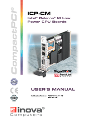
Inova PD00941013.001 User Manual (103 pages)
Intel Celeron M Low Power CPU Boards
Brand:
Inova
| Category:
Motherboard
| Size: 2.91 MB
Table of Contents
Preface
3
Table of Contents
3
Unpacking and Special Handling Instructions
8
Revision History
9
Three Year Limited Warranty
10
Product Overview Product Overview 1
11
Icp-CM Cpu
13
Product Overview
13
Interfacing
14
Peripherals
14
Software
14
Graphics
14
Specifications
15
Functional Overview
17
Figure 1.20 ICP-CM Interfacing
17
Figure 1.21 ICP-CM Board Overview
18
Software
19
Windows XP (Professional / Embedded)
19
Windows 2000 (Professional)
19
Linux
19
Venturecom
19
Windows CE
20
Vxworks
20
X86
20
Qnx
20
Jbed
20
Os-9 X
20
Hardware
21
Block Diagram
21
Figure 1.41 Block Diagram
21
Connector Location
22
Figure 1.42 Connector Locations
22
Connector Description
22
Table 1.43 Connector Description
22
Table 1.43 Continued
23
Front-Panel Features
23
Table 1.44 Front Panels
23
Figure 1.44 Front-Panel Options
24
Interface Positions
25
Figure 1.45 Interfaces
25
Construction - 4HP Standard CPU
26
Figure 1.46 Construction of CPU with Heat-Sink Assembly
26
Construction - 8HP Standard CPU
27
Figure 1.47 Construction of CPU with Heat-Sink Assembly
27
Construction - 8HP Standard CPU with AGP
28
Figure 1.48 Construction of CPU with Heat-Sink Assembly
28
Power Requirements
29
Table 1.49 ICP-CM Power Reqirements
29
Power Consumption
30
Figure 1.50 ICP-CM Power Consumption
30
Thermal Considerations
31
Table 1.51 ICP-CM Airflow Requirements
31
2 Configuration Con- Tents
33
Memory Map
34
Figure 2.00 System Architecture
34
Doc. PD00941013.001 ©2004 Inova Computers Gmbh Page
35
I/O Mapped Peripherals
36
Table 2.10 Legacy I/O Map (ISA Compatible)
36
Table 2.10 Legacy I/O Map (ISA Compatible) Contd
37
Memory Mapped Peripherals
38
Interrupt Routing
38
Table 2.30 PC-AT Interrupt Definitions
39
DMA Channel Descriptions
39
Table 2.40 DMA Channel Description
39
Inova CM SMB Devices
40
Table 2.50 SMB Devices
40
Inova CM PCI Device List
41
Table 2.60 Legacy I/O Map (ISA Compatible)
41
Interrupt Configuration
42
Table 2.70 Compactpci Bus Interrupts
42
Timer / Counter
43
Watchdog
43
Interfaces
45
Compactpci J1/J2 Connectors
46
Compactpci Connector Naming
46
Figure 3.01 Naming Convention as Per PICMG 2.0 R3.0 Specification
46
Compactpci J1 Connector
46
Figure 3.02 J1- 32-Bit Compactpci Bus Interface Connector
46
Table 3.03 32-Bit Compactpci J1 Pin Assignment
47
Table 3.04 32-Bit Compactpci J2 Pin Assignment (Std. with Rear I/O (D))
48
Table 3.04 32-Bit Compactpci J2 Pin Assignment (Std. - with Rear I/O (D)) - Contd
49
Table 3.05 Inova's ICP-CM Rear I/O J2 (CPU) Integration
50
Interfaces
51
Compactpci Backplane
51
Interfaces
52
Figure 3.10 Inova's 32-Bit Compactpci 8-Slot Backplane - RH System Slot
52
Figure 3.21 RJ45 Pinout
53
J6 & J7 Ethernet
53
Table 3.21 Ethernet Standards & Connector Signals
53
Graphic Features (Chipset)
54
J17 VGA Interface
54
Table 3.23A Highlights Just some of the Features of the Standard Integrated Video Controller
54
Figure 3.23 High-Density D-Sub VGA Interface Pinout
55
Table 3.23B Video Output Connector Signals
55
Figure 3.24 USB Interface Pinout
56
J19 USB Interface
56
Table 3.24 USB Connector Signals
56
Connecting the CM to a Slim-Line Floppy-Disk
57
Connecting the CM to the Inova ICP-HD3(-ND)
57
Connecting the CM to the Inova IPB-FPE12
57
J10 Hot-Swap Interface
57
J9 Compactflash Interface
57
SW1 Reset Button
57
Icp-Hd-3
59
A1 ICP-HD-3(-ND) CPU Extension
60
A1.1 ICP-HD-3(-ND) Front-Panels (8HP or 12HP
60
Figure A1.1 ICP-HD-3(-ND) CPU Front-Panels
60
A1.2 IDE Carrier Board ICP-HD-3(-ND
61
Figure A1.2 Interface Location of the ICP-HD-3(-ND) Module
61
Table A1.2 Interface Description of the ICP-HD-3(-ND) Module
62
A2 ICP-HD-3(-ND) Interfaces
63
A2.1 COM1 & COM2 Interfaces
63
Figure A2.1 COM1 & COM2 Interface Pinout
63
Table A2.1 COM1 & COM2 Connector Signals
63
A2.2 Mouse & Keyboard Interfaces
64
Figure A2.2 Mouse & Keyboard Interface Pinout
64
Table A2.2 Mouse & Keyboard Connector Signals
64
Table A2.3 USB Connector Signals
65
A2.3 USB 2.0 Interfaces
65
Figure A2.3 USB Interface Pinout
65
A2.4 EIDE Interface
66
A2.5 Slim-Line Floppy Disk Interface
66
Ipb-Fpe12
67
B1 IPB-FPE12 CPU Extension
68
B1.1 J13 Interface for LPT1
68
B1.2 IPB-FPE12 Front-Panel (4HP or 12HP
68
Figure B1.2 IPB-FPE12 Stand-Alone or Integrated with CPU
68
B1.3 LPT1 Piggyback
69
Table B1.3 IPB-FPE12 Connector Description
70
B1.4 LPT1 Interface
70
Table B1.4 LPT1 Connector Signals
70
Itm-Rio
71
C1 ITM-RIO CPU Extension
72
C1.1 ITM-RIO-D Configurations
72
Table C1.10 Valid Rear I/O Configurations
72
Table C1.11 Rear I/O Module Functionality
72
C1.2 ITM-RIO Rear-Panels (4HP or 8HP
73
Figure C1.2 the Rear Panels of the Inova ITM-RIO-D-X
73
C1.3 ITM-RIO-D-X Transition Module
74
Figure C1.3 Inova Rear I/O Transition Module ITM-RIO-D-X
74
Table C1.3 ITM-RIO-D-X Connector Description
75
C1.4 COM1 & COM2 Interfaces
76
Figure C1.4 COM1 & COM2 Interface Pinout
76
Table C1.4 COM1 & COM2 Connector Signals
76
C1.5 LPT1 Interface
77
Table C1.5 LPT1 Connector Signals
77
C1.6 Mouse & Keyboard Interfaces
78
Figure C1.6 Mouse & Keyboard Interface Pinout
78
Table C1.6 Mouse & Keyboard Connector Signals
78
C1.7 VGA Interface
79
Table C1.7 Video Output Connector Signals
79
C1.8 Fast Ethernet Interface
80
Table C1.8 Fast Ethernet Connector Signals
80
C1.9 USB Interface (USB 4
81
Table C1.9 USB Connector Signals
81
C1.10 EIDE Interface
82
C1.11 Slim-Line Floppy Disk Interface
82
C1.12 ITM-RIO(C&D)-FHLU Extension
83
Figure C1.12 ITM-RIO(C&D)-FHLU
83
Ipm-Ata
85
D1 IPM-ATA CPU Extension
86
D1.1 Rj2 Interface
86
Figure D1.1A Dedicated IPM-ATA Backplane
86
D1.1 Rj2 Interfaces (Contd
87
Figure D1.1B the Complete Connection Picture
87
D1.2 Ipm-Ata-Hd
88
D1.3 Ipm-Ata-Cf
89
D1.4 Ipm-Ata-Pcmcia
90
D1.5 Device Compatibility
91
Table D1.5 Compatibility List
91
E1 AGP-R7000 CPU Extension
94
Table E1.00 AGP Piggyback Configurations
94
E1.1 Specifications
95
E1.2 J4 Interface
96
Figure E1.20 J4 on the Underside of the AGP-R7000 Piggyback
96
Table E1.20 J4 Pinout
97
Table E1.20 J4 Pinout - Contd
98
E1.3 J3 & J5 IBP-GS-MULTILINK (TFT) Interfaces
99
Figure E1.30 J3 and J5 Topside Connectors for the Inova IPB-GS-MULTILINK
99
Table E1.30 J3 & J5 Interface Pinout
100
E1.4 J1 Front-Panel VGA/TMDS Interface
101
Figure E1.40 Standard Front-Panel VGA/TMDS Interface
101
Table E1.40 J1 Standard Front-Panel VGA/TMDS Pinout
101
Table E1.41 J2 DIP Switch Settings - Digital TMDS (Panellink) or DVI-D
102
Table E1.42 J2 DIP Switch Settings - TFT (24Bit TTL/CMOS)
102
E1.5 Rear I/O VGA Interface
103
Advertisement
Advertisement
Related Products
Inova ICP-CM
Inova Categories
Indoor Furnishing
Fitness Equipment
Tablet
Computer Hardware
Vacuum Cleaner
More Inova Manuals
Login
Sign In
OR
Sign in with Facebook
Sign in with Google
Upload manual
Upload from disk
Upload from URL