Sony DVP-S530D Service Manual
Cd/dvd player
Hide thumbs
Also See for DVP-S530D:
- Operating instructions manual (132 pages) ,
- Training manual (92 pages) ,
- Operating instructions manual (66 pages)
Table of Contents
Advertisement
DVP-S330/S530D/S550D/S705D
SERVICE MANUAL
CD/DVD player
Laser
Semiconductor laser
Signal format system
NTSC
Audio characteristics
Frequency response
DVD (PCM 96 kHz): 2 Hz to 44 kHz
(±1 dB)*
DVD (PCM 48 kHz): 2 Hz to 22 kHz
(±0.5 dB)
CD: 2 Hz to 20 kHz (±0.5 dB)
Signal-to-noise ratio
More than 110 dB (LINE OUT (AUDIO 1,
2) connectors only)
Harmonic distortion
Less than 0.0025%
Dynamic range
More than 100 dB (DVD)
More than 97 dB (CD)
Wow and flutter
Less than detected value
(±0.001% W PEAK)
Outputs and inputs
Jack
type
LINE OUT
Phono
(AUDIO 1, 2)
jacks
DIGITAL OUT
Optical
(OPTICAL)
output
connector
DIGITAL OUT
Phono
(COAXIAL)
jack
LINE OUT
Phono
(VIDEO 1, 2)
jacks
S VIDEO OUT
4-pin
(1, 2)
mini DIN
COMPONENT
phono
VIDEO OUT
jacks
(Y, P
/B-Y,
B
P
/R-Y)
R
(EXCEPT S330)
PHONES
Phone
(EXCEPT S330)
jack
5.1CH
Phono
OUTPUT
jacks
(EXCEPT S330)
MICROFILM
SPECIFICATIONS
Output
Load impedance
level
2 Vrms
Over 10 kilohms
(at 50 kilohms)
–18 dBm
Wave length: 660 nm
0.5 Vp-p
75 ohms terminated
1.0 Vp-p
75 ohms,
sync negative
Y: 1.0 Vp-p
75 ohms,
sync negative
C: 0.286 Vp-p
75 ohms terminated
Y: 1.0 Vp-p
75 ohms,
sync negative
P
/B-Y,
B
P
/R-Y:
R
0.7 Vp-p
75 ohms
12 mW
32 ohms
2 Vrms
Over 10 kilohms
(at 50 kilohms)
RMT-D108A/D109A/D111A/D111E
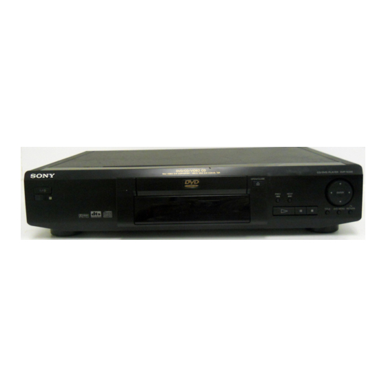
Photo: DVP-S330
General
Power requirements
Power consumption
Dimensions (approx.)
Mass (approx.)
Operating temperature
Operating humidity
Supplied accessories
• Audio/Video/S-link connecting cord (1) (US, Canadian)
• Audio/Video connecting cord (1) (E, Hong Kong, Singapore)
• S video cable (1)
• Remote commander (remote) RMT-D108A (1) (S530D)
• Remote commander (remote) RMT-D109A (1) (S330)
• Remote commander (remote) RMT-D111A (1) (S550D)
• Remote commander (remote) RMT-D111E (1) (S705D)
• Size AA (R6) batteries (2)
* The signals from LINE OUT (AUDIO 1, 2) connectors and 5.1 ch L, R
connectors (except S330) are measured. When you play the PCM sound
tracks with 96 kHz sampling frequency, the output signals from the
DIGITAL OUT (OPTICAL, COAXIAL) are converted to 48 kHz
(sampling frequency).
Design and specifications are subject to change without notice.
US Model
DVP-S330/S530D/S550D
Canadian Model
DVP-S330/S530D/S550D
E Model
DVP-S530D
Hong Kong Model
DVP-S705D
Singapore Model
DVP-S705D
120 V AC, 60 Hz
14 W (S330)
16 W (EXCEPT S330)
430 × 95 × 305 mm
(17 × 3
× 12 in.) (w/h/d)
3
/
4
incl. projecting parts
3.3 kg (7 lb 4 oz) (S330)
3.4 kg (7 lb 8 oz) (EXCEPT S330)
41°F to 95°F (5°C to 35°C)
5% to 90%
CD/DVD PLAYER
Advertisement
Table of Contents

Related Manuals for Sony DVP-S530D


Summary of Contents for Sony DVP-S530D
- Page 1 DVP-S330/S530D/S550D/S705D RMT-D108A/D109A/D111A/D111E SERVICE MANUAL US Model DVP-S330/S530D/S550D Canadian Model DVP-S330/S530D/S550D E Model DVP-S530D Hong Kong Model DVP-S705D Singapore Model DVP-S705D Photo: DVP-S330 SPECIFICATIONS CD/DVD player General Laser Power requirements Semiconductor laser 120 V AC, 60 Hz Signal format system NTSC...
- Page 2 SONY PARTS WHOSE PART NUMBERS APPEAR AS DE FONCTIONNEMENT. NE REMPLACER CES COM- SHOWN IN THIS MANUAL OR IN SUPPLEMENTS PUB- POSANTS QUE PAR DES PIÈCES SONY DONT LES LISHED BY SONY. NUMÉROS SONT DONNÉS DANS CE MANUEL OU DANS LES SUPPLÉMENTS PUBLIÉS PAR SONY.
-
Page 3: Table Of Contents
TABLE OF CONTENTS Section Title Page Section Title Page Service Note ................4 AU-212 (AUDIO, VIDEO BUFFER) Printed Wiring Board ............. 4-53 GENERAL AU-212 (AUDIO) Schematic Diagram ......4-55 AU-212 (VIDEO BUFFER) Schematic Diagram ... 4-57 FL-97/101 (FUNCTION SWITCH, IF CON) This Player Can Play the Following Discs .... -
Page 4: Service Note
SERVICE NOTE 1. DISASSEMBLY • This set can be disassembled in the order shown below. Case (Page 2-1) AU-208 Board AU-210 Board AU-212 Board Power MB-82/85 Tray Cover (S330) (S705D) (S530D/S550D) Block Board (Page 2-2) (Page 2-1) (Page 2-1) (Page 2-1) (Page 2-2) (Page 2-1) Mechanism... - Page 5 2. NOTE ON REMOVE THE CASE 4. HOW TO SERVICE MB-82/85 BOARD 1) Remove seven screws. (See Fig. 1) 1) Remove the case from the set. (Refer to 2-1) 2) Open the side of case. (See Fig. 1) 2) Remove the MB-82/85 board. (Refer to 2-2) 3) Remove the case as lift straight.
-
Page 6: General
DVP-S330/S530D/S550D/S705D SECTION 1 This section is extracted from DVP-S550D GENERAL instruction manual (3-865-641-11). - Page 15 1-10...
- Page 16 1-11...
- Page 17 1-12...
- Page 18 1-13...
- Page 19 1-14...
- Page 20 1-15...
- Page 21 1-16 E 1-16...
-
Page 22: Disassembly
DVP-S330/S530D/S550D/S705D SECTION 2 DISASSEMBLY Note: Follow the disassembly procedure in the numerical order given. 2-1. CASE REMOVAL 2-3. AU-208/212 BOARD REMOVAL (S330/S530D/S550D) 4 Case 3 Two flat cables 7 Three screws (CN302, 303) (B3) (S530D/S550D) 2 Two screws 2 Connector 4 Flat cable (CN401) (S530D/S550D) -
Page 23: Power Block Removal
2-5. POWER BLOCK REMOVAL 2-7. FRONT PANEL REMOVAL 2 Connector 4 Screw 3 Three connectors (CN101) (B3) (CN201, 202, 203) (S530D/S550D/S705D) 1 Connector 2 Connector 6 Boss (CN102) (CN701) (S705D) (S530D/S550D/S705D) 4 Four screws 1 Connector 5 Two screws (B3) 7 Boss (CN203) (B3) -
Page 24: Tray Removal
2-9. TRAY REMOVAL 2-11. BELT, LOADING MOTOR (M001), MS-29/TK-51 BOARD REMOVAL 1 Two screws (BTP2.6 × 12) 1 Belt 2 Chuck ass’y 2 Two screws (B2.6 × 4) 9 TK-51 board 6 Flexible board (CN001) 8 Claw 4 Remove the tray in the direction of the arrow B. -
Page 25: Internal View
2-12. INTERNAL VIEW DC motor (loading) Optical pick-up (KHM-220AAA/J1RP) 1-541-632-11 8-820-081-03... -
Page 26: Circuit Boards Location
2-13. CIRCUIT BOARDS LOCATION Power Block SRV902UC (S330/S530: US, Canadian/S550D) HS-030SH (S705D) HS-030SF (S530D: E) (SWITCHING REGULATOR) TK-51 (RF/SERVO) RY-12 (S705D) (RELAY) FR-146 (S330) AU-208 (S330) FR-148 (S705D) AU-210 (S705D) FR-150 (S530D/S550D) AU-212 (S530D/S550D) (IR/POWER SWITCH) (AUDIO) HP-109 (S705D) HP-111 (S530D/S550D) (HEADPHONE) MS-29 (LOADING) -
Page 27: Block Diagrams
DVP-S330/S530D/S550D/S705D SECTION 3 BLOCK DIAGRAMS 3-1. OVERALL BLOCK DIAGRAM MB-82/85 BOARD S550D/S705D (SEE PAGE 4-21~37) IC502 IC304 IC402, 403 V EQ/NR 16M DRAM 16M SDRAM BASE UNIT TK-51 BOARD AU-208/210/212 BOARD KHM-220AAA (SEE PAGE 4-13) (SEE PAGE 4-43,49,51,55,57) VIDEO V, OPTICAL DEVICE VIDEO Y, VIDEO 1, 2... -
Page 28: Rf/Servo Block Diagram
DVP-S330/S530D/S550D/S705D 3-2. RF/SERVO BLOCK DIAGRAM IC001%¢(DVD play) BASE UNIT TK-51 BOARD MB-82/85 BOARD(1/6) (SEE PAGE 4-25,27) (SEE PAGE 4-13) 500mV/DIV 100ns/DIV KHM-220AAA IC0011(DVD play) IC001$º(CD play) IC001$º(DVD play) 200mV/DIV 100ns/DIV IC701^•(DVD play) 100mV/DIV 50ms/DIV 500mV/DIV 50ms/DIV IC701^ª(DVD play) 100mV/DIV 5ms/DIV 500mV/DIV 50ms/DIV 1.5Vp-p IC001%¢(CD play) -
Page 29: Signal Process/Video Block Diagram
DVP-S330/S530D/S550D/S705D 3-3. SIGNAL PROCESS/VIDEO BLOCK DIAGRAM S550D/S705D MB-82/85 BOARD(2/6) (SEE PAGE 4-21,23,29,35,37) IC502 IC303!¶(DVD play) V EQ/NR 500mV/DIV 100ns/DIV IC304 IC402, 403 16M DRAM 16M SDRAM IC401%¢ AU-208/212 BOARD(1/3) 1.6Vp-p 11-18 60-67 97 98 31 29 AU-210 BOARD(1/2) IC401%• IC303!ª(CD play) (SEE PAGE 4-43,49,51,55,57) 500mV/DIV 200ns/DIV 720mVp-p(H) -
Page 30: System Control Block Diagram
DVP-S330/S530D/S550D/S705D 3-4. SYSTEM CONTROL BLOCK DIAGRAM MB-82/85 BOARD(3/6) (SEE PAGE 4-31,33,35) IC204 IC205 1M SRAM 16M FLASH S550D/S705D HA 0-21 SIGNAL PROCESS, VIDEO IC602 +3.3V IC207 AUDIO 1 (SEE PAGE 3-5) HD 0-15 IC201 16M NAND-F (SEE PAGE 3-9) POWER ON 146-154 126-133 4K EEPROM... -
Page 31: Audio (1) Block Diagram
DVP-S330/S530D/S550D/S705D 3-5. AUDIO (1) BLOCK DIAGRAM MB-82/85 BOARD(4/6) (SEE PAGE 4-35,37) S330 R502 SPDIF1 SPDIF R536 R538 LRCK R529 ACH12 S530D/S550D/S705D IC902 AUDIO 2CH DAC SIGNAL PROCESS, BCLKIN V OUT L BCKI BCKO AUDIOLT VIDEO IC501 (SEE PAGE 3-6) LRCKO LRCIN V OUT R AUDIORT... -
Page 32: Audio (2) Block Diagram
DVP-S330/S530D/S550D/S705D 3-6. AUDIO (2) BLOCK DIAGRAM – DVP-S330/S530D/S550D – AU-208/212 BOARD(2/3) J502 MB-82/85 BOARD(5/6) (SEE PAGE 4-43,55,57) (SEE PAGE 4-37) Q341 COAXIAL BUFFER INTERFACE DIGITAL IC505 A MUTE CONTROL S330 D IN (SEE PAGE 3-16) OPTICAL MA MUTE J505 SYSTEM CONTROL GAIN1 (SEE PAGE 3-7,8) GAIN2... -
Page 33: Audio (3) Block Diagram
DVP-S330/S530D/S550D/S705D 3-7. AUDIO (3) BLOCK DIAGRAM – DVP-S705D – AU-210 BOARD(2/2) J301 MB-82/85 BOARD(5/6) (SEE PAGE 4-49,51) (SEE PAGE 4-37) Q303 COAXIAL BUFFER INTERFACE DIGITAL IC303 A MUTE CONTROL (SEE PAGE 3-16) D IN OPTICAL MA MUTE J304 SYSTEM CONTROL (SEE PAGE 3-7,8) GAIN2 AUDIO OUT1... -
Page 34: Interface Control Block Diagram
DVP-S330/S530D/S550D/S705D 3-8. INTERFACE CONTROL BLOCK DIAGRAM S330/S530D: US, Canadian/S550D MB-82/85 BOARD(6/6) AU-208/212 BOARD(3/3) (SEE PAGE 4-31,37) (SEE PAGE 4-55,57) CN301 CN005 SLINK J501 S-LINK FL-97/99/101 BOARD (SEE PAGE 4-65,67) FR-146/148/ SLINK 150 BOARD (SEE PAGE 4-71) IC203 S-LINK SCLK1 IFSC0 CONTROL STATUS IN STATUS<N>... -
Page 35: Power Block Diagram
DVP-S330/S530D/S550D/S705D 3-9. POWER BLOCK DIAGRAM S705D S330/S530D: US, Canadian/S550D/S705D CN201 CN101 D401-404 CN102 CN401 HS-030SF/030SH BOARD RY101 T901 IC412, (SEE PAGE 4-79) ACOUT L, N ACOUT L, N AC10V IC415 RCORE IC303 Q420, 421 +5V REG TRANS +9V, –9V CN407 CN202 CN201 CN101... -
Page 36: Printed Wiring Boards And Schematic Diagrams
DVP-S330/S530D/S550D/S705D SECTION 4 PRINTED WIRING BOARDS AND SCHEMATIC DIAGRAMS THIS NOTE IS COMMON FOR PRINTED WIRING For schematic Diagram: • Caution when replacing chip parts. BOARDS AND SCHEMATIC DIAGRAMS. New parts must be attached after removal of chip. (In addition to this, the necessary mote is printed Be careful not to heat the minus side of tantalum capacitor, in each block.) because it is damaged by the heat. -
Page 37: Frame Schematic Diagram
DVP-S330/S530D/S550D/S705D 4-1. FRAME SCHEMATIC DIAGRAM FRAME (1) SCHEMATIC DIAGRAM FRAME (1/3) - Page 38 DVP-S330/S530D/S550D/S705D FRAME (2) SCHEMATIC DIAGRAM – DVP-S330/S530D/S550D – FRAME (2/3)
- Page 39 DVP-S330/S530D/S550D/S705D FRAME (3) SCHEMATIC DIAGRAM – DVP-S705D – FRAME (3/3)
-
Page 40: Printed Wiring Boards And Schematic Diagrams
DVP-S330/S530D/S550D/S705D There are few cases that the part isn't mounted in this model is printed on this diagram. 4-2. PRINTED WIRING BOARDS AND SCHEMATIC DIAGRAMS TK-51 TK-51 (RF/SERVO) PRINTED WIRING BOARD BOARD(SIDE A) – Ref. No.: TK-51 board; 2,000 series – TK-51 BOARD (SIDE A) CN001 CN002... - Page 41 DVP-S330/S530D/S550D/S705D • Waveforms 1 IC001 1 (DVD play) 6 IC001 #ª (CD play) TK-51 200 mV/DIV 100 ns/DIV 500 mV/DIV 200 ms/DIV BOARD(SIDE B) 536 mVp-p 1.7 Vp-p 2 IC001 1 (CD play) 7 IC001 $º (DVD play) 500 mV/DIV 500 ns/DIV 100 mV/DIV 50 ms/DIV 880 mVp-p 180 mVp-p...
-
Page 42: Rf/Servo) Schematic Diagram
DVP-S330/S530D/S550D/S705D TK-51 (RF/SERVO) SCHEMATIC DIAGRAM • See page 4-9 for printed wiring board and page 4-12 for waveforms. – Ref. No.: TK-51 board; 2,000 series – Note: Note: The components identi- Les composants identifiés par fied by mark ! or dotted une marque ! sont critiques line with mark ! are criti- pour la sécurité. -
Page 43: Loading) Printed Wiring Board And Schematic Diagram
DVP-S330/S530D/S550D/S705D MS-29 (LOADING) PRINTED WIRING BOARD AND SCHEMATIC DIAGRAM – Ref. No.: MS-29 board; 3,000 series – There are few cases that the part isn't mounted in this model is printed on this diagram. MS-29 BOARD S001 (TRAY SENSOR) S001 CN001 LOADING MOTOR... -
Page 44: Mb-82/85 (Signal Process) Printed Wiring Board
DVP-S330/S530D/S550D/S705D MB-82/85 (SIGNAL PROCESS) PRINTED WIRING BOARD There are few cases that the part isn't mounted in this model is printed on this diagram. – Ref. No.: MB-82/85 board; 1,000 series – MB-82/85 BOARD(SIDE A) MB-82/85 BOARD (SIDE A) CN001 CN002 CN003 CN004... - Page 45 DVP-S330/S530D/S550D/S705D MB-82/85 BOARD(SIDE B) MB-82/85 BOARD (SIDE B) D701 D806 IC005 IC201 IC203 IC204 IC207 IC304 IC402 IC403 IC404 IC502 IC602 IC702 IC801 IC802 IC803 IC902 IC905 IC906 IC907 (11) MB-82 : 1-672-676- MB-85 : 1-672-751- SIGNAL PROCESS MB-82/85 4-19 4-20...
-
Page 46: Mb-82/85 (Av Decoder) Schematic Diagram
DVP-S330/S530D/S550D/S705D MB-82/85 (AV DECODER) SCHEMATIC DIAGRAM • See page 4-17 for printed wiring board. – Ref. No.: MB-82/85 board; 1,000 series – AV DECODER MB-82/85 (1/10) 4-21 4-22... -
Page 47: Mb-82/85 (Sdram) Schematic Diagram
DVP-S330/S530D/S550D/S705D MB-82/85 (SDRAM) SCHEMATIC DIAGRAM • See page 4-17 for printed wiring board. – Ref. No.: MB-82/85 board; 1,000 series – • Waveforms 1 IC401 %¢ 5 IC401 ^™ 816 mVp-p (H) 720 mVp-p (H) 2 IC401 %¶ 6 IC401 ^∞ 1.2 Vp-p (H) 728 mVp-p (H) 3 IC401 %•... -
Page 48: Mb-82/85 (Servo Dsp) Schematic Diagram
DVP-S330/S530D/S550D/S705D MB-82/85 (SERVO DSP) SCHEMATIC DIAGRAM • See page 4-17 for printed wiring board. • Waveforms – Ref. No.: MB-82/85 board; 1,000 series – 1 IC701 ^ª (DVD play) 500 mV/DIV 50 ms/DIV 1.4 Vp-p 2 IC701 ^ª (CD play) 500 mV/DIV 200 mV/DIV 1.7 Vp-p 3 IC701 ^•... -
Page 49: Mb-82/85 (Drive) Schematic Diagram
DVP-S330/S530D/S550D/S705D MB-82/85 (DRIVE) SCHEMATIC DIAGRAM • See page 4-17 for printed wiring board. – Ref. No.: MB-82/85 board; 1,000 series – DRIVE MB-82/85 (4/10) 4-27 4-28... -
Page 50: Mb-82/85 (Arp) Schematic Diagram
DVP-S330/S530D/S550D/S705D MB-82/85 (ARP) SCHEMATIC DIAGRAM • See page 4-17 for printed wiring board. – Ref. No.: MB-82/85 board; 1,000 series – • Waveforms 1 IC303 !¶ (DVD play) 500 mV/DIV 100 ns/DIV 1.6 Vp-p 2 IC303 !ª (CD play) 500 mV/DIV 200 ns/DIV 1.6 Vp-p MB-82/85 (5/10) 4-29... -
Page 51: Mb-82/85 (System Control) Schematic Diagram
DVP-S330/S530D/S550D/S705D MB-82/85 (SYSTEM CONTROL) SCHEMATIC DIAGRAM • See page 4-17 for printed wiring board. – Ref. No.: MB-82/85 board; 1,000 series – • Waveforms 1 IC202 (™ 2.4 Vp-p (12.5 MHz) 2 IC202 5 4 Vp-p (25.3 MHz) SYSTEM CONTROL MB-82/85 (6/10) 4-31 4-32... -
Page 52: Mb-82/85 (Hga) Schematic Diagram
DVP-S330/S530D/S550D/S705D MB-82/85 (HGA) SCHEMATIC DIAGRAM • See page 4-17 for printed wiring board. – Ref. No.: MB-82/85 board; 1,000 series – MB-82/85 (7/10) 4-33 4-34... -
Page 53: Mb-82/85 (Clock Generator, Audio Dsp, V Eq/Nr) Schematic Diagram
DVP-S330/S530D/S550D/S705D MB-82/85 (CLOCK GENERATOR, AUDIO DSP, V EQ/NR) SCHEMATIC DIAGRAM • See page 4-17 for printed wiring board and page 4-40 for waveforms. – Ref. No.: MB-82/85 board; 1,000 series – CSYNCO COUNT1 COUNT2 COUNT3 IF SEL0 IF SEL1 FNR_ON FNR_LVL0 FNR_LVL1 FNR_UFRZ... -
Page 54: Mb-82/85 (Dac) Schematic Diagram
DVP-S330/S530D/S550D/S705D MB-82/85 (DAC) SCHEMATIC DIAGRAM • See page 4-17 for printed wiring board. – Ref. No.: MB-82/85 board; 1,000 series – MB-82/85 (9/10) 4-37 4-38... -
Page 55: Mb-82/85 (Bias) Schematic Diagram
DVP-S330/S530D/S550D/S705D MB-82/85 (BIAS) SCHEMATIC DIAGRAM • See page 4-17 for printed wiring board. • Waveforms – Ref. No.: MB-82/85 board; 1,000 series – 1 IC004 2, 5, 7 6 IC001 !¢ (DVD play) 4.2 Vp-p (25.3 MHz) 4.2 Vp-p (26.9 MHz) 2 IC003 5, 7 7 IC001 !¢... -
Page 56: Audio, Video Buffer) Printed Wiring Board
DVP-S330/S530D/S550D/S705D AU-208 (AUDIO, VIDEO BUFFER) PRINTED WIRING BOARD There are few cases that the part isn't mounted in this model is printed on this diagram. – Ref. No.: AU-208 board; 2,000 series – – DVP-S330 – AU-208 BOARD AU-208 BOARD CN301 DIGITAL OUT LINE OUT... -
Page 57: Audio, Video Buffer) Schematic Diagram
DVP-S330/S530D/S550D/S705D AU-208 (AUDIO, VIDEO BUFFER) SCHEMATIC DIAGRAM – Ref. No.: AU-208 board; 2,000 series – – DVP-S330 – AUDIO, VIDEO BUFFER AU-208 4-43 4-44... -
Page 58: Audio, Video Buffer) Printed Wiring Board
DVP-S330/S530D/S550D/S705D AU-210 (AUDIO, VIDEO BUFFER) PRINTED WIRING BOARD – Ref. No.: AU-210 board; 3,000 series – There are few cases that the part isn't mounted in this model is printed on this diagram. – DVP-S705D – AU-210 BOARD(SIDE A) 1-672-248- (11) Power Block SRV902UC (S330/S530: US, Canadian/S550D) - Page 59 DVP-S330/S530D/S550D/S705D AU-210 BOARD (SIDE B) AU-210 BOARD(SIDE B) CN301 COMPONENT VIDEO OUT CN401 C-11 AUDIO OUT 5.1CH OUTPUT DIGITAL OUT VIDEO CN402 OPTICAL COAXIAL /B-Y /R-Y FRONT REAR CENTER/WOOFER CN403 CN404 CN405 S VIDEO CN407 D301 D302 D303 D304 D401 C-11 D402 C-11...
-
Page 60: Au-210 (Audio) Schematic Diagram
DVP-S330/S530D/S550D/S705D AU-210 (AUDIO) SCHEMATIC DIAGRAM • See page 4-45 for printed wiring board. – Ref. No.: AU-210 board; 3,000 series – – DVP-S705D – AUDIO AU-210 (1/2) 4-49 4-50... - Page 61 DVP-S330/S530D/S550D/S705D AU-210 (VIDEO BUFFER) SCHEMATIC DIAGRAM • See page 4-45 for printed wiring board. – Ref. No.: AU-210 board; 3,000 series – – DVP-S705D – • Waveforms 1 IC301 2 6 IC301 !∞ 2.0 Vp-p (H) 1.1 Vp-p (H) 2 IC301 4 1.2 Vp-p (H) 3 IC301 7 860 mVp-p (H)
- Page 62 DVP-S330/S530D/S550D/S705D AU-212 (AUDIO, VIDEO BUFFER) PRINTED WIRING BOARD There are few cases that the part isn't mounted in this model is printed on this diagram. – Ref. No.: AU-212 board; 2,000 series – – DVP-S530D/S550D – AU-212 BOARD DIGITAL OUT...
- Page 63 DVP-S330/S530D/S550D/S705D AU-212 (AUDIO) SCHEMATIC DIAGRAM – Ref. No.: AU-212 board; 2,000 series – – DVP-S530D/S550D – AUDIO AU-212 (1/2) 4-55 4-56...
-
Page 64: Printed Wiring Board
AU-212 (VIDEO BUFFER) SCHEMATIC DIAGRAM • See page 4-53 for printed wiring board. • Waveforms – Ref. No.: AU-212 board; 2,000 series – 1 IC321 2 6 IC321 !∞ – DVP-S530D/S550D – 2.0 Vp-p (H) 1.1 Vp-p (H) 2 IC321 4 1.2 Vp-p (H) -
Page 65: Fl-97/101 (Function Switch, If Con) Printed Wiring Board
DVP-S330/S530D/S550D/S705D FL-97/101 (FUNCTION SWITCH, IF CON) PRINTED WIRING BOARD There are few cases that the part isn't mounted in this model is printed on this diagram. – Ref. No.: FL-97/101 board; 2,000 series – – DVP-S330/S530D/S550 – FL-97/101 BOARD FL-97/101 BOARD CN201 CN202... -
Page 66: Function Switch, If Con) Printed Wiring Board
DVP-S330/S530D/S550D/S705D FL-99 (FUNCTION SWITCH, IF CON) PRINTED WIRING BOARD There are few cases that the part isn't mounted in this model is printed on this diagram. – Ref. No.: FL-99 board; 2,000 series – – DVP-S705D – FL-99 BOARD(SIDE A) 1-672-249- (11) Power Block... - Page 67 DVP-S330/S530D/S550D/S705D FL-99 BOARD FL-99 BOARD(SIDE B) (SIDE B) CN201 CN202 C-10 PROGRAM CLEAR CN203 C-12 RETURN TITLE DVD MENU FLUORESCENT INDICATOR TUBE D202 A-10 D203 D204 C-13 D205 B-12 SHUFFLE D206 D207 REPEAT SEARCH IC201 IC202 A-10 SEARCH IC203 B-12 Q201 D204,S208 OPEN/CLOSE...
- Page 68 DVP-S330/S530D/S550D/S705D FL-97/99/101 (FUNCTION SWITCH) SCHEMATIC DIAGRAM • See pages 4-59 and 4-61 for printed wiring board. – Ref. No.: FL-97/99/101 board; 2,000 series – –30V REG FL-97/99/101 BOARD (2/2) FUNCTION SWITCH FL-97/99/101 (1/2) 4-65 4-66...
-
Page 69: Fl-97/99/101 (Function Switch)
DVP-S330/S530D/S550D/S705D FL-97/99/101 (IF CON) SCHEMATIC DIAGRAM • See pages 4-59 and 4-61 for printed wiring board. – Ref. No.: FL-97/99/101 board; 2,000 series – FL-97/99/101 BOARD (1/2) • Waveform 1 IC201 !¢ 3.9 Vp-p (4 MHz) IF CON FL-97/99/101 (2/2) 4-67 4-68... -
Page 70: Sw-315/317 (Surround Switch), Fr-146/148/150 (Ir/Power Switch) Printed Wiring Boards
SW-315/317 (SURROUND SWITCH), FR-146/148/150 (IR/POWER SWITCH) PRINTED WIRING BOARDS – Ref. No.: SW-315/317 board and FR-146/148/150 board; 4,000 series – There are few cases that the part isn't mounted in this model is printed on this diagram. – DVP-S530D/S550D – – DVP-S705D – – DVP-S330/S530D/S550D –... -
Page 71: Sw-315/317 (Surround Switch), Fr-146/148/150 (Ir/Power Switch) Schematic Diagram
DVP-S330/S530D/S550D/S705D SW-315/317 (SURROUND SWITCH), FR-146/148/150 (IR/POWER SWITCH) SCHEMATIC DIAGRAM – Ref. No.: SW-315/317 board and FR-146/148/150 board; 4,000 series – 4-72 SURROUND SWITCH, IR/POWER SWITCH SW-315/317, FR-146/148/150 4-71... -
Page 72: Hp-109/111 (Headphone) Printed Wiring Boards And Schematic Diagram
HP-109/111 (HEADPHONE) PRINTED WIRING BOARDS AND SCHEMATIC DIAGRAM – Ref. No.: HP-109/111 board; 2,000 series – There are few cases that the part isn't mounted in this model is printed on this diagram. – DVP-S530D/S550D/S705D – – DVP-S530D/S550D – HP-111... -
Page 73: Relay) Printed Wiring Board And Schematic Diagram
DVP-S330/S530D/S550D/S705D RY-12 (RELAY) PRINTED WIRING BOARD AND SCHEMATIC DIAGRAM – Ref. No.: RY-12 board; 2,000 series – There are few cases that the part isn't mounted in this model is printed on this diagram. – DVP-S705D – – DVP-S705D – RY-12 BOARD 1-672-888-... -
Page 74: Hs-030Sf/030Sh (Switching Regulator) Printed Wiring Board
DVP-S330/S530D/S550D/S705D HS-030SF/030SH (SWITCHING REGULATOR) PRINTED WIRING BOARD – Ref. No.: HS-030SF/030SH board; 6,000 series – – DVP-S530D: E/S705D – There are few cases that the part isn't mounted in this model is printed on this diagram. HS-030SF/030SH BOARD CN101 CN102... -
Page 75: Hs-030Sf/030Sh (Switching Regulator) Schematic Diagram
DVP-S330/S530D/S550D/S705D HS-030SF/030SH (SWITCHING REGULATOR) SCHEMATIC DIAGRAM – Ref. No.: HS-030SF/030SH board; 6,000 series – – DVP-S530D: E/S705D – HS-030SF/030SH BOARD T101 L211 P211 D211 10uH CN201 8P 500mA 60V S2L20U +3.3V C112 0.047uF AU-210 BOARD CN404 630V Q103 C213 C211... -
Page 76: Srv902Uc (Switching Regulator) Printed Wiring Board
DVP-S330/S530D/S550D/S705D SRV902UC (SWITCHING REGULATOR) PRINTED WIRING BOARD – Ref. No.: SRV902UC board; 7,000 series – – DVP-S330/S530D: US, CND/S550D – There are few cases that the part isn't mounted in this model is printed on this diagram. SRV902UC BOARD CN101 CN201 CN202 CN203... -
Page 77: Srv902Uc (Switching Regulator) Schematic Diagram
DVP-S330/S530D/S550D/S705D SRV902UC (SWITCHING REGULATOR) SCHEMATIC DIAGRAM – Ref. No.: SRV902UC board; 7,000 series – – DVP-S330/S530D: US, CND/S550D – SRV902UC BOARD T101 L201 D201 PS201 10uH FMX-12S 500mA D102 D101 C110 100p 1kV C104 C201 C202 R102 C102 IN4005 IN4005 D105 1000p 1000... -
Page 78: Ic Pin Function Description
DVP-S330/S530D/S550D/S705D SECTION 5 IC PIN FUNCTION DESCRIPTION 5-1 E... -
Page 79: Test Mode
DVP-S330/S530D/S550D/S705D SECTION 6 TEST MODE 6-1. GENERAL DESCRIPTION ### Syscon Diagnosis ### The Test Mode allows you to make diagnosis and adjustment eas- Diag All Check ily using the remote commander and monitor TV. The instructions, No. 2 Version diagnostic results, etc. are given on the on-screen display (OSD). 2-3. - Page 80 Model Type This test is skipped if “All” is selected. DVP-S330 (US, Canadian) Supplement: How to disconnect mechanical deck DVP-S530D (US, Canadian) Disconnect flat cables connected to the CN002 and CN003 DVP-S530D (E) of MB-82/85 board. Also, disconnect harness from the CN011.
- Page 81 The program code data stored in ROM are copied to all order. areas of RAM (IC304) connected to the ARP (IC303) For DVP-S530D/DVP-S550D/DVP-S705D through the bus, then they are read and checked if they ac- (DD models): cord. If the detail check was selected initially, the data are All channels →...
- Page 82 Check Items List Error Codes List 00: Error not detected 01: RAM write/read data discord 2) Version 02: Gate array NG (2-2) Revision 03: EEPROM NG (2-3) ROM Check Sum 04: Flash memory clear error (2-4) Model Type 05: Flash memory write error (2-5) Region 06: Flash memory read data discord 08: ARP register read data discord...
-
Page 83: Drive Auto Adjustment
6-4. DRIVE AUTO ADJUSTMENT 1. DVD-SL (single layer) [ENTER] Select , insert DVD single layer disc, and press key, On the Test Mode Menu screen, press key on the remote com- and the adjustment will be made through the following steps, then mander, and the drive auto adjustment menu will be displayed. - Page 84 2. CD 3. DVD-DL (dual layer) [ENTER] [ENTER] Select , insert CD disc, and press key, and the adjust- Select , insert DVD dual layer disc, and press key, ment will be made through the following steps, then adjusted val- and the adjustment will be made through the following steps, then ues will be written to the EEPROM.
-
Page 85: Drive Manual Operation
4. SACD 6-5. DRIVE MANUAL OPERATION [ENTER] Select , insert SACD disc, and press key, and the On the Test Mode Menu screen, select , and the manual opera- adjustment will be made through the following steps, then adjusted tion menu will be displayed. For the manual operation, each servo values will be written to the EEPROM. - Page 86 0. Disc Check Memory Disc Type 1. Disc Type Auto Check Disc Check 2. DVD SL 12 cm 3. DVD DL 12 cm 4. CD 12cm 5. SACD 12 cm 1. SL Disc Check 6. dvd SL 8 cm 7. DVD DL 8 cm 2.
-
Page 87: Mecha Aging
6-6. MECHA AGING Reset SLED TILT Reset the Sled and Tilt to initial posi- tion. ### Mecha Aging ### Turn ON/OFF the laser. Turn ON/OFF the spindle. Press OPEN key Focus Search the focus and turn on the focus. Turn ON/OFF the tracking servo. Sled Turn ON/OFF the sled servo. -
Page 88: Version Information
How to see Emergency History 6-8. VERSION INFORMATION ## Version Information ## IF con. Ver. x. xxx (xxxx) Group SYScon. Ver. x. xxx (xxxx) Model Region 1 : Emergency Code 2 : Don’t Care These codes are used for verification of software designing. 3 : Historical order 1 to 9 Exit: RETURN Emergency Codes List... -
Page 89: Electrical Adjustments
DVP-S330/S530D/S550D/S705D SECTION 7 ELECTRICAL ADJUSTMENTS 7-1. POWER SUPPLY ADJUSTMENT In making adjustment, refer to 7-3. Adjustment Related Parts Arrangement. 1. Power Supply Check (HS-030SF/030SH BOARD, SRV902UC BOARD) Note: During diagnostic check, the characters and color bars can be seen only with the NTSC monitor. Therefore, for diag- Mode nostic check, use the monitor that supports both NTSC and PAL modes... -
Page 90: Adjustment Of Video System
7-2. ADJUSTMENT OF VIDEO SYSTEM 3. Checking Component Video Output B-Y (MB-82/85 BOARD) (DVP-S530D/S550D/S705D) <Purpose> 1. Video Level Adjustment (MB-82/85 BOARD) This checks component video output B-Y. If it is incorrect, cor- <Purpose> rect colors will not be displayed when connected to, for instance, This adjustment is made to satisfy the NTSC standard, and if not projector. -
Page 91: Checking Component Video Output Y
5. Checking Component Video Output Y 7-3. ADJUSTMENT RELATED PARTS ARRANGEMENT (MB-82/85 BOARD) (DVP-S530D/S550D/S705D) <Purpose> MB-82/85 BOARD (SIDE A) This checks component video output Y. If it is incorrect, correct brightness will not be attained when connected to, for instance, projector. -
Page 92: Repair Parts List
DVP-S330/S530D/S550D/S705D SECTION 8 REPAIR PARTS LIST 8-1. EXPLODED VIEWS NOTE: The components identified by • The mechanical parts with no reference number in • -XX and -X mean standardized parts, so they may mark ! or dotted line with mark the exploded views are not supplied. -
Page 93: Case Assembly (S705D)
8-1-2. CASE ASSEMBLY (S705D) Front panel section Ref. No. Part No. Description Remark Ref. No. Part No. Description Remark 3-053-493-01 ORNAMENT (M), TRAY 3-053-984-01 SCREW (+BV/CU) 3-053-492-01 ORNAMENT (AL), TRAY (Hong Kong) X-3602-115-1 FOOT ASSY 3-053-492-21 ORNAMENT (AL), TRAY (Singapore) 1-418-321-61 COMMANDER, STANDARD (RMT-D111E/N) 3-975-726-31 EMBLEM, DVD (Singapore) (Hong Kong) -
Page 94: Front Panel Assembly
3-945-284-51 KNOB, VOLUME (S530D/S550D) 3-974-997-51 WINDOW, REMOTE CONTROL (S705D: Singapore) 3-945-284-81 KNOB, VOLUME (S705D: Singapore) S530D/S550D/S705D 4-942-568-31 EMBLEM (NO.5), SONY (S705D: Hong Kong) 3-945-284-71 KNOB, VOLUME (S705D: Hong Kong) 2-118-268-01 NUT (M9), HEXAGON (S530D/S550D/S705D) 4-942-568-61 EMBLEM (NO.5), SONY (S705D: Singapore) * 121... -
Page 95: Chassis Assembly
not supplied T901 8-1-4. CHASSIS ASSEMBLY 8-1-5. MECHANISM DECK ASSEMBLY Mechanism deck not supplied S705D S330 S705D supplied S705D supplied supplied S530D/S550D supplied S530D/S550D/ S705D M001 supplied S530D/S550D/ S705D supplied supplied The components identified by mark Les composants identifiés par une ! or dotted line with mark ! are criti- marque ! sont critiquens pour la cal for safety. -
Page 96: Electrical Parts List
AU-208 AU-212 8-2. ELECTRICAL PARTS LIST NOTE: The components identified by • Due to standardization, replacements in the • Items marked “*” are not stocked since they mark ! or dotted line with mark parts list may be different from the parts speci- are seldom required for routine service. - Page 97 AU-208 AU-212 Ref. No. Part No. Description Remark Ref. No. Part No. Description Remark C509 1-136-850-11 FILM 0.1uF D525 8-719-988-61 DIODE 1SS355TE-17 (S530D/S550D) (S530D/S550D) D526 8-719-988-61 DIODE 1SS355TE-17 (S530D/S550D) C512 1-136-850-11 FILM 0.1uF D551 8-719-988-61 DIODE 1SS355TE-17 (S530D/S550D) (S530D/S550D) D552 8-719-988-61 DIODE 1SS355TE-17 (S530D/S550D) C513 1-104-664-11 ELECT...
- Page 98 AU-208 AU-212 Ref. No. Part No. Description Remark Ref. No. Part No. Description Remark < JACK > < COIL > J303 1-784-675-21 JACK, PIN 3P (COMPONENT VIDEO OUT) L301 1-412-953-11 INDUCTOR 15uH (S530D/S550D) L302 1-412-953-11 INDUCTOR 15uH J501 1-764-188-21 JACK (SMALL TYPE) (DIA. 3.5) (S-LINK) L303 1-412-953-11 INDUCTOR 15uH...
- Page 99 AU-208 AU-212 Ref. No. Part No. Description Remark Ref. No. Part No. Description Remark R308 1-216-021-00 METAL CHIP 1/10W R410 1-216-025-91 RES,CHIP 1/10W (S530D/S550D) (S530D/S550D) R309 1-216-097-91 RES,CHIP 100K 1/10W R411 1-216-049-91 RES,CHIP 1/10W R310 1-216-042-00 METAL CHIP 1/10W (S530D/S550D) (S530D/S550D) R412 1-216-049-91 RES,CHIP...
- Page 100 AU-208 AU-212 AU-210 Ref. No. Part No. Description Remark Ref. No. Part No. Description Remark R511 1-216-069-00 METAL CHIP 6.8K 1/10W R562 1-216-049-91 RES,CHIP 1/10W (S530D/S550D) (S530D/S550D) R512 1-216-071-00 METAL CHIP 8.2K 1/10W R563 1-216-049-91 RES,CHIP 1/10W (S530D/S550D) (S330/S530D: US, Canadian/S550D) R564 1-216-295-91 SHORT 0 (S530D/S550D)
- Page 101 AU-210 Ref. No. Part No. Description Remark Ref. No. Part No. Description Remark C316 1-126-960-11 ELECT C452 1-136-850-11 FILM 0.1uF C317 1-163-259-91 CERAMIC CHIP 220PF C453 1-136-850-11 FILM 0.1uF C318 1-104-665-11 ELECT 100uF C454 1-119-828-31 ELECT 100uF C319 1-104-665-11 ELECT 100uF C455 1-124-673-11 ELECT...
- Page 102 AU-210 Ref. No. Part No. Description Remark Ref. No. Part No. Description Remark < EARTH TERMINAL > L403 1-412-953-11 INDUCTOR 15uH * ET401 1-537-738-21 TERMINAL, EARTH L404 1-412-953-11 INDUCTOR 15uH * ET402 1-537-738-21 TERMINAL, EARTH L405 1-412-953-11 INDUCTOR 15uH * ET403 1-537-738-21 TERMINAL, EARTH L406 1-412-953-11 INDUCTOR...
- Page 103 AU-210 Ref. No. Part No. Description Remark Ref. No. Part No. Description Remark R404 1-216-042-00 METAL CHIP 1/10W R476 1-216-109-00 METAL CHIP 330K 1/10W R405 1-216-042-00 METAL CHIP 1/10W R477 1-216-109-00 METAL CHIP 330K 1/10W R406 1-216-042-00 METAL CHIP 1/10W R478 1-216-109-00 METAL CHIP 330K...
- Page 104 AU-210 FL-97 FL-99 FL-101 Ref. No. Part No. Description Remark Ref. No. Part No. Description Remark R546 1-216-085-00 METAL CHIP 1/10W < CONNECTOR > R547 1-216-059-00 METAL CHIP 2.7K 1/10W R548 1-259-445-11 CARBON 5.1K 1/6W CN201 1-568-666-11 CONNECTOR, BOARD TO BOARD 12P CN202 1-785-731-21 CONNECTOR, FFC/FPC 17P R549...
- Page 105 FL-97 FL-99 FL-101 Ref. No. Part No. Description Remark Ref. No. Part No. Description Remark JR244 1-216-295-91 SHORT 0 (S330/S530D/S550D) R258 1-216-025-91 RES,CHIP 1/10W R259 1-216-025-91 RES,CHIP 1/10W JR249 1-216-296-91 SHORT 0 (S330/S530D/S550D) R260 1-216-025-91 RES,CHIP 1/10W < FLUORECENT INDICATOR > R261 1-216-025-91 RES,CHIP 1/10W...
- Page 106 FL-97 FL-99 FL-101 FR-146 FR-148 FR-150 HP-109 HP-111 MB-82 MB-85 Ref. No. Part No. Description Remark Ref. No. Part No. Description Remark S218 1-771-349-21 SWITCH, KEYBOARD (+NEXT) < RESISTOR > (S330/S530D) S218 1-771-349-21 SWITCH, KEYBOARD (SEARCH)) R002 1-216-073-00 METAL CHIP 1/10W (S550D/S705D) R003...
- Page 107 MB-82 MB-85 Ref. No. Part No. Description Remark Ref. No. Part No. Description Remark C005 1-126-206-11 ELECT CHIP 100uF 6.3V C411 1-162-970-11 CERAMIC CHIP 0.01uF C007 1-162-970-11 CERAMIC CHIP 0.01uF C413 1-162-970-11 CERAMIC CHIP 0.01uF C008 1-162-970-11 CERAMIC CHIP 0.01uF C414 1-104-851-11 TANTAL.
- Page 108 MB-82 MB-85 Ref. No. Part No. Description Remark Ref. No. Part No. Description Remark (S705D) C712 1-162-968-11 CERAMIC CHIP 0.0047uF 10% C914 1-104-851-11 TANTAL. CHIP 10uF C713 1-162-968-11 CERAMIC CHIP 0.0047uF 10% (S530D/S550D/S705D) C714 1-162-968-11 CERAMIC CHIP 0.0047uF 10% C916 1-163-021-91 CERAMIC CHIP 0.01uF C715...
- Page 109 MB-82 MB-85 Ref. No. Part No. Description Remark Ref. No. Part No. Description Remark FB085 1-216-801-11 METAL CHIP 1/16W < FERRITE BEAD > FB086 1-216-801-11 METAL CHIP 1/16W (S550D/S705D) FB001 1-469-324-21 FERRITE FB087 1-216-801-11 METAL CHIP 1/16W FB002 1-469-324-21 FERRITE FB088 1-216-801-11 METAL CHIP 1/16W...
- Page 110 MB-82 MB-85 Ref. No. Part No. Description Remark Ref. No. Part No. Description Remark IC401 8-752-388-68 IC CXD1930Q R226 1-216-833-11 METAL CHIP 1/16W IC402 8-759-567-34 IC KM416S1020CT-G10T IC403 8-759-567-34 IC KM416S1020CT-G10T R227 1-216-813-11 METAL CHIP 1/16W IC404 8-759-486-55 IC NJM2370U33-TE2 R228 1-216-813-11 METAL CHIP 1/16W...
- Page 111 MB-82 MB-85 Ref. No. Part No. Description Remark Ref. No. Part No. Description Remark R404 1-216-864-11 METAL CHIP 1/16W R641 1-216-809-11 METAL CHIP 1/16W R405 1-216-827-11 METAL CHIP 3.3K 1/16W R642 1-216-809-11 METAL CHIP 1/16W R406 1-216-822-11 METAL CHIP 1.2K 1/16W R643 1-216-815-11 METAL CHIP...
- Page 112 MB-82 MB-85 MS-29 POWER BLOCK Ref. No. Part No. Description Remark Ref. No. Part No. Description Remark R827 1-216-851-11 METAL CHIP 330K 1/16W R828 1-216-837-11 METAL CHIP 1/16W < VIBRATOR > R829 1-216-837-11 METAL CHIP 1/16W X001 1-781-188-21 OSCILLATOR, CRYSTAL (27MHz) R831 1-216-833-11 METAL CHIP 1/16W...
- Page 113 POWER BLOCK RY-12 Ref. No. Part No. Description Remark Ref. No. Part No. Description Remark < FUSE > D106 8-719-052-58 DIODE AG01A D107 8-719-059-27 DIODE 1SS119 ! F101 1-532-503-31 FUSE (1.6A/250V) D108 8-719-981-98 DIODE MTZJ3.0 D109 8-719-904-05 DIODE IN4005 < IC LINK > D110 8-719-904-05 DIODE IN4005 ! P211...
- Page 114 RY-12 SW-315 SW-317 TK-51 Ref. No. Part No. Description Remark Ref. No. Part No. Description Remark < DIODE > C024 1-164-730-11 CERAMIC CHIP 0.0012uF 10% C025 1-165-176-11 CERAMIC CHIP 0.047uF D101 8-719-911-19 DIODE 1SS119 C026 1-162-964-11 CERAMIC CHIP 0.001uF C027 1-164-217-11 CERAMIC CHIP 150PF <...
- Page 115 TK-51 Ref. No. Part No. Description Remark Ref. No. Part No. Description Remark R025 1-216-813-11 METAL CHIP 1/16W 3-865-641-11 MANUAL, INSTRUCTION (ENGLISH) R026 1-216-864-11 METAL CHIP 1/16W (S550D: US, Canadian) 3-865-641-21 MANUAL, INSTRUCTION (FRENCH) MISCELLANEOUS (S550D: Canadian) 3-865-642-11 MANUAL, INSTRUCTION (ENGLISH) ************** (S530D: US, Canadian) 1-418-097-11 ENCODER, ROTARY (S530D/S550D/S705D)
- Page 116 DVP-S330/S530D/S550D/S705D Sony Corporation 99C0542-1 Printed in Japan © 1999. 3 9-921-717-11 Home A&V Products Company Published by Quality Assurance Dept. – 180 – (Shinagawa)