Pioneer CDJ-850 Service Manual
Multi player
Hide thumbs
Also See for CDJ-850:
- Operating instructions manual (88 pages) ,
- Manuel du propriétaire (32 pages) ,
- Quick start manual (3 pages)
Table of Contents
Advertisement
Quick Links
MULTI PLAYER
CDJ-850
THIS MANUAL IS APPLICABLE TO THE FOLLOWING MODEL(S) AND TYPE(S).
Model
CDJ-850
SYXJ8
CDJ-850
CUXJ
CDJ-850
FLXJ
CDJ-850
KXJ5
CDJ-850
AXJ5
For details, refer to "Important Check Points for good servicing".
PIONEER CORPORATION
PIONEER ELECTRONICS (USA) INC. P.O. Box 1760, Long Beach, CA 90801-1760, U.S.A.
PIONEER EUROPE NV Haven 1087, Keetberglaan 1, 9120 Melsele, Belgium
PIONEER ELECTRONICS ASIACENTRE PTE. LTD. 253 Alexandra Road, #04-01, Singapore 159936
PIONEER CORPORATION
Type
Power Requirement
AC 220 V to 240 V
AC 120 V
AC 110 V to 240 V
AC 220 V
AC 220 V to 240 V
1-1, Shin-ogura, Saiwai-ku, Kawasaki-shi, Kanagawa 212-0031, Japan
2010
CDJ-850
K-IZV JULY
ORDER NO.
RRV4128
Remarks
2010 Printed in Japan
Advertisement
Table of Contents

Related Manuals for Pioneer CDJ-850


Summary of Contents for Pioneer CDJ-850
- Page 1 PIONEER CORPORATION 1-1, Shin-ogura, Saiwai-ku, Kawasaki-shi, Kanagawa 212-0031, Japan PIONEER ELECTRONICS (USA) INC. P.O. Box 1760, Long Beach, CA 90801-1760, U.S.A. PIONEER EUROPE NV Haven 1087, Keetberglaan 1, 9120 Melsele, Belgium PIONEER ELECTRONICS ASIACENTRE PTE. LTD. 253 Alexandra Road, #04-01, Singapore 159936...
-
Page 2: Safety Information
Safety of laser products, IEC 60825-1:2007. CLASS 1 LASER PRODUCT D58-5-2-2a_A1_En IMPORTANT Laser Pickup specifications and Laser characteristics THIS PIONEER APPARATUS CONTAINS For CD Wave length (typ) : 790 nm LASER OF CLASS 1. Operation output : 4 mW CW, Class 1... - Page 3 LABEL CHECK (Printed on the chassis) (Printed on the chassis) (Printed on the chassis) SYXJ8 CUXJ FLXJ (Printed on the chassis) (Printed on the chassis) KXJ5 AXJ5 CDJ-850...
- Page 4 To protect products from damages or failures during transit, the shipping mode should be set or the shipping screws should be installed before shipment. Please be sure to follow this method especially if it is specified in this manual. CDJ-850...
-
Page 5: Table Of Contents
5.6 ABOUT THE PROTECTORS............................34 6. SERVICE MODE ................................. 35 6.1 SERVICE MODE ................................35 6.2 ABOUT THE DEVICE OF CDJ-850..........................35 6.3 DETAILS ON SERVICE MODE ............................ 36 7. DISASSEMBLY ................................... 42 8. EACH SETTING AND ADJUSTMENT ..........................52 8.1 NECESSARY ITEMS TO BE NOTED........................... -
Page 6: Service Precautions
STANDBY LED will flash after the unit shuts itself off. After the unit shuts itself off because of an error, unplug the AC power cord and wait 1 minute before turning the unit ON by pressing the STANDBY/ON key. Repair the unit, according to “5.5 ABOUT POWER SUPPLY MONITORING.” CDJ-850... -
Page 7: Specifications
Total harmonic distortion............0.003 % USB downstream section (USB) Port..................Type A Power supply............5 V/ 500 mA or less USB upstream section (USB) Port..................Type B Control output (CONTROL) Port..................Mini-jack • The specifications and design of this product are subject to change without notice. CDJ-850... -
Page 8: Usable Discs And Usb Devices
2.2 USABLE DISCS AND USB DEVICES CDJ-850... - Page 9 CDJ-850...
-
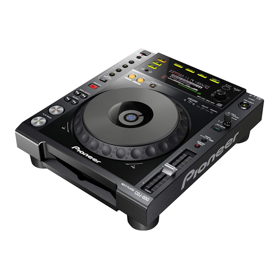
Page 10: Panel Facilities
2.3 PANEL FACILITIES CDJ-850... - Page 11 CDJ-850...
- Page 12 CDJ-850...
-
Page 13: Basic Items For Service
Before shipping out the product, be sure to clean the following positions by using the prescribed cleaning tools. Position to be cleaned Name Part No. Remarks Pickup lenses Cleaning liquied GEM1004 Refer to "9.5 SLOTIN MECHA SECTION". Cleaning paper GED-008 CDJ-850... -
Page 14: Pcb Locations
2..DFLB ASSY 2..JFLB ASSY DWX3154 1..SLOTIN MECHA ASSY DXA2206 1..TM ASSY-S (VTM091) DXX2616 ∗ The service part of DFLB Assy (DWX3152) is supplied with KSW1 Assy (DWS1422) and SLD1 Assy (DWS1423). (There assemblies are connected with the jumper wires.) CDJ-850... - Page 15 CDJ-850...
-
Page 16: Block Diagram
GNDD USBA_D_N 2 USBA_D_N V+7R6_D CMPX ASSY USBA_D_P 3 USBA_D_P V+7R6_D GNDD 4 GNDD GNDD GNDD 5 GNDD GNDD (DWX3153) D20PDY0510E GNDD CN2005 JH2201 Pitch=2.0mm GNDM 52147-0510 51048-0500 Length=100mm V+7R6_M Vertical Vertical Parallel Jumper Vertical CN2004 Wire KM200N A13 CDJ-850... - Page 17 V K N 1 2 5 2 - A 1 V+5_USB 2 USBA_D_N USBA ASSY 3 USBA_D_P 4 GNDD 5 GNDD (DWX3156) 20PDY0510E JH2201 tch=2.0mm 51048-0500 ngth=100mm Vertical arallel Jumper J A 2 2 0 1 D K B 1 1 0 6 - 1 CDJ-850...
-
Page 18: Signal Block Diagram
15 11 MUTE ROUT IC301 CIRCUIT CLK11M CN2005 IC303 IC302 OP AMP DACBCLK, JH2201 DACBCLK, DACBCLK V+5_USB USBA_D_N USBA_D_P X103 IC105 JA2003 X-tal Buffer USB Type A 16.9344 CONNECTOR JA2003 JA2002 JA2001 USBA AUDIO OUT CONTROL USB Type B CONNECTOR CDJ-850... - Page 19 LOOPIN_SW MAIN_XBUSY KEY,LED LOOPOUT_SW MAIN_XRST RELOOP_SW IN_LED VDET OUT_LED PWR_ON RELOOP_LED PNL_XMUTE JH1302 ENC_1 ENC_2 POWER DETECT ENC_SW CIRCUIT V1001 S1018 XOUT PNL_XRST DATA FL ROTARY SW X1001 X-tal IC1004 CN1601 15.975 MHz RESET IC USBA ASSY PSWB ASSY CDJ-850...
-
Page 20: Power Supply Block Diagram
REGULATOR 10V→5V VDET V+5_A IC303 V-10_A OP AMP IC2003 USB OVER CURRENT PROTECT (1A) POWER DETECT CIRCUIT MUTE CIRCUIT CN2005 JH2201 V+5_USB JA2003 USB Type A CONNECTOR JA2003 JA2002 JA2001 USBA AS AUDIO OUT CONTROL USB Type B CONNECTOR CDJ-850... - Page 21 FET SW V+38 IC1004 RESET IC PWR_ON V+6R6 VR1301 TOUCH/RELEASE IC1006 V+6R6 V+12 V+6R6 DCDC 12V→6.6V SLD1 ASSY V+12_EUP V+12 V+12 PWR_ON VDET JH1302 POWER DETECT CIRCUIT V+3R3_EUP V1001 S1018 ROTARY SW DATA FL CN1601 USBA ASSY PSWB ASSY CDJ-850...
-
Page 22: Diagnosis
TOC If the pickup is reading the position memory will be program area, it will jump located after the unit is to the TOC area. turned ON. The first track is searched for. Playback (Muting OFF) CDJ-850... -
Page 23: Troubleshooting
If the PWR_XON is "H", poor connection or Q2021 may be defective. CMPX Assy Check the V+12 voltage of CN2001-pins If the voltage is not output, POWER SUPPLY Assy 10.13 VOLTAGES Power failure POWER 4 and 5. may be defective. SUPPLY Assy CDJ-850... - Page 24 If no signal is output, the PANEL CPU (IC1007) may communication line of FL in the JFLB Assy. 10.14 be defective. • J_SCLK WAVEFORMS Signal errors JFLB Assy If output signal is no problem, JOG FL (V1801) may • J_SO be defective. • J_LAT • J_BK CDJ-850...
- Page 25 SPEED ADJUST VR (VR1301) may be defective. Defective PANEL If the symptom persists after the above Check a mounting state of PANEL CPU (IC1007). [10] Basic operation DFLB Assy CPU (IC1007) corrections, If the mounting is OK, the IC1007 may be defective. check of CPU/DSP CDJ-850...
- Page 26 Adjust Plate is reached, shavings 8.4 JOG Dial washer, gear, or Rotation Load Adjustment.” from the worn-out washer may have increased the cam plate Rotation Load friction. Replace the washer, load gear, and cam plate Adjustment. with new ones, then reassemble. CDJ-850...
- Page 27 MAIN CPU (IC101), the signal line or the Signal error Check the waveform of the control signal 10.14 MAIN Assy peripheral devices may be defective. Defective part lines (CONT1/CONT2). WAVEFORMS If the input signal can be recognized, the MAIN CPU (IC103) may be defective. CDJ-850...
- Page 28 If the symptom persists after the above procedures described in “6. SERVICE MODE.” 6. Service mode — Service mode corrections, check operations of the CD If the CD drive functions improperly, drive in Service mode. see “[8] SERVICE MODE” in this section. CDJ-850...
- Page 29 MAIN Assy (V+7R6_M, V+5R6_M, VREF1R65, BLOCK DIAGRAM VREF1R65 is produced at the Servo IC (IC201). V+3R3_S) If this voltage is not output, check the mounting status of the IC201. If it is properly mounted, then the part may be defective. CDJ-850...
- Page 30 Check the waveforms of TSCK, TSI, displayed on the See “[1-3] “E-8709” is displayed on the DATA FL DFLB Assy — PNL_BUSY, TSO, and MAIN_BUSY, DATA FL display display after startup“ for details. MAIN Assy check the voltages of V+3R3 and V+1R2. after startup CDJ-850...
- Page 31 "H". — PANEL CPU the TSCK signal is not output, the PANEL CPU • 16 MHz OSC circuit: Oscillation circuit for 10.15 EACH (IC1007) system clock. (IC1007) may be defective. SIGNAL LEVEL • TSCK(IC1007-pin 37): Communication clock signal output. CDJ-850...
-
Page 32: Diagnosis Of The Pickup Assy
5.3 DIAGNOSIS OF THE PICKUP ASSY CDJ-850... -
Page 33: Connection Check With The Pc
USB Composite Device Under “Sound, video and game controllers” USB Audio Device Human Interface Devices HID-compliant device USB Human Interface Device A communication check may be easily performed if connection is made with Device Manager displayed on the PC screen. CDJ-850... -
Page 34: About Power Supply Monitoring
P2004 DEK1095-: Protection against excess current for V+12_EUP and against excess voltage for its subsequent circuits Diagnostic procedure 1 Unplug the AC power cord. 2 Check for any error, such as short-circuiting or defective parts, in the circuits subsequent to the protector. 3 Repair the detective part. 4 Replace the protector. CDJ-850... -
Page 35: Service Mode
Mode for firmware updating. Two modes (one for updating using a USB memory device and one for updating using a CD-ROM) are provided. Refer to the “8.3 UPDATING OF THE FIRMWARE.” 6.2 ABOUT THE DEVICE OF CDJ-850 Device Name Function Part No. -
Page 36: Details On Service Mode
TEMPO SLIDER VOLUME : If a TEMPO slider knob is moved to the - side, a bar At the encoder rotation display will increase. *: JOG, ENCODER, VOLUME Display the data for the touched controls in the third line. At the TOUCH/RELEASE VOLUME rotation CDJ-850... - Page 37 Display pattern changes(Refer to the display pattern of BROWSE_FL) TAG TRACK ROTARY SELECTOR (SW) ENC PUSH ROTARY SELECTOR (FWD ROTATE) ENCODER g MARK Right movement (Max 8 points) ROTARY SELECTOR (REV ROTATE) ENCODER g MARK Left movement (Max 8 points) CDJ-850...
- Page 38 (In DATA_FL, it becomes all putting out lights except the case of all-points light.) Lattice pattern All turning off All turning on [2] Check mode of the load of JOG dial Refer to the "8.4 JOG DIAL ROTATION LOAD ADJUSTMENT." CDJ-850...
- Page 39 USB writing error Writing to the USB storage device failed. — — COMMUNICATION ERROR E-8709 Communication between the panel CPU and the main CPU failed. E-9101 A mechanical error (timeout) was generated during loading/unloading of a disc. LOADING TIMEOUT CDJ-850...
- Page 40 The product does not judge whether they are inferior goods at the time of service. Eject A disc is ejected. Mode Change If the MASTER TEMPO button is pushed into player operation mode, MASTER TEMPO LED will light up, and it will shift to the below-mentioned "test operation mode." CDJ-850...
- Page 41 *To start up the unit in Test mode in steps, input the commands in the following order: "Servo All Off," "Focus On," then “Spindle Kick, Tracking On." [6] Updating of the firmware Refer to the "8.3 UPDATING OF THE FIRMWARE." CDJ-850...
-
Page 42: Disassembly
• Rear view Front (3) Remove the control panel section. Control panel section Diagnosis MAIN Assy (4) Disconnect the 21P FFC from control panel CN2003 section. 21P FFC Screw tightening order The other screws are random order. MAIN Assy CDJ-850... - Page 43 "OPEN". CNCT Assy SHORT SW SHORT OPEN S2501 (2) Disconnect the four flexible cables. JINT Assy (3) Remove the earth lead wire by removing the one screw. (BPZ30P080FNI) CN2303 CN2304 CN2302 CN2301 Eart lead wire CDJ-850...
- Page 44 Float spring G5 Float spring G5 (7) Remove the SLOTIN MECHA section. SLOTIN MECHA section Direction of the dampers when attaching them When attaching the dampers, place them so that their projections (large) face front. Projection (large) to the front Damper CDJ-850...
- Page 45 • Be careful to the installation places. • Confirm it by viewing. This boss is not installation position. [2] SLOTIN MECHA Assy (1) Disconnect the one flexible cable. SLOTIN MECHA SLMB (2) Unhook the four hooks. Assy Assy CN1701 CDJ-850...
- Page 46 Side B [3] TM Assy-S (VTM091) Pickup (1) Short-circuit two positions of figure solodering. (short) Note: After working, connect the flexible cable, then remove the soldered joint (open). • Rear view (2) Unhook the four hooks. TM Assy-S (VTM091) CDJ-850...
- Page 47 Note on the float rubber installation Pole of the float base 05 Assy Hook ×2 Cleaning the pickup lens Before shipment, be sure to clean the pickup lens, using the following cleaning materials: Cleaning liquid : GEM1004 Cleaning paper: GED-008 Pickup lens CDJ-850...
- Page 48 Arrangement of the FFC • Pickup FFC • Spindle motor FFC Spindle motor Tape • Stepping motor FFC Stepping motor Stepping motor Pickup CNCT Assy • 5P FFC SLMB Assy 5P FFC CDJ-850...
- Page 49 About details of Adjustment etc., refer to the Adjust plate “8.4 JOG DIAL ROTATION LOAD ADJUSTMENT”. PCB Assemblies Position PSWB Assy High (SLD1 Assy) High (DFLB Assy) Low (KSW1 Assy) Low (DFLB Assy) DFLB Assy KSW1 Assy SLD1 Assy Jumper wire Jumper wire CDJ-850...
- Page 50 (4) Unhook the three hooks. (5) Remove the JOG section. JOG section (6) Remove the three screws. (DBA1265) (7) Remove the SW ring. SW ring ×3 Note: Be careful not to lost SW spring. SW spring CDJ-850...
- Page 51 5. When making a connection, be sure to first release the lock of the connector then securely relock the connector after making the connection. JOG holder M Pasting position of the SW cushion HH48/2 SW cushion HH48/2 (×9) Sheet SW CDJ-850...
-
Page 52: Each Setting And Adjustment
LIBRARY CREATOR LIBRARY/FOLDER DYW1796 Flash ROM IC101 MAIN UTILITY setting HISTORY NAME HISTORY TAGLIST NAME TAG LIST AUTO STANDBY OFF/ON VERSION No. — TIME MODE TIME/REMAIN AUTO CUE ON/OFF DYW1796 Flash ROM IC101 MAIN Statuses of keys JOG MODE CDJ/VINYL CDJ-850... -
Page 53: Updating Of The Firmware
3 Starts updating when USB memory is inserted. The FL is displayed the following screen during update. At the same time, a current version and rewriting version are displayed. 4 Following screen will be displayed if update is completed, the power is shut off once, then the unit back on. CDJ-850... - Page 54 When the power supply has been turned off on the way, subsequent normal operation becomes impossible. When the error code of "E-7024" is displayed, the recovery mode operates when performing the update procedure mentioned above again, and update is performed. In this case, please perform the recovery by USB memory. CD-ROM cannot be used. CDJ-850...
-
Page 55: Jog Dial Rotation Load Adjustment
Remove the screw fixing the adjust plate, then screw it into the hole corresponding to the value (-1, -2, -3, -4, +1, +2 or +3) for a load to be added: -1, -2, -3, -4 : To decrease the load +1, +2, +3 : To increase the load CDJ-850... -
Page 56: Exploded Views And Parts List
Screws adjacent to b mark on product are used for disassembly. For the applying amount of lubricants or glue, follow the instructions in this manual. (In the case of no amount instructions, apply as you think it appropriate.) 9.1 PACKING SECTION FLXJ only KXJ5 only AXJ5 only SYXJ8 only CDJ-850... - Page 57 See Contrast table (2) NSP 13 License Key Label DRW2402 NSP 14 License Key Label Assy DXA2190 (2) CONTRAST TABLE CDJ-850/SYXJ8, CUXJ, FLXJ, KXJ5 and AXJ5 are constructed the same except for the following: CDJ-850 CDJ-850 CDJ-850 CDJ-850 CDJ-850 Mark...
-
Page 58: Exterior Secion
9.2 EXTERIOR SECION Refer to "9.3 CONTROL PANEL SECTION". SLMB CN1701 Stepping Motor Pickup Assy Spindle Motor Refer to "9.5 SLOTIN MECHA SECTION". CDJ-850... - Page 59 18 Power Supply Stay DNH2936 19 Main PCB Stay DNH2937 NSP 20 USB Stay DNH2938 (2) CONTRAST TABLE CDJ-850/SYXJ8, CUXJ, FLXJ, KXJ5 and AXJ5 are constructed the same except for the following: CDJ-850 CDJ-850 CDJ-850 CDJ-850 CDJ-850 Mark Symbol and Description...
-
Page 60: Control Panel Section
9.3 CONTROL PANEL SECTION JFLB CN1802 Refer to "9.4 JOG DIAL SECTION". Tape CMPX CN2003 CDJ-850... - Page 61 38 • • • • • 39 • • • • • 40 Screw BPZ30P080FNI ∗ The service part of DFLB Assy (DWX3152) is supplied with KSW1 Assy (DWS1422) and SLD1 Assy (DWS1423). (There assemblies are connected with the jumper wires.) CDJ-850...
-
Page 62: Jog Dial Section
9.4 JOG DIAL SECTION Lubricating oil (ZLB-HFD1600) Lubricating oil (ZLB-HFD1600) Lubricating oil (ZLB-HFD1600) Lubricating oil (GYA1001) Lubricating oil (GYA1001) DFLB CN1002 CDJ-850... - Page 63 22 JOG Dial A DNK5357 23 Roller A Assy DXB2010 24 JOG Stay Assy DXB2015 25 • • • • • 26 • • • • • 27 Screw (FE) DBA1265 28 Screw BPZ20P100FTC 29 Screw BPZ30P080FNI 30 Screw IPZ20P060FTC CDJ-850...
-
Page 64: Slotin Mecha Section
Dyfree Dyfree (GEM1036) (GEM1036) Lubricating oil (GYA1001) Lubricating oil (GYA1001) Cleaning liquid (GEM1004) CNCT Cleaning paper (GED-008) CN2501 JINT CN2304 JINT CN2301 Note: The TM Assy-S (VTM091) is supplied only in assembly form, not as a single parts. Tape CDJ-850... - Page 65 30 Screw BPZ20P060FTC 31 Spacer POR (T3) DEB1566 32 Vessel Cushion (C) DEC2854 33 Vessel Cushion T DEC3349 34 Vessel Cushion U DEC3350 35 Front Sheet DED1132 36 Float Base 05 Assy DXB2068 37 Floating Rubber VEB1351 38 Binder ZCA-SKB90BK CDJ-850...
-
Page 66: Schematic Diagram
(TS) V+5P GNDS GNDS V+5P GNDS LD780 GNDS SHORT GNDS OPEN GNDS SHORT SW CN1701 S1701 VKN1265-A DSG1017-A LPS2 LPS2 LPS1 LPS1 S1702 GNDD DSG1017-A ZWNN1007G28-9-06A L=60mm WHITE GNDD LOADING MOTOR ASSY-S DXX2615 ZWNN1007G28-8-06A L=60mm GRAY SLMB ASSY (DWS1425) CDJ-850... - Page 67 : Stepping Motor Signal Route Indicated in Capacity/Voltage(V) GND for Digital GNDD unless otherwise noted. u F , p (LO) : Loading Motor Signal Route GND for Servo *RESISTORS GNDS Indicated in 5% tolerance GND for Frame unless otherwise noted. k CDJ-850...
-
Page 68: Main Assy (1/4)
C 1 0 8 V S S 1 V D D 3 3 3 0 p / 5 0 K4S561632J-UC75 GNDD ADRS5 ADRS5 ADRS6 ADRS6 ADRS7 ADRS7 V+3R3 ADRS8 ADRS8 ADRS9 ADRS9 ADRS10 ADRS10 ADRS12 ADRS13 DQMLL SDRAM(256M) GNDD CONTROL ADRESS CDJ-850... - Page 69 D S S 1 1 9 3 - A DBG_TxD 33.00MHz DBG_RxD UART GNDD R 1 7 1 J T A G _ X R S T V+3R3_B V+3R3B OSCILLATOR GNDD F R O M O W N S H E E T GNDD GNDD CDJ-850...
-
Page 70: Main Assy (2/4)
V+3R3_S INSW R 2 7 6 GNDD GNDS INSIDE GNDS The > mark found on some component parts indicates the importance of the safety factor of the part. Therefore, when replacing, be sure to use parts of identical designation. CDJ-850... - Page 71 : Loading Motor Signal Route Notes is No Mount (STBY) : Waveform Measuring Point CKSSYB***K F CKSRYB***K F : Voltage Measuring Point CCSRCH***J F CCSSCH***J F : Signal Level Point CEHVAW***M F RS1/16SS***J RS1/16SS****F RS1/16SS****D RS1/10SR****F RS1/10SR***J 1/4W RS1/4SA***J VCG1063A-T 1000pF/50V CDJ-850...
-
Page 72: Main Assy (3/4)
R 3 0 5 2 2 k DATA_L (DA) GNDD DACLRCK (DA) (DA) DACDATA DACBCLK CLK11M Notes is No Mount (STBY) CKSSYB***K F CKSRYB***K F CCSRCH***J F CCSSCH***J F CEHVAW***M F RS1/16SS***J RS1/16SS****F RS1/16SS****D SR F RS1/10SR****F RS1/10SR***J 1/4W RS1/4SA***J VCG1063A-T 1000pF/50V CDJ-850... - Page 73 ( G N D D ) Q 3 0 3 R T 3 T 2 2 M GNDD GNDD V-AUDIO (V-11_A) GNDD CPU_AUDIO 1:12B : Analog Audio Signal Route (DA) : Audio Data Signal Route : Waveform Measuring Point : Signal Level Point CDJ-850...
-
Page 74: Main Assy (4/4)
GNDD Q414 R487 LTA124EUB Q415 V+12_IJO GNDD 2SA1576A(QR) R491 Q413 PWR_ON LTC124EUB 11C;8A GNDD Q411 GNDD LSC4081UB(QR) R461 GNDD V+12_IJO V+12_IJO V-10_A GNDD Notes V+1R2 V+1R25 R448 R431 R420 R443 Q405 Q408 HN1C01FU(YGR) HN1C01FU(YGR) GNDD GNDD SR F 1/4W CDJ-850... - Page 75 RS1/16SS****F RS1/16SS****D SR F RS1/10SR****F The > mark found on some component parts RS1/10SR***J indicates the importance of the safety factor of the part. 1/4W Therefore, when replacing, be sure to use parts RS1/4SA***J of identical designation. VCG1063A-T 1000pF/50V CDJ-850...
-
Page 76: Cmpx (1/2) And Usba Assys
L2001 GNDD V+12_EUP GND for Analog P2001 CTF1488-A V+12 GNDA V+12 GND for Servo GNDM PWR_XON GNDD GNDM CAUTION - FOR CONTINUED PROTECTION AGAINST RISK OF FIRE, REPLACE WITH SAME TYPE No.466.375 MFD. BY LITTELFUSE INC. FOR P2004. GNDD CDJ-850... - Page 77 EP05Q06 V+10_A V+10_A V-11_A V-10_A V-11 GNDD GNDD GNDD GNDD The > mark found on some component parts indicates the importance of the safety factor of the part. Therefore, when replacing, be sure to use parts of identical designation. CDJ-850...
-
Page 78: Cmpx Assy (2/2)
CAUTION - FOR CONTINUED PROTECTION AGAINST RISK OF FIRE, The > m unless otherwise noted. u F , p indicates REPLACE WITH SAME TYPE No.466.500 MFD. BY *RESISTORS Indicated in 5% tolerance Therefore unless otherwise noted. k LITTELFUSE INC. FOR P2003. of identic CDJ-850... - Page 79 R2054 USBB_N USB CONNECTOR USBB_P B Type GNDD GNDD The > mark found on some component parts indicates the importance of the safety factor of the part. Therefore, when replacing, be sure to use parts of identical designation. GNDD CDJ-850...
-
Page 80: Dflb Assy
DSS1166-A CN1002 15.975MHz GNDD VKN1273-A *CAPACITORS GNDD Indicated in Capacity/Voltage(V) unless otherwise noted. u F , p V+3R3_EUP V+38 IC1004 *RESISTORS R1179 Indicated in 5% tolerance unless otherwise noted. k RESET CHIP JUMPER CN1802 VOUT BD45302G RESET IC GNDD CDJ-850... - Page 81 V+6R6_FL V+3R3_SW GNDD GNDA R1179 Q1025 CHIP LTC124EUB JUMPER The > mark found on some component parts indicates the importance of the safety factor of the part. Therefore, when replacing, be sure to use parts of identical designation. GNDD CDJ-850...
-
Page 82: Ksw1 And Ksw2 Assys
V S G 1 0 2 4 - A S 1 4 0 5 V S G 1 0 2 4 - A S 1 4 0 6 V S G 1 0 2 4 - A C 1 4 0 3 GNDD CDJ-850... - Page 83 Q 1 2 0 6 (RED) GNDD R 1 2 0 3 L T C 1 2 4 E U B Vf=2.2V If=1.5mA W=3.2mW REV_LED 1 . 5 k D 1 2 0 7 D 1 2 0 2 GNDD CDJ-850...
-
Page 84: Jflb And Jogb Assys
V+3R3 The > mark found on some component parts : Waveform Measuring Point indicates the importance of the safety factor of the part. Therefore, when replacing, be sure to use parts : Voltage Measuring Point of identical designation. CDJ-850... - Page 85 GNDD TRIG DISCH GNDD RS1/4SA***J THRES CKSRYB RESET CONT C1821 CCSRCH 100p CH TLC555IP CEHAR C1822 CEHAZL GNDD GNDD V+3R3_SW JOGB ASSY (DWX3155) PC1901 CN1901 SEDS-7573 52151-0410 R1901 VLED JOG2 JOG1 GND1 R1902 V+3R3_SW GNDD Vf=1.52V If=11.8mA(typ If=16mA) GNDD CDJ-850...
-
Page 86: Sld1, Pswb And Sld2 Assys
R T 2 C N 1 5 0 1 5 2 1 4 7 - 0 4 1 0 GNDD C N 1 6 0 1 5 2 1 4 7 - 0 3 1 0 L M N CDJ-850... - Page 87 SY (DWS1427) V+3R3_EUP V+3R3_EUP *CAPACITORS Indicated in Capacity/Voltage(V) ADCT unless otherwise noted. u F , p *RESISTORS TEMPO SLIDER Indicated in 5% tolerance unless otherwise noted. k A D I N 3.3V NOTES means STANDBY RS1/10SR***J CKSRYB CEJQ GNDA GNDA CDJ-850...
-
Page 88: Power Supply And Acin Assys
T3.15AL 250V 220p D3SBA60 SFPL-52 R114 D101 0.22 220p C101 SCK15057M 0.0022 EXT41641-687C B2P3-VH-LF RC101 470k FME-220A C102 0.001 330/25V /25V 470k SARS04 MTZJ24B FMV13N60ES BAS21-03W KTA1666 100k EG01C SSC6210A UDZS20B BAS21-03W BAS21-03W 0.33 0.01 0.001 0.001 MTZJ30B PS2571-1 0.0022 CDJ-850... - Page 89 FME-220A C102 R105 PS2571-1 C103 R111 L101 /25V D102 /25V UDZS5.1B R106 R103 2.2k TCB-064 C104 R104 3.3k Q102 0.22 CN2001 R108 KTC3875 100k R113 Z101 STANDBY-CONTROL IN R112 4.7k RX102 R107 Q101 KRC122S D103 L103 UDZS15B GNDD FBR07VA121 CDJ-850...
-
Page 90: Voltages
POWER SW is OFF) checked V+27 25.7 to 28.4 V IC1803, R1837-1839 V+38 34.2 to 41.8 V D1802, D1803, V1001 VFDP2R7_F1 AC2.7 V, DC7.1 to 7.8 V IC1802, Q1807, T1801, D1801, Q1803 VFDP2R7_F2 7.1 to 7.8 V D1801, Q1803 CDJ-850... -
Page 91: Waveforms
V: 1.0 V/div. H: 1 S/div. DISC EJECT IC103 - pin 72 (DSPDREQ) Foot of R193 (TSO) IC201 - pin 37 (RFO_TP) V: 1.0 V/div. H: 20 μS/div. V: 1.0 V/div. H: 200 μS/div. V: 500 mV/div. H: 500 nS/div. CDJ-850... - Page 92 V1801 - pin 25 (J_BK) V1801 - pin 26 (J_LAT) V1801 - pin 24 (J_DSO) V: 1.0 V/div. H: 200 μS/div. V: 1.0 V/div. H: 200 μS/div. V: 1.0 V/div. H: 200 μS/div. V: 1.0 V/div. H: 200 μS/div. CDJ-850...
-
Page 93: Each Signal Level
H (3.3 V): Release SERVO DSP reset SRVRST L (0 V): SERVO DSP reset H (3.3 V): After the disc insertion DRVMUTE1, 2 L (0 V): The disc non-insertion 1.65 V: In normal (At the acceleration of the start-up is SPIN around 3V.) CDJ-850... -
Page 94: Pcb Connection Diagram
17.GNDS 24.FR 9.GNDS 19.D CNCT 20.E C2502 1.FR 21.VCC DWX3151- 2.FD 8.PD 14.A 22.VREF 3.TR 9.LD780 15.B 23.F 4.TD 10.GNDS 16.VRF 24.GNDS 17.SW1_ 5.NC 11.VR780 6.GNDS 12.VRCOM DVD/CD 7.LD650 13.VR650 18.C CN2501 (DNP2602-C 09SD PICKUP ASSY A B C CDJ-850... - Page 95 Note that only the printing of the pin numbers is wrong but that that of the signal SHORT OPEN S2501 names is correct. When performing diagnosis, be sure to interpret the pin numbers [[ G ]] of the connector in reverse (enumerated right to left). A30C5/C7 CNCT DWX3151- /J (DNP2602-C) CDJ-850...
- Page 96 SIDE B SLMB ASSY DWS1425- /J SLMB CN1701 WHITE GRAY [[ G ]] 1.LPS2 2.LPS1 3.GNDD 4.LO+ SLOTSW 5.LO- SLOTSW ADD SOLDER CN1701 (DNP2601-C) CN2303 JINT ASSY CN2305 GNDS V+5M GNDF CNCT ASS A B C CDJ-850...
- Page 97 SIDE B CN1701 1.LPS2 2.LPS1 3.GNDD 4.LO+ 5.LO- N1701 CN2304 N2303 CN2301 CN2302 (DNP2602-C) CNCT ASSY CN2502 CN2501 (DNP2602-C) CDJ-850...
-
Page 98: Main Assy
C137 C196 R477 C132 C133 C487 C450 C178 R507 C316 R496 R504 R179 R482 IC410 IC411 C145 R505 C446 R430 R506 Q405 R499 R419 R448 R431 KN402 Q408 C452 R420 R417 IC103 IC410 IC411 IC403 IC401 IC205 Q405 Q408 CDJ-850... - Page 99 R134 R135 R136 C143 C217 A-S2 C138 V+3R3B C215 C142 C137 A-S1 C275 C211 AGCRF C201 R201 R276 R292 C212 R177 R240 R241 R179 C261 C145 C222 C223 C202 C260 C204 GNDS KN404 (DNP2600-C) IC103 IC105 IC404 IC104 IC201 CDJ-850...
- Page 100 R142 R238 C224 KN102 AWRC IC101 R237 R236 C220 L207 C219 R235 L208 R226 L209 C216 L210 R229 L211 R224 L212 C203 L213 L214 C191 L225 C478 C477 IC204 IC206 Q104 Q107 IC203 IC408 IC102 IC405 Q201 Q109 IC101 CDJ-850...
- Page 101 C454 R495 C507 R494 Q402 R487 R412 R411 R501 R425 D406 D405 Q404 R502 R410 (DNP2600-C) Q412 IC409 Q101 IC102 IC107 Q102 IC101 Q303 Q302 Q301 IC301 IC302 IC303 IC402 IC406 Q413 Q414 Q411 Q410 Q415 Q406 Q404 Q402 CDJ-850...
-
Page 102: Cmpx And Usba Assys
18.VDET 17.GNDD 16.MAIN_XMUTE 15.GNDD IC2003 14.MAIN_XRST 13.TSI 12.MAIN_XBUSY 11.TSO 10.PNL_XBUSY 9.GNDD 8.TSCK 7.GNDD 6.V+5R6 5.V+5R6 4.GNDD Q2034 R2084 3.GNDD 2.V+12_EUP 1.GNDD C2099 1.V+12_EUP V+12_ 2.GNDD 3.PNL_XRST V+12 4.PNL_CNVSS 5.TSCK V+12 6.TSI PWR_ 7.PNL_XBUSY GNDD 8.TSO L2006 9.PWR_ON GNDM CN2001 CDJ-850... - Page 103 R2047 (DNP2602-C) CN2004 CN401 27.USBA_D_P 6.USBA_D_N 25.GNDD 4.USB_CODETFLG 23.GNDD 22.USB_VBUSON 21.GNDD 0.PWR_ON 19.GNDD 8.VDET 17.GNDD 6.MAIN_XMUTE 15.GNDD 4.MAIN_XRST 13.TSI 2.MAIN_XBUSY 11.TSO 0.PNL_XBUSY 9.GNDD 8.TSCK 7.GNDD 6.V+5R6 5.V+5R6 4.GNDD 3.GNDD 2.V+12_EUP 1.GNDD C2099 V+12_ V+12 V+12 PWR_ GNDD GNDM CN2001 CDJ-850...
- Page 104 (DNP2602-C) CN2004 PNL_CN 27.USBA_D_P 25.GNDD 26.USBA_D_N 23.GNDD 24.USB_CODETF 21.GNDD 22.USB_VBUSO 20.PWR_ON 19.GNDD 18.VDET 17.GNDD 16.MAIN_XMU 15.GNDD 14.MAIN_XRST 13.TSI 12.MAIN_XBUS 11.TSO 10.PNL_XBUSY 9.GNDD 8.TSCK 7.GNDD 6.V+5R6 5.V+5R6 4.GNDD 3.GNDD 1.GNDD 2.V+12_EUP USBA_D_P MAIN_XMUTE PNL_CNVSS V+12_ V+12 V+12 PWR_ GNDD GNDM CDJ-850...
- Page 105 5.TSCK 2.V+12_EUP 2.PNL_XBUSY 3.TSI USBA_D_P 1.TSO USBA_D_N GNDD USB_CODETFLG (DNP2602-C) PWR_ON USB_VBUSON MAIN_XMUTE VDET MAIN_XRST V+12_EUP MAIN_XBUSY V+5R6 PNL_CNVSS V+12 V+12 PNL_XRST TSCK 1.V+12_EUP V+12_EUP 2.GNDD PNL_XBUSY V+12 3.PNL_XRST V+12 4.PNL_CNVSS 5.TSCK PWR_XON 6.TSI GNDD 7.PNL_XBUSY 8.TSO GNDM 9.PWR_ON CDJ-850...
-
Page 106: Dflb Assy
Production Code J1088 J1033 TIME J1018 S1004 J1054 J1072 J1073 J1027 J1034 IC1006 J1081 J1051 J1059 J1002 D1012 J1003 J1083 J1093 DFLB DWX3152- /J RELOOP J1086 S1005 S1006 LOOP IN LOOP OUT J1043 IC1006 J1064 J1069 J1060 J1031 J1007 CDJ-850... - Page 107 J1075 J1042 J1099 1033 J1102 J1012 1054 J1021 J1013 J1027 J1028 J1067 J1105 J1004 J1035 J1037 J1080 J1030 J1091 MEMORY J1029 DELETE < CALL CALL > S1014 S1013 J1036 152- /J J1006 J1063 CN1002 CONTACT SIDE (DNP2601-D) CN1002 CN1802 CDJ-850...
- Page 108 GNDD GNDD GNDD GNDD 2.GNDD GNDD 3.V+38 GNDD 4.GNDD 5.JOG1 6.JOG2 V+3R3_EUP 7.JOG_SW 8.J_DSO V+38 9.J_BK 10.J_SCLK V+12 11.J_LAT CALL > IC1001 12.GNDD 13.V+3R3_SW DELETE < CALL GNDD CONTACT SIDE (DNP2601-D) CN1002 NOTE: The encircled numbers denote measuring point. CDJ-850...
- Page 109 GNDD GNDD Q1006 GNDD 1.GNDD Q1005 GNDD 2.V+12_EUP Q1004 3.GNDD 4.V+12 5.V+12 6.GNDD 7.VDET LOOP OUT LOOP IN V+12 8.PNL_XMUTE 9.PWR_ON 10.MAIN_RST 11.USB_STOP 12.MAIN_BUSY V+12_EUP 13.PNL_RST 14.GNDD 15.PNL_CNVSS 17.TSCK 16.GNDD 18.GNDD 19.TSI 20.PNL_BUSY 21.TSO V+12 GNDD GNDD GNDD GNDD CDJ-850...
-
Page 110: Ksw1 And Ksw2 Assys
J1209 J1207 J1213 J1203 TRACK SEARCH J1217 J1231 J1204 J1210 S1403 S1404 J1228 KSW2 J1208 J1206 DWS1426- /J SEARCH J1218 S1405 S1406 J1219 J1225 J1212 J1216 S1401 J1227 J1401 J1230 BEAT J1402 SELECT PLAY S1402 (DNP2601-C) JH1201 (DNP2601-C) JH1201 CDJ-850... - Page 111 Q1203 GNDD KSWB GNDD Q1204 DWS1426- /J Q1401 Q1205 PLAY_LED R1401 KEY2_B Q1205 C1401 1.V+6R6 2.GNDD 3.CUE_LED 4.CUE_SW V+6R6 5.PLAY_LED 6.PLAY_SW 7.KEY2_B V+6R6 GNDD GNDD [[ G ]] R1413 R1404 R1403 Q1402 C1402 R1412 PLAY Q1206 (DNP2601-C) (DNP2601-C) JH1201 CDJ-850...
-
Page 112: Jflb And Jogb Assys
J1808 J1816 IC1802 J1802 IC1803 J1809 J1801 C1831 J1831 J1806 J1827 J1825 J1832 J1817 J1828 V1801 J1821 Q1801 C1801 DWX3154- /J JFLB Q1802 (DNP2601-C) IC1802 Q1801 Q1803 Q1802 IC1803 JOGB ASSY 4.GNDD 3.V+3R3 JOGB 2.JOG1 1.JOG2 DWX3155- CN1901 (DNP2601-C) CDJ-850... - Page 113 GNDD VFDP2R7_F2 Q1804 V+12 V+27SW V+12 Q1805 DWX3154- /J GNDD JFLB Q1806 V+3R3_SW V+3R3_SW [[ G ]] GNDD 4.GNDD 3.V+3R3_SW 2.JOG1 1.JOG2 (DNP2601-C) Q1808 Q1807 Q1805 Q1804 Q1806 JOGB ASSY DWX3155- /J C1901 R1901 R1902 C1902 R1903 JOGB (DNP2601-C) CDJ-850...
-
Page 114: Sld1, Pswb And Sld2 Assys
EUP_LED S1601 Production Code J1322 CN1601 J1317 J1319 J1308 SLD2 ASSY J1304 J1323 J1314 CN1601 J1303 J1318 J1310 J1306 J1307 J1320 J1321 J1316 J1503 J1502 J1315 TOUCH/RELEASE J1501 J1311 D1302 J1302 J1301 J1309 J1312 (DNP2601-C) L M N (DNP2601-C) CDJ-850... - Page 115 CN1601 TCH/REL VINYL_LED MT_LED GNDD GNDA ADCT ADIN V+6R6 V+3R3_EUP 1.ADCT 2.ADIN 3.GNDA D1305 4.V+3R3_EUP TOUCH/RELEASE V+3R3_EUP ADD SOLDER GNDA V+3R3_EUP Q1303 Q1304 Q1305 V+3R3_EUP GNDA GNDA V+6R6 4.V+3R3_EUP 3.GNDA 2.ADIN 1.ADCT Q1301 Q1301 (DNP2601-C) (DNP2601-C) L M N CDJ-850...
-
Page 116: Power Supply And Acin Assys
11.8 POWER SUPPLY and ACIN ASSYS SIDE A SIDE A POWER SUPPLY ASSY AC POWER CORD ACIN ASSY JA2401 LIVE NEUTRAL DWX3158- /J DWX3173- /J PURPLE BLUE ACIN (DNP2601-C) CDJ-850... - Page 117 SIDE B SIDE B POWER SUPPLY ASSY ACIN ASSY JA2401 ADDITIONAL SOLDER NEUTRAL LIVE DWX3158- /J DWX3173- /J [[ G ]] ADDITIONAL SOLDER (DNP2601-C) CDJ-850...
-
Page 118: Pcb Parts List
IC 302 PCM1742KE IC 303 RNB4580F CAPACITORS > IC 401 BA33BC0WFP C 2501,2505 CKSRYB104K16 > IC 402,408 S-1170B33UC-OTS C 2502,2503 CKSRYB103K50 C 2504,2506 DCH1201 > IC 403,404 BD00KA5WFP > IC 405,406 NJM2872BF05 > IC 409 BD9326EFJ Q 101,405,408 HN1C01FU CDJ-850... - Page 119 R 468 RS1/16SS1102D C 306,310,313,314 CKSSYB104K10 R 470,471,483 RS1/4SA0R0J C 315,411,412 CEHVAW220M6R3 R 472-474,480,481 RS1/10SR330J C 316,445,451,468 CCSRCH102J50 R 484,502 RS1/16SS1002F C 317,400,418,430 VCG1063 R 501 RS1/16SS1202F C 319,321,403,407 CKSSYB104K10 Other Resistors RS1/16SS###J C 322,323,405,406 CEHVAW101M6R3 C 326,327 CCSRCH181J50 CAPACITORS CDJ-850...
- Page 120 JA 2001 USB CONNECTOR DKN1237 C 2204 CCSRCH102J50 JA 2002 JACK VKB1243 JA 2003 PIN JACK (2P) AKB7181 DFLB ASSY CN 2001 CONNECTOR B6B-XH-A CN 2002 27P CONNECTOR VKN1258 SEMICONDUCTORS CN 2003 21P CONNECTOR VKN1252 > IC 1001 NJM2392M CDJ-850...
- Page 121 Q 1807 RHP020N06 C 1016 CEHAS101M10 D 1801 UDZS6R8(B) C 1021,1038,1040,1043 CCSRCH470J50 D 1802,1803,1805,1806 RB160M-60 C 1022,1023 CCSRCH220J50 D 1804 UDZS10(B) C 1024 CCSRCH560J50 D 1807 1SS355 C 1025,1028 CCSRCH270J50 D 1808,1809 RB160M-60 C 1027,1078 CCSRCH221J50 C 1030 CEHAZL221M6R3 CDJ-850...
- Page 122 DKP3889 RESISTORS > JP 2401 CONNECTOR ASSY 2P DKP3870 All Resistors RS1/10SR###J MISCELLANEOUS PC 1901 PHOTO INTERRUPTER SEDS-7573 ACIN ASSY (DWX3173) MISCELLANEOUS CAPACITORS > JA 2401 AC INLET DKP3891 C 1901,1902 CKSRYB103K50 > JP 2401 CONNECTOR ASSY 2P DKP3870 CDJ-850...