Sony CDX-F5000 Service Manual
Fm/am compact disc player
Hide thumbs
Also See for CDX-F5000:
- Operating instructions manual (52 pages) ,
- Installation/connections (4 pages) ,
- Operating & installation instructions (2 pages)
Table of Contents
Advertisement
CDX-F5000/FW500
SERVICE MANUAL
Ver 1.1 2004. 05
• The tuner and CD sections have no adjustments.
AUDIO POWER SPECIFICATIONS
POWER OUTPUT AND TOTAL HARMONIC DISTORTION
23.2 watts per channel minimum continuous average power into
4 ohms, 4 channels driven from 20 Hz to 20 kHz with no more
than 5% total harmonic distortion.
CD player section
Signal-to-noise ratio
120 dB
Frequency response
10 – 20,000 Hz
Wow and flutter
Below measurable limit
Tuner section
FM
Tuning range
87.5 – 107.9 MHz
Antenna terminal
External antenna connector
Intermediate frequency 10.7 MHz/450 kHz
Usable sensitivity
9 dBf
Selectivity
75 dB at 400 kHz
Signal-to-noise ratio
67 dB (stereo),
69 dB (mono)
Harmonic distortion at 1 kHz
0.5% (stereo),
0.3% (mono)
Separation
35 dB at 1 kHz
Frequency response
30 – 15,000 Hz
AM
Tuning range
530 – 1,710 kHz
Antenna terminal
External antenna connector
Intermediate frequency 10.7 MHz/450 kHz
30 µV
Sensitivity
Power amplifier section
Outputs
Speaker outputs
(sure seal connectors)
Speaker impedance
4 – 8 ohms
Maximum power output 52 W × 4 (at 4 ohms)
Sony Corporation
9-961-429-02
2004E04-1
e Vehicle Company
© 2004. 05
Published by Sony Engineering Corporation
Model Name Using Similar Mechanism
CD Drive Mechanism Type
Optical Pick-up Name
SPECIFICATIONS
General
Outputs
Inputs
Tone controls
Power requirements
Dimensions
Mounting dimensions
Mass
Supplied accessories
Design and specifications are subject to change without
notice.
FM/AM COMPACT DISC PLAYER
US Model
CDX-F5000/FW500
Canadian Model
CDX-R3000/RW300
MG-611XA-186//K
KSS1000E
Audio outputs terminal (rear/sub switchable)
Power antenna relay control terminal
Power amplifier control terminal
Telephone ATT control terminal
Remote controller input terminal
BUS control input terminal
BUS audio input terminal
Antenna input terminal
Low: ±10 dB at 60 Hz (XPLOD)
Mid: ±10 dB at 1 kHz (XPLOD)
High: ±10 dB at 10 kHz (XPLOD)
12 V DC car battery
(negative ground)
Approx. 178 × 50 × 177 mm
× 2 × 7 in.) (w/h/d)
(7
1/8
Approx. 182 × 53 × 161 mm
× 2
× 6
(7
in.) (w/h/d)
1/4
1/8
3/8
Approx. 1.2 kg
(2 lb. 10 oz.)
Parts for installation and connections (1 set)
Front panel case (1)
Card remote commander RM-X115
CDX-F5000
1
Advertisement
Table of Contents

Related Manuals for Sony CDX-F5000


Summary of Contents for Sony CDX-F5000
- Page 1 Speaker outputs (sure seal connectors) Speaker impedance 4 – 8 ohms Maximum power output 52 W × 4 (at 4 ohms) FM/AM COMPACT DISC PLAYER Sony Corporation 9-961-429-02 2004E04-1 e Vehicle Company © 2004. 05 Published by Sony Engineering Corporation...
- Page 2 NE REMPLACER CES COMPOSANTS QUE PAR DES PIÈCES REPLACE THESE COMPONENTS WITH SONY PARTS WHOSE SONY DONT LES NUMÉROS SONT DONNÉS DANS CE MANUEL PART NUMBERS APPEAR AS SHOWN IN THIS MANUAL OR OU DANS LES SUPPLÉMENTS PUBLIÉS PAR SONY.
- Page 3 CDX-F5000/FW500 Notes on CD-Rs (recordable CDs)/CD-RWs (rewritable UNLEADED SOLDER CDs) Boards requiring use of unleaded solder are printed with the lead This unit can play the following discs: free mark (LF) indicating the solder contains no lead. (Caution: Some printed circuit boards may not come printed with the lead free mark due to their particular size.)
-
Page 4: Table Of Contents
CDX-F5000/FW500 TABLE OF CONTENTS 1. GENERAL Location of Controls (CDX-F5000) ........5 Location of Controls (CDX-FW500) ........5 Connections (CDX-F5000) ............. 6 Connections (CDX-FW500) ............ 7 2. DISASSEMBLY 2-1. Sub Panel Assy (CD) ............9 2-2. CD Mechanism Block ............9 2-3. -
Page 5: General
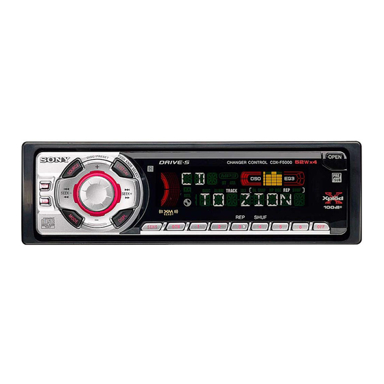
CDX-F5000/FW500 SECTION 1 GENERAL This section is extracted from instruction manual. (CDX-F5000) (CDX-FW500) Location of controls Location of controls Refer to the pages listed for details. Refer to the pages listed for details. OPEN OPEN SEEK SEEK SEEK SEEK SHUF... -
Page 6: Connections (Cdx-F5000)
CDX-F5000/FW500 Connections (CDX-F5000) CDX-F5500 only CDX-F5500 uniquement Source selector (not supplied) Supplied with the CD/MD changer Sélecteur de source Fourni avec le changeur de CD/MD (non fourni) Supplied with XA-C30 XA-C30 Fourni avec le XA-C30 AUDIO OUT REMOTE FRONT BUS AUDIO IN from car antenna à... -
Page 7: Connections (Cdx-Fw500)
CDX-F5000/FW500 Connections (CDX-FW500) CDX-FW550 only sólo CDX-FW550 Source selector (not supplied) Supplied with the CD/MD changer Selector de fuente Suministrado con el cambiador de CD/MD (no suministrado ) Supplied with XA-C30 XA-C30 Suministrado con el XA-C30 AUDIO OUT REMOTE FRONT... -
Page 8: Disassembly
CDX-F5000/FW500 SECTION 2 DISASSEMBLY Note : This set can be disassemble according to the following sequence. 2-1. SUB PANEL ASSY (CD) (Page 9) 2-2. CD MECHANISM BLOCK (Page 9) 2-10. SERVO BOARD 2-3. MAIN BOARD 2-4. CHASSIS (T) SUB ASSY... -
Page 9: Sub Panel Assy (Cd)
CDX-F5000/FW500 Note : Follow the disassembly procedure in the numerical order given. 2-1. SUB PANEL ASSY (CD) 3 two claws 2 two claws CNP802 1 two screws (+PTT 2.6 x 6) 5 sub panel assy (CD) 2-2. CD MECHANISM BLOCK... -
Page 10: Main Board
CDX-F5000/FW500 2-3. MAIN BOARD 1 three screws (+BTT) 2 two screws (+PTT 2.6 x 8) 3 MAIN board 2-4. CHASSIS (T) SUB ASSY 4 claw 2 two screws (+P 1.7 x 2.2) 1 two screws (+P 1.7 x 2.2) 6 chassis (T) sub assy... -
Page 11: Roller Arm Assy
CDX-F5000/FW500 2-5. ROLLER ARM ASSY 3 washer (1.1 – 2.5) 5 roller arm assy 4 worm wheel (RA) 2 spring (RAR) 1 spring (RAL) 2-6. CHASSIS (OP) ASSY qa chassis (OP) assy 0 compression spring (damper) lever (D) 4 washer... -
Page 12: Optical Pick-Up
CDX-F5000/FW500 2-7. OPTICAL PICK-UP 2 chucking arm sub assy 5 claw 1 tension coil spring (CHKG) 7 optical pick-up 6 main shaft 4 rack (SL) 3 screw (+B 1.4 x 5) 2-8. SL MOTOR ASSY (M902) 1 screw (+P 1.4 x 1.8) -
Page 13: Le Motor Assy (M903)
CDX-F5000/FW500 2-9. LE MOTOR ASSY (M903) 8 screw 0 woam (LEB) assy (+M 1.7 x 2.5) 9 bearing (LEB) 2 washer qa screw (+M 1.7 x 2.5) qf two toothed lock screws 3 gear (LE1) (+M 1.4 ) lever (D) -
Page 14: Diagrams
CDX-F5000/FW500 SECTION 3 DIAGRAMS 3-1. IC PIN DESCRIPTIONS • IC1 µPD63712GC-8EU-A (RF AMP, DIGITAL SERVO, DIGITAL SIGNAL PROCESSOR) (SERVO BOARD) Pin No. Pin Name Pin Description Laser diode ON/OFF control signal output (L: laser OFF, H: laser ON) Dimmer monitor input from optical pick-up laser diode. - Page 15 CDX-F5000/FW500 Pin No. Pin Name Pin Description LRCK Not used. (Connect to LRCKIN in this set) DVDD — Power supply pin (+3.3 V) Focus servo drive PWM signal output (+) FD– Focus servo drive PWM signal output (–) Tracking servo drive PWM signal output (+) TD–...
- Page 16 CDX-F5000/FW500 • IC801 MB90477PF-G-168-BNDE1 (SYSTEM CONTROL) (MAIN BOARD (2/2)) Pin No. Pin Name Pin Description Audio mute control signal output 2 to 4 — Not used in this set. (Open) BEEP Beep signal output to power amp IC VOL ATT...
- Page 17 CDX-F5000/FW500 Pin No. Pin Name Pin Description TEL ATT TEL ATT signal output ACC IN Accessory power supply detect signal input SIRCS Remote control signal (infrared rays) input RAM BU Not used in this set. (Fixed at “L”.) TEST IN...
-
Page 18: Block Diagram -Cd Section
CDX-F5000/FW500 3-2. BLOCK DIAGRAM — CD SECTION — • R-ch is omitted due to same as L-ch. • Siganal Path : CD PLAY DETECTOR MAIN 77 AGCI AGCO 71 RFI 69 ASY LOUT CD-L SECTION (Page 19) ROUT R-CH RF AMP,DIGITAL SERVO,... -
Page 19: Block Diagram -Main Section
CDX-F5000/FW500 3-3. BLOCK DIAGRAM — MAIN SECTION — ELECTRONIC VOLUME IC401 R-CH AUDIO IN R-CH CD-L PJ401 9 C2 SECTION OUTS1 R-CH 8 C1 (Page 18) REAR OUTS2 R-CH AUDIO OUT R-CH TUX601 POWER AMP MUTE (TUNER UNIT) IC100 Q407... -
Page 20: Block Diagram -Display Section
CDX-F5000/FW500 3-4. BLOCK DIAGRAM — DISPLAY SECTION — 3-5. CIRCUIT BOARDS LOCATION SYSTEM CONTROL LCD DRIVER IC801 (3/3) IC901 SERVO board ROTARY SENSOR board LCD901 ENCODER SEG10 RE901(1/2) LIQUID LCD SO SPEAKER board SEG66 CRYSTAL LCD SCK DISPLAY COM1 PANEL... -
Page 21: Note For Printed Wiring Boards And Schematic Diagrams
CDX-F5000/FW500 3-6. NOTE FOR PRINTED WIRING BOARDS AND SCHEMATIC DIAGRAMS 3-7. WAVEFORMS THIS NOTE IS COMMON FOR PRINTED WIRING — Servo Board — BOARDS AND SCHEMATIC DIAGRAMS. — Main Board — (MODE: CD PLAY) (In addition to this, the necessary note is printed in each block.) -
Page 22: Printed Wiring Boards -Cd Mechanism Section
CDX-F5000/FW500 3-8. PRINTED WIRING BOARDS — CD MECHANISM SECTION — • Refer to page 20 for Circuit Boards Location. : Uses unleaded solder. (Page 26) -
Page 23: Schematic Diagram -Cd Mechanism Section
CDX-F5000/FW500 • Refer to page 21 for Waveforms. 3-9. SCHEMATIC DIAGRAM — CD MECHANISM SECTION — • Refer to page 29 for IC Block Diagram. TP19 TP32 TP33 R14 R15 TP31 TP20 TP30 TP29 TP14 TP21 TP28 TP27 TP26 TP13... -
Page 24: Schematic Diagram -Main Section (1/2)
CDX-F5000/FW500 3-10. SCHEMATIC DIAGRAM — MAIN SECTION (1/2) — • Refer to page 30 for IC Block Diagram. TUX601 PJ601 C435 C436 R426 PJ401 C439 C609 C443 R430 JR10 IC100 IC B/D C113 C440 R431 C424 R416 Q405 IC401 R421... -
Page 25: Schematic Diagram -Main Section (2/2)
CDX-F5000/FW500 3-11. SCHEMATIC DIAGRAM — MAIN SECTION (2/2) — • Refer to page 21 for Waveforms. (Page 24) C447 R447 C802 D702 IC803 C446 C809 R821 C801 R823 C441 C810 R822 R448 CN751 C709 C707 R834 R832 R708 R819 R709... -
Page 26: Printed Wiring Boards -Main Section
CDX-F5000/FW500 3-12. PRINTED WIRING BOARDS — MAIN SECTION — • Refer to page 20 for Circuit Boards Location. : Uses unleaded solder. PJ401 PJ601 CNP900 CNJ900 CNP901 C435 C436 R421 R418 C113 R427 R443 F901 JW111 C991 C990 C443 IC100... -
Page 27: Printed Wiring Board -Relay Section
CDX-F5000/FW500 3-13. PRINTED WIRING BOARD — RELAY SECTION — • Refer to page 20 for Circuit Boards Location. : Uses unleaded solder. (Page 28) LED931 R931 CNP902 LED930 S931 C973 (Page 26) 3-14. SCHEMATIC DIAGRAM — RELAY SECTION — CNP903... -
Page 28: Printed Wiring Board -Display Section
CDX-F5000/FW500 3-15. PRINTED WIRING BOARD — DISPLAY SECTION — • Refer to page 20 for Circuit Boards Location. : Uses unleaded solder. S902 IC951 S904 LED909 LED902 LED907 LED905 LCD901 S905 LED927 LED924 S913 S910 S917 S916 S915 S914 S912... -
Page 29: Schematic Diagram -Display Section
CDX-F5000/FW500 3-16. SCHEMATIC DIAGRAM — DISPLAY SECTION — RE901(1/2) R951 R952 R971 R973 R975 R977 R979 R981 IC951 R925 R926 R927 R928 CN901 LED910 LED914 LED918 LED922 LED926 LED920 IC905 LED902 LED905 LED908 LED913 LED917 LED921 LED925 LED919 IC901 R958... -
Page 30: Ic Block Diagrams
CDX-F5000/FW500 3-17. IC BLOCK DIAGRAMS IC2 BA5966FP-FE2 (SERVO Board) IC401 BD3808FS (MAIN Board) MUTE – – – – FADER FADER FADER FADER (0~-58, (0~-58, (0~-58, (0~-58, C BUS – -∞dB) -∞dB) -∞dB) -∞dB) GAIN+ATT LOGIC – LEVEL (+10~-29, SHIFT –... -
Page 31: Exploded Views
CDX-F5000/FW500 Ver 1.1 SECTION 4 EXPLODED VIEWS NOTE: • The mechanical parts with no reference • Color Indication of Appearance Parts The components identified by mark 0 or dotted line with mark number in the exploded views are not supplied. -
Page 32: Front Panel Section
Remark X-3384-285-1 BUTTON KIT (SVX) ASSY X-3378-390-3 CASE (PANEL) ASSY (for FRONT PANEL) X-3384-637-1 KNOB VOL (SVX) ASSY A-3220-955-A FP-CDX-F5000//C (U) (F5000) X-3384-283-1 PANEL ASSY (SVX), FRONT (F5000) A-3220-967-A FP-CDX-FW500//C (U) (FW500) X-3384-326-1 PANEL ASSY (SVX), FRONT (FW500) LCD901 1-805-456-11 DISPLAY PANEL, LIQUID CRYSTAL (F5000) -
Page 33: Cd Mechanism Section (1)
CDX-F5000/FW500 4-3. CD MECHANISM SECTION (1) (MG-611XA-186//K) not supplied not supplied (SENSOR board) not supplied not supplied Ref. No. Part No. Description Remark Ref. No. Part No. Description Remark A-3372-455-A CHASSIS (T) SUB ASSY 3-253-748-01 DAMPER (S) 3-253-729-01 SPRING (LTR), TENSION COIL 3-352-758-31 SCREW (M1.7), TOOTHED LOCK... -
Page 34: Cd Mechanism Section (2)
CDX-F5000/FW500 4-4. CD MECHANISM SECTION (2) (MG-611XA-186//K) (including M901) M902 not supplied not supplied not supplied not supplied The components identified by Les composants identifiés par une mark 0 or dotted line with mark marque 0 sont critiques pour 0 are critical for safety. -
Page 35: Cd Mechanism Section (3)
CDX-F5000/FW500 4-5. CD MECHANISM SECTION (3) (MG-611XA-186//K) M903 Ref. No. Part No. Description Remark Ref. No. Part No. Description Remark 3-262-755-01 WASHER (1.1-2.5) 3-259-467-01 BRACKET (LEM) 3-259-024-01 WHEEL (RA), WORM 3-345-648-91 SCREW (M1.4), TOOTHED LOCK A-3337-633-A ARM ASSY, ROLLER A-3372-456-A WORM (LEB) ASSY... -
Page 36: Cd Mechanism Section (4)
CDX-F5000/FW500 4-6. CD MECHANISM SECTION (4) (MG-611XA-186//K) Ref. No. Part No. Description Remark Ref. No. Part No. Description Remark 3-259-429-01 WHEEL (LE), WORM 3-899-829-01 WASHER (SLIT) 3-344-223-01 WASHER 3-259-032-01 GEAR (LE2) 3-259-470-01 GEAR (LE1) A-3372-453-A CHASSIS (M) BLOCK ASSY 3-253-755-01 LEVER (D) -
Page 37: Electrical Parts List
CDX-F5000/FW500 SECTION 5 DISPLAY ELECTRICAL PARTS LIST NOTE: • Due to standardization, replacements in • Items marked “*” are not stocked since The components identified by mark 0 or dotted line with mark the parts list may be different from the they are seldom required for routine service. - Page 38 CDX-F5000/FW500 DISPLAY MAIN Ref. No. Part No. Description Remark Ref. No. Part No. Description Remark < TRANSISTOR > R974 1-216-809-11 METAL CHIP 1/10W (F5000) Q501 8-729-901-81 TRANSISTOR 2SC2412K-T-146-R R975 1-216-806-11 METAL CHIP 1/10W (FW500) < RESISTOR > R975 1-216-809-11 METAL CHIP...
- Page 39 CDX-F5000/FW500 MAIN Ref. No. Part No. Description Remark Ref. No. Part No. Description Remark C106 1-124-234-00 ELECT 22uF C809 1-124-584-00 ELECT 100uF C107 1-124-233-11 ELECT 10uF C810 1-125-701-11 DOUBLE LAYERS 0.047F 5.5V C109 1-124-233-11 ELECT 10uF C812 1-107-826-11 CERAMIC CHIP 0.1uF...
- Page 40 CDX-F5000/FW500 MAIN Ref. No. Part No. Description Remark Ref. No. Part No. Description Remark D910 8-719-071-34 DIODE RB521S-30-TE61 < RESISTOR > D911 8-719-017-95 DIODE MA8180-TX D912 8-719-083-66 DIODE UDZS-TE17-18B R101 1-249-437-11 CARBON 1/4W D913 8-719-017-95 DIODE MA8180-TX R402 1-216-833-11 METAL CHIP...
- Page 41 CDX-F5000/FW500 Ver 1.1 MAIN RELAY Ref. No. Part No. Description Remark Ref. No. Part No. Description Remark R815 1-249-435-11 CARBON 1/4W R915 1-469-144-21 FERRITE, EMI (SMD) R818 1-216-809-11 METAL CHIP 1/10W R917 1-249-431-11 CARBON 1/4W R819 1-216-809-11 METAL CHIP 1/10W...
- Page 42 CDX-F5000/FW500 SENSOR SERVO Ref. No. Part No. Description Remark Ref. No. Part No. Description Remark SENSOR BOARD < IC > ************** 6-703-699-01 IC uPD63712GC-8EU-A < SWITCH > 6-705-002-01 IC BA5966FP-FE2 1-529-566-61 SWITCH, PUSH (1 KEY) (SELF) < FERRITE BEAD >...
- Page 43 CDX-F5000/FW500 Ref. No. Part No. Description Remark MISCELLANEOUS *************** 1-776-206-21 CORD (WITH CONNECTOR) (POWER) 0 153 8-820-207-02 OPTICAL PICK-UP (KSS1000E/K1RP) A-3337-640-A CHASSIS (OP) SUB ASSY (including M901) F901 1-532-877-11 FUSE (BLADE TYPE) (AUTO FUSE) 10A M902 A-3337-638-A MOTOR ASSY, SL (SLED)
- Page 44 CDX-F5000/FW500 REVISION HISTORY Clicking the version allows you to jump to the revised page. Also, clicking the version at the upper on the revised page allows you to jump to the next revised page. Ver. Date Description of Revision 2003. 12 2004.