Table of Contents
Advertisement
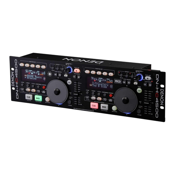
MODEL
DN-HC4500
USB MIDI/AUDIO INTERFACE & CONTROLLER
For purposes of improvement, specifications and
design are subject to change without notice.
Please use this service manual with referring to the
operating instructions without fail.
Some illustrations using in this service manual are
slightly different from the actual set.
SERVICE MANUAL
JP
PROFESSIONAL BUSINESS COMPANY
TOKYO, JAPAN
E3
E2
EK
E2A E1C E1K EUT
Ver. 2
Please refer to the
MODIFICATION NOTICE.
X0355 V.02 DE/CDM 0709
Advertisement
Table of Contents

Related Manuals for Denon DN-HC4500 Professional

Summary of Contents for Denon DN-HC4500 Professional
-
Page 1: Service Manual
Ver. 2 Please refer to the MODIFICATION NOTICE. SERVICE MANUAL MODEL E2A E1C E1K EUT DN-HC4500 USB MIDI/AUDIO INTERFACE & CONTROLLER For purposes of improvement, specifications and design are subject to change without notice. Please use this service manual with referring to the operating instructions without fail. -
Page 2: Safety Precautions
DN-HC4500 SAFETY PRECAUTIONS The following check should be performed for the continued protection of the customer and service technician. LEAKAGE CURRENT CHECK Before returning the unit to the customer, make sure you make either (1) a leakage current check or (2) a line to chassis resistance check. - Page 3 X - C O N T R O L F A D E R 1 F A D E R 2 DRIVE U S B B (For use with DENON DN-D4000/4500, BU4500 only) LINE OUT 1 LINE OUT 2 A C I N...
-
Page 4: Wire Arrangement
DN-HC4500 WIRE ARRANGEMENT If wire bundles are untied or moved to perform adjustment or parts replacement etc., be sure to rearrange them neatly as they were originally bundled or placed afterward. Otherwise, incorrect arrangement can be a cause of noise generation. - Page 5 DN-HC4500 Fasten the 6P connector with a cord holder. CX061 CX111 Fasten the P connectors with a cord holder. •Fasten the cord not to touch the trans. •Fold and fasten the cord on the CX042 side.. CX271 CX041 CX272 CX042 It coverd with TOP PANEL SUB ASSY.
- Page 6 DN-HC4500 DISASSEMBLY (Follow the procedure below in reverse order when reassembling.) 1. Top Panel Unit (1) Remove 10 side screws with washer and pull up the Top Panel Unit. Top Panel Unit (2) After pull up the Top Panel Unit, turn the back forward and then pull out the two FFC cable and two wire showed in the below drawing.
-
Page 7: Service Mode
DN-HC4500 SERVICE MODE 1. Turning on the power in the service mode (1) Turn on the power while pressing the PARAMETERS knob and the B button on either Deck 1 or Deck 2 simultaneously. The following appears on the VFD segment display section: (2) When the PARAMETERS knob is turned clockwise, the display on the lower tier of the VFD segment display section switches in the following order: "Function CHK"... - Page 8 DN-HC4500 3. Service mode function table Mode Summary Remark Turn on the power while pressing the PARAMETERS knob and the B To cancel the service Service Mode TOP button on either Deck 1 or Deck 2 simultaneously. mode, turn the power (Service Mode) Service mode starts off.
- Page 9 DN-HC4500 Mode Summary Remark Display of the status and results of the various control elements on the panel surface and external input from the side panel • PARAMETERS knob The segment on the right side of the "P" column at the upper left of the VFD segment display section toggles between white and black each time the PARAMETERS knob is pressed.
- Page 10 DN-HC4500 3.1. Switch check mode (SW Check) (1) All the VFD characters are turned off. The following characters are assigned to the 12 places of the VFD segment display section: Upper Lower (2) When each switch is pushed HOT1~HOT5 The numbers of the various buttons light on the track number display section and in the five places of the minutes counter display section.
-
Page 11: Midi Commands
DN-HC4500 3.3. MIDI COMMANDS (1) Data transmission The panel operation data is transmitted by MIDI command, as per the table below. Send command to PC MIDI command MIDI command items Message type items Message type Command Number Value Command Number Value SW ON : 0x9n SW ON : 0x40... - Page 12 DN-HC4500 (2) Data reception LED data reception The panel operation data is transmitted by MIDI command, as per the table below. Receive command for LED MIDI command MIDI command items Message type Notes items Message type Notes Command Number Value Command Number Value...
- Page 13 DN-HC4500 VFD symbol data reception The Various Vfd Symbols Can Be Set To On, Off Or Blinking, As Per The Table Below. Receive command for VFD Symbol MIDI command MIDI command items Message type items Message type Command Number Value Command Number Value...
- Page 14 DN-HC4500 MIDI command MIDI command items Message type items Message type Command Number Value Command Number Value ON TRG : 0x4D ON TRG : 0x4D VFD Symbol 0xBn OFF TRG : 0x4E Control Change VFD Symbol 0xBn OFF TRG : 0x4E Control Change Blink ON TRG : 0x4F Blink ON TRG : 0x4F...
- Page 15 DN-HC4500 VFD parameter data reception The time-related display and segment display can be set by MIDI command, as per the table below. Receive command for VFD Parameter MIDI command MIDI command Items Message Type Items Message Type Command Number Value Command Number Value...
- Page 16 DN-HC4500 Segment 2-6 MSB 0x13 Segment 2-6 MSB 0x13 Segment 2-7 MSB 0x14 Segment 2-7 MSB 0x14 Segment 2-8 MSB 0x15 Segment 2-8 MSB 0x15 Segment 2-9 MSB 0x16 Segment 2-9 MSB 0x16 Segment 2-10 MSB 0x17 Segment 2-10 MSB 0x17 Segment 2-11 MSB 0x18...
- Page 17 DN-HC4500 VFD segment data reception The various segments are set by 2-byte data, as per the following font code. (0x00/0x00 to 0x00/0x07 cannot be used.) Font codes for segments For the Reflex function operations corresponding to the above MIDI commands, refer to the Reflex manual.
- Page 18 DN-HC4500 4. Updating procedure 4.1. preparation (1) Connect the computer by USB cable. 4.2. procedure Turn on the device’s power in the update mode. (1) Press the BACK and SOURCE buttons simultaneously on Deck1 or Deck2. The following appears on the VFD segment display section: on Deck1 The version informationis displayed.
- Page 19 If the update file has not been loaded, “Fileis not ready.” is displayed. Update file not loaded (4) Drag and drop the update file to the ”DENON DJ Upgrade program” screen. The Load button can now be selected. The Load button can be selected.
- Page 20 DN-HC4500 (5) Press the Load button to transfer the update file. (6) The following appears on the VFD segment display section: During file transfer:on Deck1 Once file transfer is finished; > > > > (Left side: Old version, Right side: New version) Once file transfer is finished, press the OK button.
- Page 21 DN-HC4500 (7) Press the Execute button to begin updating the version. Once version updating is completed, “Version up was completed.” is displayed. The following appears on the VFD segment display section during version updating: On Deck1: Once version updating is completed: If version updating has failed, “Version up was not completed.”...
- Page 22 DN-HC4500 NOTE: • Do not turn off the set’s power or disconnect the cable connecting it to the computer during loading or version updating. Also, do not press any buttons on the set or any keys on the computer’s keyboard. •...
-
Page 23: Troubleshooting
DN-HC4500 TROUBLE SHOOTING FLOW CHART NO.1 The power cannot be turned on. See FLOW CHART No.2 <The fuse blows out.> Is the fuse normal? Is normal state restored when once unplugged Check if there is any leak or short-circuiting on the power cord is plugged again after several seconds? primary circuit component, and replace it if defective. - Page 24 DN-HC4500 FLOW CHART NO.7 -8V is not outputted. Check D903, D904 and the periphery circuit, Is the voltage of -10V or less supplied to INPUTpin and replace it if defective. of IC905? Check IC905 and the periphery circuit, and replace it if defective. FLOW CHART NO.8 +5VA is not outputted.
- Page 25 DN-HC4500 FLOW CHART NO.12 The key operation is not functioning. Are the contact point and the installation state of the Re-install the switches (S701~730, S801~830) key switches (S701~730, S801~830) normal? correctly or replace the poor switch. Check the TR701~708(TR807~814)and Does LED(LD701~736, LD801~836) light correctly ? their periphery, and service it if detective.
-
Page 26: Block Diagram
DN-HC4500 BLOCK DIAGRAM +3.3V AC Sel GND0 Main Power Power +1.2V +1.2V Jumper CX101 +1.2V DC-DC CW061 8PMINI CY061 SH7263 DND REMOTE DC-DC 16.9344MHz TRANS AC SW /25.476MHz USB De vice CX141 Audio MCLK +3.3V (MIDI/HID/Spealer) 14pin Operation cont DAC OUT D4500 cont +36V CX045... -
Page 27: Level Diagram
DN-HC4500 LEVEL DIAGRAM OUTPUT Audio SH7263 PCM178 +6.0dBV +2.78dBV 0dBFS GAIN=3.22dB GAIN=2.78dB -92dBV -95.22dBV 16bit:SNR=98dB -100dBV -100 -103.22dBV PCM1781:SNR=106dB(typ) -120 -130 -140 -150... - Page 28 DN-HC4500 SEMICONDUCTORS Only major semiconductors are shown, general semiconductors etc. are omitted to list. 1. IC’s R5S72630P200FP (IC104)
- Page 29 DN-HC4500 R5S72630P200FP Block Diagram...
- Page 30 DN-HC4500 R5S72630P200FP Terminal Function Pin No. Pin Name Symbol Function PC10/-RASU /MUTE General-purpose port Not used: OPEN -CASL SHCAS %CASL% SDRAM /CAS -RASL SHRAS %RASL% SDRAM /RAS V1SH Power supply for in Digital +1.2V DQMUU DQMUU Not used: OPEN DGND Digital GND PVSS DGND...
- Page 31 DN-HC4500 Pin No. Pin Name Symbol Function PE8/IRQ4 General-purpose port Not used: OPEN -CS4 Not used: OPEN PE4/DREQ0 General-purpose port Not used: OPEN PVSS DGND GND for I/O Digital GND PE5/DACK0 DRVDET DRVDET input Terminal Drive connection detection signal PVCC V3SH Power supply for I/O Digital +3.3V...
- Page 32 DN-HC4500 Pin No. Pin Name Symbol Function AVSS DGND Power supply for ADC/DAC Analog GND PVSS DGND GND for I/O Digital GND -WDTOVF WDT output(L active) Drives with DTA LED PVCC V3SH Power supply for I/O Digital +3.3V SSIDATA3 DATA_A Audio data For Deck1 SSIWS3...
- Page 33 DN-HC4500 Pin No. Pin Name Symbol Function PB2/IRQ2 General-purpose port Not used: 3.3k pull-up PB3/IRQ3 General-purpose port Not used: 3.3k pull-up PVCC V3SH Power supply for I/O Digital +3.3V PVCC V3SH Power supply for I/O Digital +3.3V PB4/SCL2 General-purpose port Not used: 3.3k pull-up PB5/SDA2 General-purpose port...
-
Page 34: Pin Description
DN-HC4500 W981616BH-7 (IC102) PIN DESCRIPTION PIN NUMBER PIN NAME FUNCTION DESCRIPTION 20- 24, DQ15 Address Multiplexed pins for row and column address. A0- A10 27- 32 Row address: A0- A10. Column address: A0- A7. DQ14 Bank Select Select bank to activate during row address latch time, or bank to read/write during column address latch DQ13 time. - Page 35 DN-HC4500 B6TS-04LT (IC706, 803) TB62725BFNG (IC704, 805) PCM1781 (IC802, 803) OUT2/SCK OUT1/SCS ZEROA OUT3/SD OUT0/CHG SERIAL-IN R-EXT 2 DEMP0 RESET CH0A CLOCK SERIAL-OUT 3 DEMP1 TEST1 CH0B LATCH ENABLE 4 MUTE OUT0 OUT7 MEAS CH1A 5 SCK AGND OUT1 OUT6 CH1B OUT2 OUT5...
- Page 36 DN-HC4500 2. VFD MODULE 17-BT-30GINK CGROM code table...
-
Page 37: Printed Wiring Boards
DN-HC4500 PRINTED WIRING BOARDS GU-3848 PANEL P.W.B. UNIT COMPONENT SIDE... - Page 38 DN-HC4500 FOIL SIDE...
- Page 39 DN-HC4500 GU-3849 MAIN P.W.B. UNIT FOIL SIDE COMPONENT SIDE...
-
Page 40: Component Side
DN-HC4500 GU-3850 POWER P.W.B. UNIT COMPONENT SIDE FOIL SIDE... -
Page 41: Note For Parts List
DN-HC4500 NOTE FOR PARTS LIST • Parts for which "nsp" is indicated on this table cannot be supplied. • When ordering of part, clearly indicate "1" and "I" (i) to avoid mis- supplying. • Ordering part without stating its part number can not be supplied. •... -
Page 42: Parts List Of P.w.b. Unit
DN-HC4500 PARTS LIST OF P.W.B. UNIT Parts for which "nsp" is indicated on this table cannot be supplied. The parts listed below are for maintenance only, might differ from the parts used in the unit in appearances or dimensions. Note: The symbols in the column "Remarks" indicate the following destinations. E3 : U.S.A. - Page 43 DN-HC4500 Ref. No. Part No. Part Name Remarks Q'ty New LD728,729 00D 393 9606 909 SEL6927A(TP5) LD730 00D 393 9674 915 SLR343BC4TT32 LD731 00D 393 9675 901 SLI-325DCT31W LD732-736 00D 393 9606 909 SEL6927A(TP5) LD801 00D 393 9606 909 SEL6927A(TP5) LD802 00D 393 9660 903 SELU5223C-S(RED)
- Page 44 DN-HC4500 Ref. No. Part No. Part Name Remarks Q'ty New C728,729 00D 257 0504 911 CC73CH1H240JT C730-733 CK73B1E104KT +1608 C734 CK73F1E104ZT +1608 C735,736 00D 257 0504 911 CC73CH1H240JT C740 CK73B1H222KT +1608 C741 CK73B1H332KT +1608 C744,745 CK73F1E104ZT +1608 C801,802 CK73F1E104ZT +1608 C806 CK73B1H222KT +1608...
- Page 45 DN-HC4500 GU-3849 MAIN P.W.B. UNIT ASS'Y Ref. No. Part No. Part Name Remarks Q'ty New SEMICONDUCTORS GROUP IC101 00D 262 2813 903 SN74AHCT08PW-EL2 IC102 00D 262 2855 000 16M SDRAM TSOP-8 H/W +C IC103 00D GEN 8704 DNHC4500 ROM ASSY M29W400DT55N6E IC104 00D 262 3764 006...
- Page 46 DN-HC4500 Ref. No. Part No. Part Name Remarks Q'ty New C105 CK73B1E104KT +1608 C106 CK73B1H103KT (1608) +1608 C107 CK73F1E104ZT +1608 C108,109 CK73B1E104KT +1608 C110,111 CK73B1H103KT (1608) +1608 C112 CK73F1E104ZT +1608 C113 CK73B1A105KT +1608 C114-117 CK73F1C104ZT +1005 C118 00D 254 4464 951 CE67C0J220MT(MV-B) +REF C119,120 CK73F1C104ZT...
- Page 47 DN-HC4500 Ref. No. Part No. Part Name Remarks Q'ty New C410-412 CK73B1A106KT +2125 C413 00D 257 0521 949 CK73B1A474KT C414 CK73F1E104ZT +1608 C415 CK73B1E223KT +1608 C418-423 CK73F1E104ZT +1608 C424 CK73B1E104KT +1608 C425-432 CK73B1H103KT (1608) +1608 C433 CK73B1E104KT +1608 OTHERS PARTS GROUP AS101 00D 207 0020 005 IC_SOCKET1...
- Page 48 DN-HC4500 GU-3850/E3/E2 POWER P.W.B. UNIT ASS'Y Ref. No. Part No. Part Name Remarks Q'ty New SEMICONDUCTORS GROUP IC801 00D 263 0809 006 NJM7805FA(S) IC802,803 00D 262 3692 903 PCM1781 IC804,805 00D 263 0896 909 NJM2068MD-TE1 IC901 00D 262 3765 005 BD9703T-V5 IC902 00D 262 3698 004...
- Page 49 DN-HC4500 Ref. No. Part No. Part Name Remarks Q'ty New C904 CK73F1E104ZT +1608 C905 CK73F1H103ZT +1608 C906 00D 254 4536 915 CE04W1A470MT SMG/RE3 C907-911 CK73B1E104KT +1608 C912,913 00D 253 8029 713 CK45F2EAC471KC(KX) C914 00D 256 8038 004 CF99--2EAC104M C920 00D 254 4814 006 CE04W1E472MC(KMG) C921 CK73F1E104ZT...
-
Page 50: Exploded View
DN-HC4500 EXPLODED VIEW 106 105 WARNING: Parts marked with this symbol have critical characteristics. Use ONLY replacement parts recommended by the manufacturer. -
Page 51: Parts List Of Exploded View
DN-HC4500 PARTS LIST OF EXPLODED VIEW Parts for which "nsp" is indicated on this table cannot be supplied. ASS’Y ASS’Y P.W.B. ASS'Y for which "nsp" is indicated on this table cannot be supplied. When repairing the P.W.B. ASS'Y, check the board parts table and order replacement parts. The parts listed below are for maintenance only, might differ from the parts used in the unit in appearances or dimensions. - Page 52 DN-HC4500 Ref. No. Part No. Part Name Remarks Q'ty New 00D 113 2078 103 SLIDE KNOB 00D 112 1024 100 KNOB 00D 009 0290 037 11P FFC(1.0) L=60 00D 009 0290 053 27P FFC(1.0) L=200 00D 009 0290 040 27P FFC(1.0) L=400 00D 009 0290 011 20P FFC(1.0) L=170 0RD 445 0048 003...
-
Page 53: Assembly Note
DN-HC4500 ASSEMBLY NOTE Mounting the JOG DISC JOG DISC (1) Mount SLIP MAT (B) on the JOG WHEEL SUB ASSY. SLIP MAT (B) : Ref No. 34 (The slip mat has no specific front or rear side.) JOG WHEEL SUB ASSY : Ref No. 38 (2) Next mount SLIP MAT (E). - Page 54 DN-HC4500 Folding the FFC (1) GU-3848-1 PANEL UNIT1 (00D 009 0290 040 : 27P FFC(1.0) L=400) 160mm White surface 55mm 55mm Printed surface Fold as shown on the diagram. Fold as shown on the diagram. Fold inward 35mm 35mm Fold outward Fold inward...
- Page 55 DN-HC4500 (2) GU-3848-2 PANEL UNIT2 (00D 009 0290 053 : 27P FFC(1.0) L=200 ) 100mm Fold inward Printed surface 45mm Fold outward Fold as shown on the diagram. White surface Fold as shown on the diagram.
- Page 56 DN-HC4500 (3) GU-3848-5 DISC UNIT1 / GU-3848-6 DISC UNIT2 (00D 009 0290 037 : 11P FFC(1.0) L=60) White surface Fold inward Fold inward Fold outward Place fold against the reinforcement plate. White surface Fold inward Fold as shown on the diagram. Printed surface Fold so that the reinforcement plates meet.
-
Page 57: Packing View
DN-HC4500 PACKING VIEW PARTS LIST OF PACKING & ACCESSORIES Parts for which "nsp" is indicated on this table cannot be supplied. The parts listed below are for maintenance only, might differ from the parts used in the unit in appearances or dimensions. Note: The symbols in the column "Remarks"... -
Page 58: Wiring Diagram
DN-HC4500 WIRING DIAGRAM CW041 CX041 or CX042 4 HV 3 F1 2 F2 PGND 1 PGND CX112 CY271 CX271 CY112 or CY113 CH3 DOWN 11 1 CH3A 1 SC0 2 SC1 CX111 CY111 CH2 RIGHT 9 3 CH2A 3 SC2 DGND 1 DGND SCK1... -
Page 59: Note For Schematic Diagram
DN-HC4500 NOTE FOR SCHEMATIC DIAGRAM WARNING: Parts marked with this symbol ! have critical characteristics. Use ONLY replacement parts recommended by the manufactur- CAUTION: Before returning the unit to the customer, make sure you make μ either (1) a leakage current check or (2) a line to chassis resis- tance check. -
Page 60: Schematic Diagrams
SCHEMATIC DIAGRAMS (1/5) DN-HC4500 SCHEMATIC DIAGRAMS (1/5) GU-3848-1 PANEL1 UNIT GU-3848-3 SENSOR1 UNIT GU-3848-5 DISC1 UNIT GU-3848-7 JIGU UNIT... - Page 61 SCHEMATIC DIAGRAMS (2/5) DN-HC4500 SCHEMATIC DIAGRAMS (2/5) GU-3848-2 PANEL2 UNIT GU-3848-4 SENSOR2 UNIT GU-3848-6 DISC2 UNIT...
- Page 62 SCHEMATIC DIAGRAMS (3/5) DN-HC4500 SIGNAL LINE SCHEMATIC DIAGRAMS (3 /5) GU-3849 MAIN UNIT (1/2)
- Page 63 SCHEMATIC DIAGRAMS (4/5) DN-HC4500 SCHEMATIC DIAGRAMS (4/5) GU-3849 MAIN UNIT (2/2)
- Page 64 SCHEMATIC DIAGRAMS (5/5) DN-HC4500 SIGNAL LINE SCHEMATIC DIAGRAMS (5/5) GU-3850-1 POWER UNIT...