Advertisement
S
ervice
M anua l
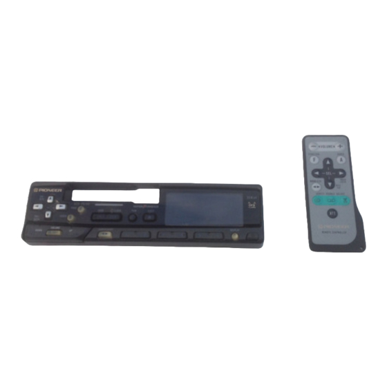
MULTI-CD CONTROL HIGH POWER CASSETTE PLAYER WITH FM/AM TUNER
KEH-P525
KEH-P5700
KEH-P5750
NOTE:
- See the separate manual CX-631(CRT1640) for the cassette mechanism description.
- The cassette mechanism assy employed in this model is one of 2L series.
- Dolby noise reduction manufactured under license from Dolby Laboratories Licensing Corporation.
"Dolby" and the double-D symbol are trademarks of Dolby Laboratories Licensing Corporation.
- This service manual does not describe the CD test mode.
For the operations in the CD test mode, refer to the CD player's Service Manual.
CONTENTS
1. SAFETY INFORMATION ...........................................2
2. EXPLODED VIEWS AND PARTS LIST......................2
3. SCHEMATIC DIAGRAM ..........................................12
4. PCB CONNECTION DIAGRAM ...............................22
5. ELECTRICAL PARTS LIST .......................................32
6. ADJUSTMENT ........................................................39
PIONEER ELECTRONIC CORPORATION
PIONEER ELECTRONICS SERVICE INC.
PIONEER ELECTRONIC [EUROPE] N.V.
PIONEER ELECTRONICS ASIACENTRE PTE.LTD. 501 Orchard Road, #10-00, Wheelock Place, Singapore 238880
C PIONEER ELECTRONIC CORPORATION 1998
• KEH-P525/X1M/UC
4-1, Meguro 1-Chome, Meguro-ku, Tokyo 153-8654, Japan
P.O.Box 1760, Long Beach, CA 90801-1760 U.S.A.
Haven 1087 Keetberglaan 1, 9120 Melsele, Belgium
X1M/UC
X1M/ES
7. GENERAL INFORMATION ......................................41
7.1 PARTS.................................................................41
7.1.1 IC ...............................................................41
7.1.2 DISPLAY ...................................................45
7.2 DISASSEMBLY ..................................................46
7.3 BLOCK DIAGRAM..............................................47
8. OPERATIONS AND SPECIFICATIONS ...................48
K-ZEM. FEB. 1998 Printed in Japan
ORDER NO.
CRT2170
X1M/UC
Advertisement
Table of Contents

Related Manuals for Pioneer KEH-P525


Summary of Contents for Pioneer KEH-P525
-
Page 1: Table Of Contents
P.O.Box 1760, Long Beach, CA 90801-1760 U.S.A. PIONEER ELECTRONIC [EUROPE] N.V. Haven 1087 Keetberglaan 1, 9120 Melsele, Belgium PIONEER ELECTRONICS ASIACENTRE PTE.LTD. 501 Orchard Road, #10-00, Wheelock Place, Singapore 238880 C PIONEER ELECTRONIC CORPORATION 1998 K-ZEM. FEB. 1998 Printed in Japan... -
Page 2: Safety Information
25249.5). When servicing or handling circuit boards and other components which contain lead in solder, avoid unprotected skin contact with the solder. Also, when soldering do not inhale any smoke or fumes produced. 2. EXPLODED VIEWS AND PARTS LIST 2.1 PACKING - KEH-P525/X1M/UC 30,31,32 Fig. 1... - Page 3 KEH-P525,P5700,P5750 NOTE: - Parts marked by “*”and ⊗ can not be supplied. - Screws adjacent to ∇ mark on the product are used for disassembly. - PACKING SECTION PARTS LIST(KEH-P525/X1M/UC) Mark No. Description Part No. Mark No. Description Part No.
- Page 4 KEH-P525,P5700,P5750 - KEH-P5700/X1M/UC,P5750/X1M/ES 17,18,19 Fig. 2...
- Page 5 KEH-P525,P5700,P5750 - PACKING SECTION PARTS LIST(KEH-P5700/X1M/UC,P5750/X1M/ES) Part No. Mark No. Description KEH-P5700/X1M/UC KEH-P5750/X1M/ES 1 Cord Assy CDE5496 CDE5496 2 Accessory Assy CEA2350 CEA2350 3 Spring CBH1650 CBH1650 4 Screw Assy CEA2351 CEA2351 5 Screw CBA1304 CBA1304 6 Polyethylene Bag CEG-127...
- Page 6 KEH-P525,P5700,P5750 2.2 EXTERIOR Fig. 3...
- Page 7 KEH-P525,P5700,P5750 (1) EXTERIOR SECTION PARTS LIST Mark No. Description Part No. Mark No. Description Part No. 1 Screw BSZ26P050FMC 46 Button( CAC5430 2 Screw BSZ30P060FMC 47 Button( CAC5432 3 Cord Assy CDE5496 48 Button(SOURCE) CAC5433 4 Spring CBH1650 49 Button(+,–)
- Page 8 KEH-P525,P5700,P5750 (2) CONTRAST TABLE KEH-P525/X1M/UC, KEH-P5700/X1M/UC and KEH-P5750/X1M/ES are constructed the same except for the following: Part No. Mark No. Description KEH-P525/X1M/UC KEH-P5700/X1M/UC KEH-P5750/X1M/ES ⊗ 20 Tuner Amp Unit CWM5671 CWM5835 CWM5835 24 Cord Assy(CN603) CDE5178 CDE5178 Not used 25 FM/AM Tuner Unit...
- Page 9 KEH-P525,P5700,P5750 2.3 CASSETTE MECHANISM MODULE Fig. 4...
- Page 10 KEH-P525,P5700,P5750 - CASSETTE MECHANISM MODULE SECTION PARTS LIST Mark No. Description Part No. Mark No. Description Part No. 1 Screw BSZ20P040FMC 31 Gear ENV1347 2 Washer CBF1037 32 Collar ENV1508 3 Washer CBF1038 33 Gear ENV1350 4 Washer CBG1003 34 Flywheel...
- Page 11 KEH-P525,P5700,P5750...
-
Page 12: Schematic Diagram
KEH-P525,P5700,P5750 3. SCHEMATIC DIAGRAM 3.1 OVERALL CONNECTION DIAGRAM (GUIDE PAGE) Note: When ordering service parts, be sure to refer to “EXPLODED VIEWS AND PARTS LIST” or “ELECTRICAL PARTS LIST”. Large size SCH diagram Guide page Detailed page... - Page 13 KEH-P525,P5700,P5750 Fig. 5...
- Page 14 KEH-P525,P5700,P5750...
- Page 15 KEH-P525,P5700,P5750 Fig. 6...
- Page 16 KEH-P525,P5700,P5750...
- Page 17 KEH-P525,P5700,P5750 Fig. 7...
- Page 18 KEH-P525,P5700,P5750 3.2 FM/AM TUNER UNIT FM/AM TUNER UNIT...
- Page 19 KEH-P525,P5700,P5750 Fig. 8...
- Page 20 KEH-P525,P5700,P5750 3.3 CASSETTE MECHANISM MODULE...
- Page 21 KEH-P525,P5700,P5750 Fig. 9 D E F...
-
Page 22: Pcb Connection Diagram
KEH-P525,P5700,P5750 4. PCB CONNECTION DIAGRAM 4.1 TUNER AMP UNIT TUNER AMP UNIT CORD ASSY NOTE FOR PCB DIAGRAMS 1. The parts mounted on this PCB include all necessary parts for several destination. For further information for respective destinations, be sure to check with the schematic diagram. - Page 23 KEH-P525,P5700,P5750 SIDE A Fig. 10 CN901 CN251...
- Page 24 KEH-P525,P5700,P5750 TUNER AMP UNIT...
- Page 25 KEH-P525,P5700,P5750 SIDE B Fig. 11...
- Page 26 KEH-P525,P5700,P5750 4.2 KEYBOARD UNIT SIDE A Fig. 12...
- Page 27 KEH-P525,P5700,P5750 SIDE B Fig. 13...
- Page 28 KEH-P525,P5700,P5750 4.3 FM/AM TUNER UNIT SIDE A Fig. 14...
- Page 29 KEH-P525,P5700,P5750 SIDE B Fig. 15...
- Page 30 KEH-P525,P5700,P5750 4.4 CASSETTE MECHANISM MODULE DECK UNIT SIDE A IC,Q ADJ VR302 IC351 IC251 HEAD ASSY Q351 Q352 VR301 Fig. 16 DECK UNIT SIDE B CN602 Fig. 17...
- Page 31 KEH-P525,P5700,P5750 PCB UNIT SIDE A Fig. 18 PCB UNIT SIDE B Fig. 19 REEL PCB Fig. 20...
-
Page 32: Electrical Parts List
KEH-P525,P5700,P5750 5. ELECTRICAL PARTS LIST NOTE: - Parts whose parts numbers are omitted are subject to being not supplied. - The part numbers shown below indicate chip components. Chip Resistor RS1/_S___J,RS1/__S___J Chip Capacitor (except for CQS..) CKS.., CCS.., CSZS..=====Circuit Symbol and No.===Part Name Part No. - Page 33 CEJA100M16 CEJAR47M50 CCSRTH9R0D50 CEJAR33M50 CCSRTH120J50 CKSQYB473K16 CKSRYB333K16 CCSRCH471J50 CKSQYB473K16 CKSRYB103K25 (KEH-P525/X1M/UC,P5700/X1M/UC) CCSRCH101J50 CCSRCH471J50 CKSRYB103K25 CKSQYB472K50 Unit Number : CWM5671(KEH-P525/X1M/UC) : CWM5846(KEH-P5700/X1M/UC) CCSRCH5R0C50 : CWM5835(KEH-P5750/X1M/ES) CKSQYB104K16 Unit Name : Tuner Amp Unit CCSRRH201J50 CKSRYB223K25 MISCELLANEOUS CKSRYB103K25 SN761027DL CCSRCH470J50 See Contrast table...
- Page 34 KEH-P525,P5700,P5750 =====Circuit Symbol and No.===Part Name Part No. =====Circuit Symbol and No.===Part Name Part No. ------ ------------------------------------------ ------------------------- ------ ------------------------------------------ ------------------------- Transistor 2SC2412K RD1/4PU103J Transistor DTC114TK RS1/10S221J Transistor 2SB1243 RS1/10S153J Diode MA152WK RS1/10S103J Diode 1SS270 RS1/10S152J Diode 1SS270 RS1/10S101J Diode...
- Page 35 KEH-P525,P5700,P5750 =====Circuit Symbol and No.===Part Name Part No. =====Circuit Symbol and No.===Part Name Part No. ------ ------------------------------------------ ------------------------- ------ ------------------------------------------ ------------------------- RS1/10S473J RS1/10S223J RS1/10S473J RS1/10S152J RD1/4PU102J RS1/10S473J RS1/10S124J RS1/10S102J RD1/4PU222J RS1/10S0R0J RS1/10S223J CAPACITORS RD1/4PU222J RS1/8S103J CEJA2R2M50 RS1/8S222J CEJA2R2M50 RD1/4PU222J CEJA1R0M50...
- Page 36 CCSQSL101J50 CKSQYB103K25 CEJA4R7M35 CEAS101M10 CKSQYB223K25 CKSQYB472K50 CKSQYB473K16 CEJA220M10 CONTRAST TABLE of TUNER AMP UNIT KEH-P525/X1M/UC, KEH-P5700/X1M/UC and KEH-P5750/X1M/ES have the same construction except for the following: Part No. Symbol and Description KEH-P525/X1M/UC KEH-P5700/X1M/UC KEH-P5750/X1M/ES FM/AM Tuner Unit CWE1467 CWE1467 CWE1486...
- Page 37 KEH-P525,P5700,P5750 =====Circuit Symbol and No.===Part Name Part No. =====Circuit Symbol and No.===Part Name Part No. ------ ------------------------------------------ ------------------------- ------ ------------------------------------------ ------------------------- Unit Number : EWM1016 CKSQYB103K50 Unit Name : Deck Unit CKSQYB103K50 CKSYB104K50 MISCELLANEOUS CKSQYB103K50 CKSQYB334K16 CXA2560Q PA2020A CKSQYB472K50 Transistor...
- Page 38 KEH-P525,P5700,P5750 =====Circuit Symbol and No.===Part Name Part No. =====Circuit Symbol and No.===Part Name Part No. ------ ------------------------------------------ ------------------------- ------ ------------------------------------------ ------------------------- RS1/4S391J Unit Number : RS1/4S391J Unit Name : PCB Unit RS1/10S472J RS1/4S391J Switch (Load) ESG1004 Switch (70µS) ESG1004 CAPACITORS...
-
Page 39: Adjustment
KEH-P525,P5700,P5750 6. ADJUSTMENT - Connection Diagram BACK UP +14.4V DC Regulated Power Supply Lch + 4Ω Lch - mV Meter (1) Oscilloscope Rch + 4Ω Rch - D u m m y A n t e n n a A n t e n n a 50Ω(37.5Ω) - Page 40 Modulation M:MONO MOD., 400Hz 30%(22.5kHz Dev.) or 400Hz 100%(75kHz Dev.) S:STEREO MOD., 1kHz, L or R=30%(20.25kHz+7.5kHz Dev.) NOTE:Before proceeding to further adjustments after switching power ON, let the tuner run for ten minutes to allow the circuits to stabilize. FM ADJUSTMENT(KEH-P525/X1M/UC,P5700/X1M/UC) FM SSG Displayed Adjustment...
-
Page 41: General Information
KEH-P525,P5700,P5750 7. GENERAL INFORMATION 7.1 PARTS 7.1.1 IC TDA7384,TDA7386 PM2006A... - Page 42 KEH-P525,P5700,P5750 - Pin Functions (PD4915A) Pin No. Pin Name Format Function and Operation ASENBO Slave power supply control output Not used ADPW A/D converter power AVSS A/D GND FIEOUT FIE ON/OFF control output FM stereo input AVREF1 (Connect to VDD)
- Page 43 KEH-P525,P5700,P5750 Pin No. Pin Name Format Function and Operation bsens Back up power sense input CLKIN Clock input Power supply Oscillator output Oscillator input Not used TESTIN Test program mode input AVDD A/D converter analogue power AVREF0 A/D converter standard voltage input...
- Page 44 KEH-P525,P5700,P5750 - Pin Functions(PD6247A) Pin No. Pin Name Function and Operation Crystal oscillator connection pin Crystal oscillator connection pin System reset MODE1,0 Dimmer select output UART output UART input REMIN Remote control reception RVER Not used Not used 13–16 KDT4–1 Key data input 17–22...
-
Page 45: Display
KEH-P525,P5700,P5750 7.1.2 DISPLAY - CAW1477 Fig. 22... -
Page 46: Disassembly
KEH-P525,P5700,P5750 7.2 DISASSEMBLY Removing the Case(not shown) 1. Remove the three screws. 2. Remove the Case. Removing the Cassette Mechanism Module (not shown) 1. Remove the four screws. 2.Disconnect the connector, and then removing the Cassette Mechanism Module. Removing the Detach Grille Assy(Fig.23) 1. -
Page 47: Block Diagram
KEH-P525,P5700,P5750 7.3 BLOCK DIAGRAM - KEH-P525/X1M/UC Fig. 25... -
Page 48: Operations And Specifications
KEH-P525,P5700,P5750 8. OPERATIONS AND SPECIFICATIONS Fig. 26... - Page 49 KEH-P525,P5700,P5750 8.1. OPERATIONS...
- Page 50 KEH-P525,P5700,P5750...
- Page 51 KEH-P525,P5700,P5750...
- Page 52 KEH-P525,P5700,P5750...
-
Page 53: Specifications
FM tuner Power source ..14.4 V DC (10.8 – 15.1 V allowable) Frequency range Grounding system ........Negative type ..87.9 – 107.9 MHz (KEH-P525/X1M/UC, P5700/X1M/UC) Max. current consumption ..10.0 A ......87.5 – 108 MHz (KEH-P525/X1M/UC) (KEH-P5750/X1M/ES) 8.5 A...