Sony SPP-A973 Service Manual
Cordless telephone sony spp-a973/ spp-a974
Hide thumbs
Also See for SPP-A973:
- Operating instructions manual (115 pages) ,
- Operating instructions manual (115 pages)
Table of Contents
Advertisement
Quick Links
SERVICE MANUAL
Ver 1.0 1999. 11
General
Frequency band (SPP-A973)
902 – 928 MHz
Frequency band (SPP-A974)
923.1 – 927.75 MHz
Base unit : 18 µW
Handset : 73 µW
Operating channel
30 channels
Dial signal
Tone, 10 PPS (pulse) selectable
Supplied accessories
AC power adaptor AC-T128 (1)
Telephone line cords (2)
Wall bracket for base phone (1)
Rechargeable battery pack BP-T23 (1)
Handset
Power source
Rechargeable battery pack BP-T23
Battery charging time
Approx. 12 hours
Battery life
Standby : Approx. 7 days
Talk
: Approx. 6 hours
Dimensions
Approx. 58 × 177 × 46 mm (w/h/d),
antenna excluded
× 7 × 1
(approx. 2
inches)
3/8
13/16
Antenna: Approx. 72 mm
(approx. 2
inches)
7/8
Mass
Approx. 270 g
(approx. 9.5 oz), battery included
MICROFILM
SPP-A973/A974
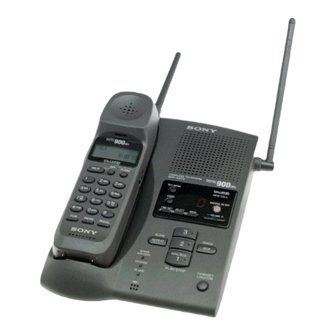
Photo: SPP-A973
SPECIFICATIONS
– 1 –
Base unit
Power source
DC 9 V from AC power adaptor
AC-T128
Battery charging time
Approx. 24 hours
Dimensions
Approx. 160 × 63 × 225 mm (w/h/d),
antenna excluded
× 2
× 8
(approx. 6
inches)
3/8
1/2
7/8
Antenna: Approx. 120 mm
(approx. 4
inches)
3/4
Mass
Approx. 585 g
(approx. 1 lb 5 oz), wall bracket excluded
Answering machine
Maximum recording time
About 15 minutes, using incorporated IC
Greeting message
Up to 90 seconds per each
Incoming and Memo message
Up to 4 minutes per message
Design and specifications are subject to
change without notice.
Notes on Chip Component Replacement
• Never reuse a disconnected chip component.
• Notice that the minus side of a tantalum capacitor may be dam-
aged by heat.
CORDLESS TELEPHONE
US Model
SPP-A973
Canadian Model
SPP-A974
Advertisement
Table of Contents

Related Manuals for Sony SPP-A973


Summary of Contents for Sony SPP-A973
- Page 1 Ver 1.0 1999. 11 Canadian Model SPP-A974 Photo: SPP-A973 SPECIFICATIONS Base unit General Frequency band (SPP-A973) Power source 902 – 928 MHz DC 9 V from AC power adaptor Frequency band (SPP-A974) AC-T128 923.1 – 927.75 MHz Battery charging time Base unit : 18 µW...
-
Page 2: Table Of Contents
Note for Replacement of the ASIC Board TABLE OF CONTENTS The ID is written in the ASIC board. When replacing the ASIC board, the U4001 on BASE MAIN board 1. GENERAL and U1001 on HAND MAIN board should be replaced together as Read This First ................ - Page 3 SECTION 1 GENERAL This section is extracted from SPP-A974’s instruction manual. – 3 –...
- Page 4 – 4 –...
- Page 5 – 5 –...
- Page 6 – 6 –...
- Page 7 – 7 –...
- Page 8 – 8 –...
- Page 9 – 9 –...
- Page 10 – 10 –...
- Page 11 – 11 –...
- Page 12 – 12 –...
- Page 13 – 13 –...
- Page 14 – 14 –...
-
Page 15: Disassembly
SECTION 2 DISASSEMBLY • The equipment can be removed using the following procedure. HANDSET CASE (REAR) RF UNIT (HS), HAND MAIN BOARD BASE UNIT BASE (BOTTOM) BASE MAIN BOARD RF UNIT (BU) BASE KEY BOARD I-TAD BOARD Note : Follow the disassembly procedure in the numerical order given. 2-1. -
Page 16: Base (Bottom)
2-3. BASE (BOTTOM) 2 BTP 3x12 6 base (bottom) 3 BTP 3x12 1 BTP 3x12 2-4. BASE MAIN BOARD 1 screws (3x30) 4 Removal the solders. 3 BTP 3x12 0 BASE MAIN board 2 BTP 3x12 5 Removal the solders. battery terminal (BU) 6 Removal the solders. -
Page 17: Rf Unit (Bu)
2-5. RF UNIT (BU) 1 BTP 3x12 3 B 2x8 2 BTP 3x12 4 RF unit (BU) 2-6. BASE KEY BOARD 2 BTP 3x12 1 BTP 3x12 3 speaker holder 7 BASE KEY board 4 B 2x6 5 B 2x6 6 Removal the solders. -
Page 18: I-Tad Board
2-7. I-TAD BOARD 3 I-TAD board BASE KEY board 1 Removal the solders. 2 BTP 3x12 – 18 –... -
Page 19: Electrical Adjustments
SECTION 3 ELECTRICAL ADJUSTMENTS 3-1. HANDSET 3-2. BASE UNIT 1. Test Mode 1. Test Mode Entry— Press “PGM” key and enter “ TEST” on keypad. Entry— Simultaneously press the “HANDSET LOCATOR” key and toggle the “DIAL MODE” switch. When in test mode, the “IN USE” Alternative entry—... -
Page 20: Diagrams
SPP-A973/A974 SECTION 4 DIAGRAMS 4-1. BLOCK DIAGRAM — BASE UNIT SECTION — ANT4001 TELESCOPIC ANTENNA RF UNIT (BU) SYSTEM CONTROL U4001 D1007-1009 T1001 HOOK DET U1002 RX AUDIO DSIN J1006 TXDATA TX DATA LINE PLL REF PLL REF RSSI APIN2... -
Page 21: Block Diagram -Handset Section
SPP-A973/A974 4-2. BLOCK DIAGRAM — HANDSET SECTION — ANT1001 HELICAL ANTENNA SYSTEM CONTROL U1001 RF UNIT (HS) PLL REF 64 PLL REF DSIN RX AUDIO U1005 TX DATA TXDATA SPEAKER RSSI ADIN2 PLL EN GPIO2/MON2 SER DATA OUT SER CLK... -
Page 22: Schematic Diagram -Base Main Section (1/2)
SPP-A973/A974 4-3. SCHEMATIC DIAGRAM — BASE MAIN SECTION (1/2) — THIS NOTE IS COMMON FOR PRINTED WIRING BOARDS AND SCHEMATIC DIAGRAMS. (In addition to this, the necessary note is printed in each block.) For schematic diagrams • All capacitors are in µF unless otherwise noted. pF: µµF 50 WV or less are not indicated except for electrolytics and tantalums. -
Page 23: Schematic Diagram -Base Main Section (2/2)
SPP-A973/A974 4-4. SCHEMATIC DIAGRAM — BASE MAIN SECTION (2/2) — • Refer to page 45 for IC Block Diagrams. – 27 – – 28 –... -
Page 24: Printed Wiring Board -Base Main Section
SPP-A973/A974 4-5. PRINTED WIRING BOARD — BASE MAIN SECTION — • Semiconductor Location Ref. No. Location D1001 D1011 D1012 D1015 D1016 D4001 D4002 D4003 Q1006 Q1008 Q4001 Q4003 U1003 U4001 U4002 U4004 U4005 – 29 – – 30 –... - Page 25 SPP-A973/A974 • Semiconductor Location Ref. No. Location D1006 D1007 D1008 D1009 D1010 Q1001 Q1007 U1001 U1002 (Page 34) (Page 38) – 31 – – 32 –...
-
Page 26: Printed Wiring Board -I-Tad Section
SPP-A973/A974 4-6. PRINTED WIRING BOARD — I-TAD SECTION — • Semiconductor Location Ref. No. Location (Q1) (Q2) (U3) ) : SIDE B (Page 38) (Page 31) – 33 – – 34 –... -
Page 27: Schematic Diagram -I-Tad Section
SPP-A973/A974 4-7. SCHEMATIC DIAGRAM — I-TAD SECTION — • Refer to page 45 for IC Block Diagrams. – 35 – – 36 –... -
Page 28: Printed Wiring Board -Base Key Section
SPP-A973/A974 4-8. PRINTED WIRING BOARD — BASE KEY SECTION — (Page 34) (Page 31) • Semiconductor Location Ref. No. Location Ref. No. Location – 37 – – 38 –... -
Page 29: Schematic Diagram -Base Key Section
SPP-A973/A974 4-9. SCHEMATIC DIAGRAM — BASE KEY SECTION — • Refer to page 45 for IC Block Diagrams. (Page 28) (Page 35) – 39 – – 40 –... -
Page 30: Printed Wiring Board -Hand Main Section
SPP-A973/A974 4-10. PRINTED WIRING BOARD — HAND MAIN SECTION — • Semiconductor Location Ref. No. Location (D1001) (D1002) (D1003) (D1004) (D1006) D1008 D1010 D1016 D1018 (D1020) D1023 D1024 D1025 D1026 D1027 D1028 (D1030) (D1031) D1032 D1033 (Q1002) (Q1004) (Q1006) (Q1007) -
Page 31: Schematic Diagram -Hand Main Section
SPP-A973/A974 4-11. SCHEMATIC DIAGRAM — HAND MAIN SECTION — • Refer to page 45 for IC Block Diagrams. – 43 – – 44 –... - Page 32 • IC Block Diagrams U1 SN74HC595ADBR (BASE KEY board) U2 PQ1R28 U1 PCD6002 (I-TAD board) 80 79 78 77 76 75 74 73 72 71 70 69 68 67 66 65 CONTROLLER PSEN 1 32KBYTE OTP P4.3 MA0 4 VSS3V2 MAIN BUS P4.5/GPC P4.4/FSI...
-
Page 33: Exploded Views
SECTION 5 EXPLODED VIEWS NOTE: • The mechanical parts with no reference • -XX and -X mean standardized parts, so • Accessories and packing materials and number in the exploded views are not supplied. they may have some difference from the hardware (# mark) list are given in •... -
Page 34: Base Unit Section
5-2. BASE UNIT SECTION ANT4001 U4003 J1002, 1005 J1003, 1004 Ref. No. Part No. Description Remark Ref. No. Part No. Description Remark * 51 A-3672-872-A BASE MAIN BOARD, COMPLETE 4-356-741-21 SCREW, TAPPING (BIND 2X8) 7-685-548-19 SCREW +BTP 3X12 TYPE2 N-S 3-038-087-01 BASE (BOTTOM) 3-041-524-01 SHIELD (F), I-TAD 3-041-534-01 FOOT, RUBBER... -
Page 35: Electrical Parts List
BASE KEY SECTION 6 ELECTRICAL PARTS LIST BASE MAIN NOTE: • Due to standardization, replacements in • Items marked “*” are not stocked since The components identified by mark 0 or dotted line with mark the parts list may be different from the they are seldom required for routine service. - Page 36 BASE MAIN Ref. No. Part No. Description Remark Ref. No. Part No. Description Remark C4014 1-162-912-11 CERAMIC CHIP 0.5PF L1006 1-408-117-00 INDUCTOR 10uH C4015 1-162-915-11 CERAMIC CHIP 10PF 0.5PF C4017 1-162-964-11 CERAMIC CHIP 0.001uF < TRANSISTOR > C4018 1-162-964-11 CERAMIC CHIP 0.001uF C4019 1-126-963-11 ELECT...
- Page 37 BASE MAIN HAND MAIN Ref. No. Part No. Description Remark Ref. No. Part No. Description Remark R4004 1-216-833-11 METAL CHIP 1/16W < VIBRATOR > R4006 1-216-813-11 METAL CHIP 1/16W R4007 1-216-813-11 METAL CHIP 1/16W X4001 1-577-269-11 VIBRATOR, CRYSTAL (18.4MHz) R4008 1-216-858-11 METAL CHIP 1.2M 1/16W...
- Page 38 HAND MAIN I-TAD Ref. No. Part No. Description Remark Ref. No. Part No. Description Remark D1003 8-719-909-90 DIODE BAV99 R1035 1-216-841-11 METAL CHIP 1/16W D1004 8-719-909-90 DIODE BAV99 R1036 1-218-292-11 RES,CHIP 1/16W D1006 8-719-047-37 DIODE BAS16 R1037 1-216-821-11 METAL CHIP 1/16W D1008 8-719-063-83 LED SML-310MTT86 (A974)
- Page 39 I-TAD Ref. No. Part No. Description Remark Ref. No. Part No. Description Remark 1-107-826-11 CERAMIC CHIP 0.1uF 1-216-845-11 METAL CHIP 100K 1/16W 1-162-921-11 CERAMIC CHIP 33PF 1-216-833-11 METAL CHIP 1/16W 1-162-921-11 CERAMIC CHIP 33PF 1-216-828-11 METAL CHIP 3.9K 1/16W 1-107-826-11 CERAMIC CHIP 0.1uF 1-216-821-11 METAL CHIP 1/16W...
- Page 40 SPP-A973/A974 Ref. No. Part No. Description Remark ACCESSORIES & PACKING MATERIALS ******************************** 1-418-739-11 ADAPTOR, AC (AC-T128) 1-528-769-11 BATTERY PACK (BP-T23) 1-696-453-21 CORD (WITH MODULAR PLUG) (LINE) (215cm) 1-696-454-11 CORD (WITH MODULAR PLUG) (LINE) (15cm) 3-012-379-11 CASE (WALL HOOK) 3-867-315-11 MANUAL, INSTRUCTION (ENGLISH,SPANISH)