Sony D-E660 Service Manual
Portable cd player
Hide thumbs
Also See for D-E660:
- Operating instructions manual (24 pages) ,
- Operating instructions manual (25 pages) ,
- Operating instructions manual (32 pages)
Table of Contents
Advertisement
D-E660/EJ610/EJ611/EJ613/EJ615/EJ616CK
SERVICE MANUAL
Ver 1.5 2001.07
With SUPPLEMENT 1
(9-927-632-81)
With SUPPLEMENT 2
(9-927-632-82)
With SUPPLEMENT 3
(9-927-632-83)
System
Compact disc digital audio system
Laser diode properties
Material: GaAIAs
Wavelength : λ= 780 nm
Emission duration: Continuous
Laser output : Less than 44.6 µW
(This output is the value measured at a distance
of 200 mm from the objective lens surface on
the optical pick-up block with 7 mm aperture. )
D-A conversion
1-bit quartz time-axis control
Frequency response
+1
20 - 20,000 Hz
dB (measured by EIAJ CP-
-2
307)
Output (at 4.5 V input level)
Line output (stereo minijack)
Output level 0.7 V rms at 47 kilohms
Recommended load impedance over 10
kilohms
Power requirements
For the area code of the model you purchased,
check the upper left side of the bar code on the
package.
• Two Sony NC-WMAA rechargeable
batteries: 2.4 V DC,
• Sony NH-WM2AA rechargeable batteries:
2.4 V DC,
9-927-632-12
Sony Corporation
Personal Audio Company
2001G0200-1
Shinagawa Tec Service Manual Production Group
© 2001.7
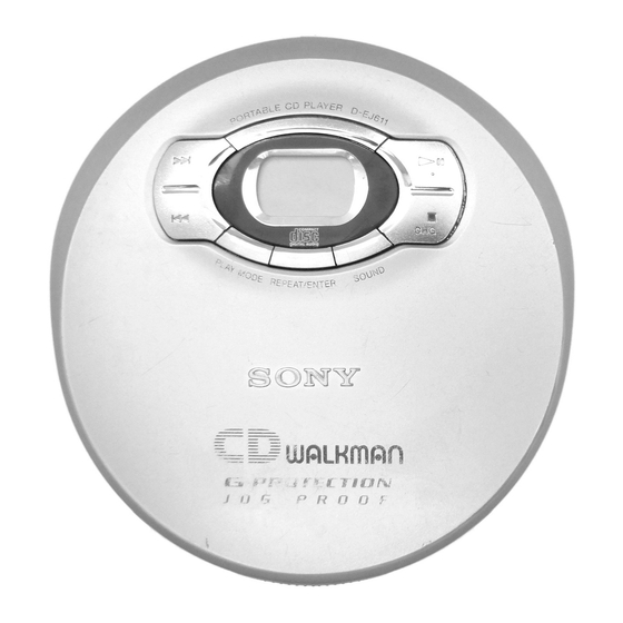
Photo : D-EJ611
SPECIFICATIONS
• Two LR6 (size AA) batteries: 3 V DC
• AC power adaptor (DC IN 4.5 V jack):
US, Canadian, C&SA model: 120 V, 60 Hz
AEP, FR, G, EE, E13 model:
220 - 230 V, 50/60 Hz
UK model: 230 - 240 V, 50 Hz
EA model: 110 - 240 V, 50/60 Hz
AUS model: 240 V, 50 Hz
JE, E33 model: 100 - 240 V, 50/60 Hz
HK model: 220 V, 50/60 Hz
AR, CH model: 220 V, 50 Hz
• Sony DCC-E245 car battery cord for use on
car battery : 4.5V DC
Battery life* (approx. hours)
(When you use the CD player on a flat and
stable surface.)
Playing time varies depending on how the CD
player is used.
When using
G-PROTECTION function
Tow NC-WMAA
(charged for about 3 hours**)
NH-WM2AA
(charged for about 4 hours**)
Tow alkaline batteries LR6
*
Measured value by the standard of EIAL
(Electronic Industries Association of Japan).
** Charging time varies depending on how the
rechargeable battery is used.
Canadian Model
Australian Model
D-EJ611/EJ615/EJ616CK
D-EJ610/EJ611/EJ613/EJ615/EJ616CK
Chinese Model
Tourist Model
Model Name Using Similar Mechanism NEW
CD Mechanism Type
Optical Pick-up Type
Operating temperature
5°C - 35°C (41°F - 95°F)
Dimensions (w/h/d) (excluding projecting
parts and controls)
Approx. 131 x 29 x 136 mm
( 5
1
/
x 1
3
/
x 5
3
/
4
16
Mass (excluding accessories)
Approx. 190 g (6.7 oz)
on
off
8
7
18
15
32
28
PORTABLE CD PLAYER
US Model
E Model
AEP Model
UK Model
D-EJ611/EJ615
D-E660
CDM-3223EBA
DAX-23E
in.)
8
– Continued on page 2 –
Advertisement
Table of Contents

Related Manuals for Sony D-E660


Summary of Contents for Sony D-E660
- Page 1 Approx. 190 g (6.7 oz) the optical pick-up block with 7 mm aperture. ) AR, CH model: 220 V, 50 Hz • Sony DCC-E245 car battery cord for use on – Continued on page 2 – D-A conversion car battery : 4.5V DC 1-bit quartz time-axis control Battery life* (approx.
-
Page 2: Table Of Contents
The AC power adaptor supplied is not intended to be serviced. Should AC 3-5. “Lid, Upper”, Switch Unit .......... 7 power adaptor cease to function in its intended manner, during the warranty period, the adaptor should be returned to your nearest Sony 4. ELECTRICAL ADJUSTMENS ....... 8 Service Center or Sony Authorized Repair Center for replacement, or after warranty period, it should be discarded. -
Page 3: Servicing Notes
SECTION 1 SERVICING NOTES Laser Diode Checking Methods NOTES ON HANDLING THE OPTICAL PICK-UP BLOCK OR During normal operation of the equipment, emission of the laser diode BASE UNIT is prohibited unless the upper panel is closed while turning ON the S801 (push switch type). -
Page 4: General
SECTION 2 This section is extracted from GENERAL instruction manual. LOCATING THE CONTROLS – 4 –... - Page 5 – 5 –...
-
Page 6: Disassembly
SECTION 3 DISASSEMBLY The equipment can be removed using the following procedure. “Motor ASSY, Turn table (Spindle) (M901)”, Cabinet (rear) sub ASSY, Main board MD ASSY Optical pick-up (DAX-23E), “Motor ASSY (Sled) (M902)” Cabinet (front) “Lid, Upper”, Switch unit Note : Follow the disassembly procedure in the numerical order given. 3-1. -
Page 7: Motor Assy, Turn Table (Spindle) (M901)
3-3. “MOTOR ASSY, TURN TABLE 3-4. “MOTOR ASSY (SLED) (M902)”, (SPINDLE) (M901)” OPTICAL PICK-UP (DAX-23E) 1 Screws 1 Screw (B 1.7x5) (B1.7x5) Cover, Gear Gear B Screw ASSY, Feed Motor ASSY (Sled) (M902) 4 Screw (P 1.4x3.5) Bracket (Shaft) Motor ASSY, Turn table (Spindle) (M901) Optical pick-up (DAX-23E) -
Page 8: Electrical Adjustments
SECTION 4 ELECTRICAL ADJUSTMENTS The CD section adjustments are done automatically in this set. Focus bias Check Condition: Precautions for Check • Hold the set in horizontal state. 1. Perform check in the order given. 2. Use YEDS-18 disc (Part No.: 3-702-101-01) unless otherwise Connection: indicated. -
Page 9: Diagrams
SECTION 5 DIAGRAMS 5-1. EXPLANATION OF IC TERMINALS IC801 (SYSTEM CONTROLLER) TMP88CM22F-MIR1-1 Pin No. Pin name Description — Ground terminal. IRRMCO — Not used (OPEN). FOKI Focus OK signal input from the digital servo processor (IC601). “L”: NG, “H”: OK AGCPWM AGC control pulse signal output terminal. - Page 10 Pin No. Pin name Description X3037 Mode select terminal for IC601. XHGOM Optical pick-up power ON/OFF control signal output terminal. “L”: ON XLAT Serial data latch pulse signal output to IC601. XSOE Serial data output enable signal output terminal. HP ATTENUATION Headphone attenuater ON/OFF signal output.
-
Page 11: Block Diagram
D-E660/EJ610/EJ611/EJ613/EJ615/EJ616CK 5-2. BLOCK DIAGRAM • Signal path. : CD – 11 – – 12 – – 13 –... -
Page 12: Printed Wiring Boards
D-E660/EJ610/EJ611/EJ613/EJ615/EJ616CK 5-3. PRINTED WIRING BOARDS Semiconductor Location Ref. No. Location D301 H-10 D302 E-16 D401 D403 B-10 D404 [MAIN BOARD] (SIDE A) [MAIN BOARD] (SIDE B) D405 J401 D406 G-12 DC IN 4.5V EXCEPT D409 C-11 US MODEL D461 US MODEL... -
Page 13: Schematic Diagram
D-E660/EJ610/EJ611/EJ613/EJ615/EJ616CK 5-4. SCHEMATIC DIAGRAM Refer to page 21 – 22 for IC Block Diagrams. Waveforms 2 Vp-p 2.1 Vp-p 1.9 µ sec 22.9 µ sec IC601 wg VOLT/DIV : 0.5 V AC IC601 ih VOLT/DIV : 0.5 V AC CLOCK TIME/DIV : 0.5 µsec... - Page 14 Ver 1.4 2000.10 SECTION 6 EXPLODED VIEWS NOTE : Ref. No. Part No. Description Remark Ref. No. Part No. Description Remark IC Block Diagrams IC601 CXD3037R • -XX, -X mean standardized parts, so they • The mechanical parts with no reference The components identified by mark 0 A-3328-742-A CABINET (REAR) SUB ASSY 4-223-605-11 LID,UPPER (BLUE) (EJ615:US,CND,AUS,...
-
Page 15: Optical Pick-Up Section (Cdm-3223Eba)
6-2. OPTICAL PICK-UP SECTION (CDM-3223EBA) M901 M902 The components identified by Les composants identifiés par une mark 0 or dotted line with mark marque 0 sont critiques pour 0 are critical for safety. la sécurité. Replace only with part number Ne les remplacer que par une pièce specified. -
Page 16: Electrical Parts List
SECTION 7 MAIN ELECTRICAL PARTS LIST NOTE : • Due to standardization, replacements in the • SEMICONDUCTORS In each case, u : µ , for example : The components identified by mark 0 parts list may be different from the parts or dotted line with mark 0 are critical uA.. - Page 17 MAIN Ref. No. Part No. Description Remark Ref. No. Part No. Description Remark C438 1-115-156-11 CERAMIC CHIP C814 1-164-505-11 CERAMIC CHIP 2.2uF C442 1-115-156-11 CERAMIC CHIP C841 1-162-970-11 CERAMIC CHIP 0.01uF C451 1-115-156-11 CERAMIC CHIP C900 1-124-234-00 ELECT 22uF C453 1-115-467-11 CERAMIC CHIP 0.22uF (EJ616CK)
- Page 18 MAIN Ref. No. Part No. Description Remark Ref. No. Part No. Description Remark L401 1-419-188-21 INDUCTOR 100uH R153 1-216-821-11 METAL CHIP 1/16W L402 1-469-525-91 INDUCTOR 10uH (US) L403 1-414-434-11 INDUCTOR 100uH R154 1-216-793-11 RES-CHIP 1/16W L404 1-469-528-91 INDUCTOR 100uH R201 1-216-813-11 METAL CHIP 1/16W L405...
- Page 19 MAIN Ref. No. Part No. Description Remark Ref. No. Part No. Description Remark R427 1-216-815-11 METAL CHIP 1/16W R628 1-216-864-11 METAL CHIP 1/16W R429 1-216-857-11 METAL CHIP 1/16W R629 1-216-833-91 RES-CHIP 1/16W R430 1-216-041-00 METAL CHIP 1/10W R630 1-216-823-91 METAL CHIP 1.5K 1/16W R431...
- Page 20 MAIN Ref. No. Part No. Description Remark Ref. No. Part No. Description Remark R824 1-216-833-91 RES-CHIP 1/16W ACCESSORIES & PACKING MATERIALS R826 1-216-841-11 METAL CHIP 1/16W ******************************** (FR) R826 1-216-849-11 METAL CHIP 220K 1/16W 1-251-696-11 CONNECTING PACK, CAR (EJ616CK) (EXCEPT US) 1-251-696-21 CONNECTING PACK, CAR (EJ616CK) R826 1-216-851-11 METAL CHIP...
- Page 21 Ref. No. Part No. Description Remark 3-868-180-81 MANUAL, INSTRUCTION (ITALIAN)(EJ610: EXCEPT FR,G/EJ611:AEP/EJ613:AEP/ EJ615:AEP) 3-868-180-91 MANUAL, INSTRUCTION (FINNISH) (EJ610: EXCEPT FR,G/EJ611:AEP/EJ613:AEP/ EJ615:AEP) 3-868-181-11 MANUAL, INSTRUCTION (TRADITIONAL CHINESE) (EJ611:E13/EJ615:E13,HK) 3-868-181-21 MANUAL, INSTRUCTION (ENGLISH) (EJ611:E13,CH/EJ615:E13,HK,CH) 3-868-181-31 MANUAL, INSTRUCTION (SIMPLIFIED CHINESE) (CH) 3-868-182-11 MANUAL, INSTRUCTION (RUSSIAN) (EJ611:EE/EJ615:EE) 3-868-182-21 MANUAL, INSTRUCTION (CZECH) (EJ611:EE/ EJ615:EE)
- Page 22 D-E660/EJ610/EJ611/EJ613/EJ615/EJ616CK – 32 –...
- Page 23 Ver 1.2 2000.09 Ver 1.4 2000.10 D-E660/EJ610/EJ611/EJ613/EJ615/EJ616CK CHANGE OF MAIN BOARD Before Change Afrer Change The main board have been changed. Ref. No. Part No. Description Part No. Description Printed wiring board and schematic diagram of new type, and changed parts list are described in this Supplement-1.
- Page 24 D-E660/EJ610/EJ611/EJ613/EJ615/EJ616CK PRINTED WIRING BOARDS Semiconductor Location Ref. No. Location Ref. No. Location D300 H-10 Q301 C-15 D301 H-10 Q302 C-16 D302 E-16 Q401 B-11 D401 Q402 D403 B-10 Q403 [MAIN BOARD] (SIDE A) [MAIN BOARD] (SIDE B) D404 Q404 J401...
- Page 25 D-E660/EJ610/EJ611/EJ613/EJ615/EJ616CK SCHEMATIC DIAGRAM Waveforms 2 Vp-p 2.1 Vp-p 1.9 µsec 22.9 µsec IC601 wg VOLT/DIV : 0.5 V AC IC601 ih VOLT/DIV : 0.5 V AC CLOCK TIME/DIV : 0.5 µsec TIME/DIV : 5 µsec LRCK 1.76 Vp-p 2.1 Vp-p...
- Page 26 MAIN MAIN MAIN MAIN ELECTRICAL PARTS LIST (Service Manual see page 26 to 31) NOTE : Ref. No. Part No. Description Remark Ref. No. Part No. Description Remark Ref. No. Part No. Description Remark Ref. No. Part No. Description Remark Ref.
- Page 27 MAIN Ref. No. Part No. Description Remark Ref. No. Part No. Description Remark R903 1-216-831-11 METAL CHIP 6.8K 1/16W 1-533-689-11 FUSE, GLASS CYLINDRICAL(DIA.5) (EJ616CK) (EJ616CK) 1-569-007-11 ADAPTOR, CONVERSION 2P (JE,E33) R904 1-216-825-11 METAL CHIP 2.2K 1/16W 1-569-008-21 ADAPTOR, CONVERSION 2P (EJ611:EA/ (EJ616CK) EJ616CK:EA) 1-756-035-11 BATTERY PACK (NC-WMAA) (E660,EJ615:...
- Page 28 D-E660/EJ610/EJ611/EJ613/EJ615/EJ616CK Ref. No. Part No. Description Remark 3-868-183-11 MANUAL, INSTRUCTION (SPANISH) (EJ616CK:AEP,E33,C&SA) 3-868-183-21 MANUAL, INSTRUCTION (ENGLISH) (EJ616CK:CND,AEP,EE,AUS,E33,C&SA,EA) 3-868-183-31 MANUAL, INSTRUCTION (FRENCH) (EJ616CK:CND,AEP) 3-868-183-41 MANUAL, INSTRUCTION (DUTCH) (EJ616CK:AEP,EE) 3-868-183-51 MANUAL, INSTRUCTION (SWEDISH) (EJ616CK:AEP) 3-868-183-61 MANUAL, INSTRUCTION (PORTUGUESE) (EJ616CK:AEP,C&SA) 3-868-183-71 MANUAL, INSTRUCTION (GERMAN)
- Page 29 D-E660/EJ610/EJ611/EJ613/EJ615/EJ616CK US Model Canadian Model SERVICE MANUAL E Model Australian Model 2000. 08 D-EJ611/EJ615/EJ616CK AEP Model D-EJ610/EJ611/EJ613/EJ615/EJ616CK UK Model Chinese Model D-EJ611/EJ615 Tourist Model D-E660 SUPPLEMENT - 2 File this Supplement with the Service Manual. Subject : KOREAN MODEL HAS BEEN ADDED FOR...
- Page 30 D-E660/EJ610/EJ611/EJ613/EJ615/EJ616CK – 2 –...
- Page 31 D-E660/EJ610/EJ611/EJ613/EJ615/EJ616CK US Model Canadian Model SERVICE MANUAL E Model Australian Model D-EJ611/EJ615/EJ616CK 2001.07 AEP Model D-EJ610/EJ611/EJ613/EJ615/EJ616CK UK Model Chinese Model D-EJ611/EJ615 Tourist Model D-E660 SUPPLEMENT - 3 File this Supplement with the Service Manual. Subject : CHANGE OF MAIN BOARD...
- Page 32 D-E660/EJ610/EJ611/EJ613/EJ615/EJ616CK CHANGE OF MAIN BOARD EXCEPT US, FR/EJ616CK The main board have been changed. Printed wiring board and schematic diagram of new type, and changed parts list are described in this Supplement-3. Refer to original service manual (9-927-632-11) and supplement-1 (9-927-632-81) previously issued for the other information.
- Page 33 D-E660/EJ610/EJ611/EJ613/EJ615/EJ616CK z PRINTED WIRING BOARDS –MAIN SECTION (1/2)– (1-679-060-13: Except US, FR/EJ616CK) Semiconductor Location MAIN BOARD (SIDE A) Ref. No. Location D401 D404 D405 D408 D410 D461 D602 D804 D805 IC302 IC310 IC402 Q402 Q403 Q404 Q409 Q500 SWITCH UNIT...
- Page 34 D-E660/EJ610/EJ611/EJ613/EJ615/EJ616CK z PRINTED WIRING BOARDS –MAIN SECTION (2/2)– (1-679-060-13: Except US, FR/EJ616CK) Semiconductor Location Ref. No. Location MAIN BOARD (SIDE B) D100 D200 J401 D300 DC IN 4.5V D301 D302 D303 D406 D409 D601 D603 D806 -1 -2 IC401 IC404...
- Page 35 D-E660/EJ610/EJ611/EJ613/EJ615/EJ616CK z SCHEMATIC DIAGRAM –MAIN BOARD (1/2) – (EXCEPT US, FR/EJ616CK) Refer to page 8 to 9 for IC Block Diagrams. Refer to page 7 for Note and Waveforms.
- Page 36 D-E660/EJ610/EJ611/EJ613/EJ615/EJ616CK z SCHEMATIC DIAGRAM –MAIN BOARD (2/2) – (EXCEPT US, FR/EJ616CK) Refer to page 8 to 9 for IC Block Diagrams. Refer to page 7 for Note and Waveforms.
- Page 37 D-E660/EJ610/EJ611/EJ613/EJ615/EJ616CK Waveforms Note: • All capacitors are in µF unless otherwise noted. pF: µµF 50 WV or less are not indicated except for electrolytics and tantalums. • All resistors are in Ω and W or less unless otherwise 2 Vp-p 2.1 Vp-p...
-
Page 38: Ic Block Diagrams
D-E660/EJ610/EJ611/EJ613/EJ615/EJ616CK IC Block Diagrams IC302 TA2120FN (EL) BIAS MUTE MUTE BIAS BEEP BEEP BIAS OUT B OUT A RF IN OCL ROUT VREF LOUT IC401 TB2119F 59 58 57 56 54 53 52 51 49 48 42 41 VREF VREF... - Page 39 D-E660/EJ610/EJ611/EJ613/EJ615/EJ616CK IC601 CXD3027R 120 119 118 117 116 115 114 113 112 111 110 109 108 107 106 105 104 103 102 101 100 99 98 97 96 95 94 93 92 91 ERROR CLOCK PCMD CORRECTOR GENERATOR SELECTOR LRCK...
- Page 40 D-E660/EJ610/EJ611/EJ613/EJ615/EJ616CK MAIN ELECTRICAL PARTS LIST (SERVICE MANUAL SEE PAGE 26 TO 31) NOTE : • Due to standardization, replacements in the • SEMICONDUCTORS In each case, u : µ , for example : The components identified by mark 0 parts list may be different from the parts or dotted line with mark 0 are critical uA..
- Page 41 D-E660/EJ610/EJ611/EJ613/EJ615/EJ616CK Ref. No. Part No. Description Remark Ref. No. Part No. Description Remark C612 1-162-962-11 CERAMIC CHIP 470PF D602 8-719-404-50 DIODE MA111-TX C613 1-162-962-11 CERAMIC CHIP 470PF D603 8-719-069-54 DIODE UDZSTE-175.1B D804 8-719-069-54 DIODE UDZSTE-175.1B C614 1-162-962-11 CERAMIC CHIP 470PF D805 8-719-069-54 DIODE UDZSTE-175.1B...
- Page 42 D-E660/EJ610/EJ611/EJ613/EJ615/EJ616CK Ref. No. Part No. Description Remark Ref. No. Part No. Description Remark Q411 8-729-429-44 TRANSISTOR XP1501-TXE R436 1-216-864-11 METAL CHIP 1/16W Q412 8-729-904-86 TRANSISTOR 2SB1197K-Q Q415 8-729-231-76 TRANSISTOR 2SC4116GL-TE85R R437 1-216-861-11 METAL CHIP 2.2M 1/16W Q416 8-729-231-76 TRANSISTOR 2SC4116GL-TE85R...
- Page 43 D-E660/EJ610/EJ611/EJ613/EJ615/EJ616CK Ref. No. Part No. Description Remark R649 1-216-833-11 METAL CHIP 1/16W R653 1-216-864-11 METAL CHIP 1/16W R654 1-216-864-11 METAL CHIP 1/16W R655 1-216-864-11 METAL CHIP 1/16W R801 1-216-845-11 METAL CHIP 100K 1/16W R802 1-216-845-11 METAL CHIP 100K 1/16W R803...
- Page 44 D-E660/EJ610/EJ611/EJ613/EJ615/EJ616CK REVISION HISTORY Clicking the version allows you to jump to the revised page. Also, clicking the version at the upper right on the revised page allows you to jump to the next revised page. Ver. Date Description of Revision 2001.07...