Advertisement
Quick Links
Download this manual
See also:
User Manual
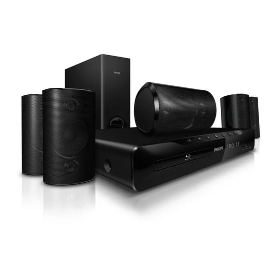
BD Home Theater System
Service
Service
Service
Service Manual
©
Copyright 2011 Philips Consumer Electronics B.V. Eindhoven, The Netherlands
All rights reserved. No part of this publication may be reproduced, stored in a retrieval system or
transmitted, in any form or by any means, electronic, mechanical, photocopying, or otherwise
without the prior permission of Philips.
Published by
RY_RL1115
Service Audio Printed in The Netherlands Subject to modification
Version 1.2
TABLE OF CONTENTS
Location Of PCB Boards............................................ 1-2
Versions Variation ...................................................... 1-2
Specifications ............................................................ 1-3
Measurement Setup .................................................. 1-6
Service Aids .............................................................. 1-7
ESD & Safety Instruction .......................................... 1-8
Lead-free Soldering Information ................................ 1-9
Setting Procedure & Repair Instructions ...................... 2
Disassembly Instructions & Service Positions .............. 3
Block & Wiring Diagram ................................................ 4
Diagram Quick Strart Guide .......................................... 5
Main Board .................................................................... 6
Power Board .................................................................. 7
BD Board........................................................................ 8
Key Board ...................................................................... 9
VFD Board .................................................................. 10
Mechanical Exploded View.......................................... 11
Revision List ................................................................ 12
1 - 1
Chapter
HTS3551
/12/51/55/78
3139 785 35712
GB
Advertisement

Related Manuals for Philips HTS3551


Summary of Contents for Philips HTS3551
- Page 1 Revision List ..............12 © Copyright 2011 Philips Consumer Electronics B.V. Eindhoven, The Netherlands All rights reserved. No part of this publication may be reproduced, stored in a retrieval system or transmitted, in any form or by any means, electronic, mechanical, photocopying, or otherwise without the prior permission of Philips.
- Page 2 1 - 2 LOCATION OF PCB BOARDS BD PCB MAIN PCB KEY PCB POWER PCB VFD PCB VERSION VARIATION: Type/Versions HTS3551 Features Output Power - 300W Voltage (220~240V) Music iLink SERVICE SCENARIO MATRIX: Type/Versions HTS3551 Board in used Main Board...
-
Page 3: Specifications
1 - 3 SPECIFICATIONS Media formats Video formats • AVCHD, BD-RE, BD-Video, DVD-Video, DVD+R/+RW, DVD-R/-RW, DVD+R/-R DL, CD-R/CD-RW, Audio CD, Video CD/ • Resolution: 1920 x 1080 pixels at • Frame rate: 6 ~ 30 frames per second. DivX (Ultra)-CD, USB storage device Audio Video codec Bit rate... -
Page 4: Main Unit
1 - 4 Video Audio Video codec Bit rate • Signal system: PAL / NTSC codec • HDMI output: 480i/576i, 480p/576p, 720p, 1080i, 1080p, 1080p24 PCM, MPEG 1, MPEG 2 20 Mbps (peak AC-3, 40 Mbps) DTS core, Audio MPEG, •... -
Page 5: Remote Control Batteries
1 - 5 Speakers • Center speaker: • Total output power: 50W RMS (30% THD) • System: full range satellite • Speaker impedance: 3 ohm • Speaker drivers: 76.2 mm (3”) full range • Frequency response: 150 Hz-20 kHz • Dimensions (WxHxD): 161 x 95 x 92 •... - Page 6 1 - 6 MEASUREMENT SETUP Tuner FM Bandpass LF Voltmeter 250Hz-15kHz e.g. PM2534 e.g. 7122 707 48001 RF Generator e.g. PM5326 S/N and distortion meter e.g. Sound Technology ST1700B Use a bandpass filter to eliminate hum (50Hz, 100Hz) and disturbance from the pilottone (19kHz, 38kHz). Use Audio Signal Disc SBC429 4822 397 30184 (replaces test disc 3)
- Page 7 1 - 7 SERVICE AIDS Service Tools: Universal Torx driver holder .........4822 395 91019 Torx bit T10 150mm ...........4822 395 50456 Torx driver set T6-T20 .........4822 395 50145 Torx driver T10 extended ........4822 395 50423 Compact Disc: SBC426/426A Test disc 5 + 5A ......4822 397 30096 SBC442 Audio Burn-in test disc 1kHz ....4822 397 30155 SBC429 Audio Signals disc .........4822 397 30184 Dolby Pro-logic Test Disc ........4822 395 10216...
- Page 8 1 - 8 WAARSCHUWING WARNING Alle IC’s en vele andere halfgeleiders zijn All ICs and many other semi-conductors are gevoelig voor electrostatische ontladingen susceptible to electrostatic discharges (ESD). (ESD). Careless handling during repair can reduce life Onzorgvuldig behandelen tijdens reparatie kan drastically.
- Page 9 • You will find this and more technical information Use only lead-free solder alloy Philips SAC305 with within the “magazine”, chapter “workshop news”. order code 0622 149 00106. If lead-free solder-paste is required, please contact the manufacturer of your For additional questions please contact your local solder-equipment.
- Page 10 000025.0 version of your home theater with the latest software version (if software updates,please visit available) on the Philips web site, and for BD-Live application and philips.com/support Software BE software update, make sure that the network router has access to the Internet and the firewall is disabled.
- Page 11 2 - 2 2 - 2 8) OSD Language setup (only for 51 version) c) Assembly Blu-ray Loader to connect “J509”,”J507”,”HA801” on Software upgrade will take 5 minutes CAUTION! the top of BD Board as shown below. a) Press “ ”...
- Page 12 2 - 3 2 - 3 REPAIR INSTRUCTIONS-part one HTS3551REPAIR CHART All fuction Power supply All function Key board AUX in is MP3 in is Coaxial in Optical in Tuner is is not working is not working is not sound is not function not sound not sound...
- Page 13 2 - 4 2 - 4 REPAIR INSTRUCTIONS-part two HTS3551 BD Board Repair block diagram(MT8550) MAIN UNIT REPAIR CHART BD function is not working Loading is not DISC All video is not output Ethernet is not starting Loading is not DISC...
- Page 14 3 - 1 3 - 1 DISASSEMBLY INSTRUCTIONS Dismantling of the VFD Board 1) Loosen 3 screws “ E “ on the top of VFD board as shown in fi gure 7. Note:In some service positions the components or copper patterns of one board may risk touching its neighbouring pc boards or metallic parts.
-
Page 15: Service Positions
3 - 2 3 - 2 SERVICE POSITIONS Service Position A - BD Board Figure 10 Dismantling of the BD Board 1) Loosen 4 screws “I” on the top of BD board as shown in fi gure 11. 2) Loosen 2 screws “J” at the back panel as shown in fi gure 12. Service Position B - Main &... - Page 16 3 - 3 3 - 3 Service Position C - Power Board Service Position E - All Board Service Position D - VFD Board...
-
Page 17: Block Diagram
4 - 1 4 - 1 BLOCK DIAGRAM MPEG Unit Part T act Switch Standb y VF D Di splay BD Vi deo(CV BS ) A/D Ke y (7Ke y) Red LED BD OPU Sanyo T RV -414VH5 CV BS out ES D REJECT OR ASA 9332 Loader 1pcs... - Page 18 4 - 2 4 - 2 WIRING DIAGRAM (Only for /55 version)
- Page 19 QUICK START GUIDE The following excerpt of the QSG/DFU serves as an introduction to the set. The complete Direction for Use can be download in the different languages from the internet site of Philips Consumer Care Center:www.support.philips.com. SUB- SUB- FRONT...
- Page 20 5 - 2 5 - 2 FRONT FRONT FRONT REAR REAR SUB- RIGHT LEFT CENTER RIGHT LEFT WOOFER FRONT FRONT FRONT REAR REAR SUB- RIGHT LEFT CENTER RIGHT LEFT WOOFER AC MAINS~ ANTENNA FM(75 Ω) AUX 1 AUX 2 COAXIAL OPTICAL AUDIO IN DIGITAL IN...
- Page 21 5 - 3 5 - 3 HDMI OUT (ARC) HDMI HDMI (ARC) MUSIC iLINK AC MAINS~ Only for /55 version...
- Page 22 5 - 4 5 - 4 HOME THEATER HOME THEATER...
- Page 23 5 - 5 5 - 5 MUSIC iLINK...
- Page 24 6 - 1 6 - 1 INTERNAL IC DIAGRAM - CS495313-CVZ Serial Serial Paraliel Debug UART GPIO Control 1 Control 2 Control 12 Ch. Audio In/ 6 Ch. SACO In 32-bit 32-bit TMR1 DSP A DSP B MAIN BOARD TMR2 S/PDIF S/PDIF 16 Ch PCM Audio Out...
- Page 25 6 - 2 6 - 2 CIRCUIT DIAGRAM C101 B1 C129 D1 C171 C1 C210 B3 C312 A2 C352 D1 C418 C4 C502 B3 C526 A3 C551 B4 C576 A4 C5991 A3 C624 D2 C667 B1 C828 D4 C9907 C4 CN9091 FB5004 IC501 B3...
- Page 26 6 - 3 6 - 3 PCB LAYOUT - TOP VIEW C103 C319 C571 FB5005 B2 R164 R304 R507 C104 C320 C572 FB722 B1 R165 R305 R508 C105 C321 C573 FB9091 C3 R166 R306 R509 C106 C322 C582 FB9092 C3 R171 R307 R514...
- Page 27 6 - 4 6 - 4 PCB LAYOUT - BOTTOM VIEW C101 A1 C557 A3 C704 C1 R270 A2 C102 A1 C558 B3 C707 A2 R271 A2 C107 A1 C559 A3 C708 B2 R272 A2 C131 A1 C560 A3 C709 A2 R273 A2 C155 A1 C561 A3...
- Page 28 7 - 1 7 - 1 INTERNAL IC DIAGRAM - AZ431 CATHODE POWER BOARD ANODE TABLE OF CONTENTS Internal IC Diagram ................7-1 Circuit Diagram .................. 7-2 PCB Layout Top View ............... 7-3 PCB Layout Bottom View ..............7-4...
-
Page 29: Circuit Diagram
7 - 2 7 - 2 CIRCUIT DIAGRAM BD901 A1 C919 C938 C954 C2 C966 C2 C981 CN905 A3 D905 D918 IC907 A2 Q905 B2 R9002 A2 R9013 A2 R9026 A2 R904 R908A B3 R919 R930 C1 R943 C3 R955 R968 R982A A1 R995... - Page 30 7 - 3 7 - 3 PCB LAYOUT - TOP VIEW BD901 A1 C908 A2 C930 A2 C946 B2 C967 A3 C984 A3 CN904 A3 CY902 B1 D910 C2 GT901 C1 J905 J911 J918 J924 J930 L904 Q901 A2 R921 A3 T901 A2 C901 A3 C917 B2...
- Page 31 7 - 4 7 - 4 PCB LAYOUT - BOTTOM VIEW C907 C2 C931 A2 C955 B3 C974 C3 D903 B2 D923 B2 Q908 B3 R9003 C1 R9012 B1 R9023 C2 R9031 C2 R9058 A1 R911A B3 R919 A1 R930 A2 R941 C1 R951 B3 R963 A2...
- Page 32 8 - 1 8 - 1 BLOCK DIAGRAM MT8550 BD boar d DDR3 BC H BD OPU Sanyo TR V- 414H05 64MB x 16 x 1 pc s ASA9332 Loader DDR3 AC H 64MB x 16 x 1 pc s SERV O NAND Fl ash 2G bit TPIC1391/...
- Page 33 8 - 2 8 - 2 Voltages for per connection pin 1. HA500--->>from BD board connect to main board 2. CN202--->>from BD board connect to USB connect PCB 4. HA801--->>from BD board connect to BD loader(SERVO use) 5. J508 --->>from BD board connect to BD loader(SERVO use) PIN NO PIN Assign Remarks...
- Page 34 8 - 3 8 - 3 Waveforms for measure point...
- Page 35 8 - 4 8 - 4 Waveforms for measure point...
- Page 36 9 - 1 9 - 1 KEY BOARD TABLE OF CONTENTS Circuit Diagram .................. 9-2 PCB Layout Top & Bottom View ............9-3...
- Page 37 9 - 2 9 - 2 CIRCUIT DIAGRAM CN701 A1 LD701 A1 Q701 A1 Q702 A2 R701 A1 R702 A1 R703 A1 R704 A2 R705 A2 R707 A2 R708 A2 R709 A1 R710 A1 R711 A1 TA701 A1 TA702 A1 TA703 A2 TA704 A2 TA705 A2 TA706 A2 TA707 A2 Press TA701 CN701 V_ (AD_ KE Y) =3.3/(1+4K 7/R701)
- Page 38 9 - 3 9 - 3 PCB LAYOUT - TOP VIEW TA707 TA706 TA705 TA704 TA703 TA702 TA701 LD701 JP15 CN701 PCB LAYOUT - BOTTOM VIEW Q701 Q702 R701 R702 R703 R704 R705 R707 R708 R709 R710 R711...
- Page 39 10 - 1 10 - 1 FTD DISPLAY PIN ASSIGNMENT VFD BOARD TABLE OF CONTENTS FTD Display Pin Assignment ............. 10-1 Circuit Diagram ................. 10-2 PCB Layout Top & Bottom View ............10-3 PIN CONNECTION...
- Page 40 10 - 2 10 - 2 CIRCUIT DIAGRAM C601 C1 C604 C1 C607 B2 C610 C1 C613 C2 C616 B3 C632 A2 C643 B2 CN602 B1 DP601 B2 FB603 A3 R601 C1 R604 C1 R607 C1 R610 C2 R613 C2 R630 A1 USB601 A2 C636 A3...
- Page 41 10 - 3 10 - 3 PCB LAYOUT - TOP VIEW C603 C614 CN602 A1 CN605 A2 JK602 A3 JP02 JP04 JP06 JP08 JP10 JP12 JP14 USB601 A3 VR601 A3 C606 CN601 A1 CN604 A3 DP601 A2 JP01 JP03 JP05 JP07 JP09 JP11...
- Page 42 11 - 1 11 - 1 Mechanical Exploded View only for /55 HDMI only for /51 only for /55 HSP140054-1080 SCREW T3.0x1.06PxL8mm NICKEL HST143084-1060 SCREW M3.0x0.5PxL6mm NICKEL 12 HST140074-1100 SCREW T3.5xL10.0xP1.41mm NICKEL PLATE 13 HSP140054-1100 SCREW T3.0x1.06PxL10mm NICKEL 17 HST143084-3060 SCREW M3x0.5PxL6mm BLACK OXIDE 21 HST143084-1080 SCREW M3.0x0.5PxL8mm NICKEL...
- Page 43 12 - 1 REVISION LIST Version 1.0 *Initial release Version 1.1 *HTS3551/78/51 combine with HTS3551/12 Version 1.2 *Updated to include /55 version.