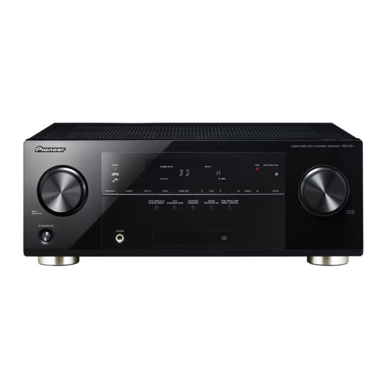
Pioneer VSX-821-K Service Manual
Audio/video multi-channel receiver
Hide thumbs
Also See for VSX-821-K:
- Operating instructions manual (144 pages) ,
- Specifications (2 pages) ,
- Quick start manual (156 pages)
Table of Contents
Advertisement
AUDIO/VIDEO MULTI-CHANNEL RECEIVER
VSX-821-K
VSX-921-K
VSX-521-K
THIS MANUAL IS APPLICABLE TO THE FOLLOWING MODEL(S) AND TYPE(S).
Model
Type
VSX-821-K
CUXCNSM
VSX-921-K
UXCNCB
VSX-521-K
CUXCNSM
For details, refer to "Important Check Points for good servicing".
PIONEER CORPORATION
PIONEER ELECTRONICS (USA) INC. P.O. Box 1760, Long Beach, CA 90801-1760, U.S.A.
PIONEER EUROPE NV Haven 1087, Keetberglaan 1, 9120 Melsele, Belgium
PIONEER ELECTRONICS ASIACENTRE PTE. LTD. 253 Alexandra Road, #04-01, Singapore 159936
PIONEER CORPORATION
Power Requirement
AC 120 V
AC 120 V
AC 120 V
1-1, Shin-ogura, Saiwai-ku, Kawasaki-shi, Kanagawa 212-0031, Japan
2011
VSX-821-K
K-IZV MAR.
ORDER NO.
RRV4167
Remarks
2011 Printed in Japan
Advertisement
Table of Contents
Troubleshooting

Related Manuals for Pioneer VSX-821-K


Summary of Contents for Pioneer VSX-821-K
- Page 1 PIONEER CORPORATION 1-1, Shin-ogura, Saiwai-ku, Kawasaki-shi, Kanagawa 212-0031, Japan PIONEER ELECTRONICS (USA) INC. P.O. Box 1760, Long Beach, CA 90801-1760, U.S.A. PIONEER EUROPE NV Haven 1087, Keetberglaan 1, 9120 Melsele, Belgium PIONEER ELECTRONICS ASIACENTRE PTE. LTD. 253 Alexandra Road, #04-01, Singapore 159936...
-
Page 2: Safety Information
PIONEER Service Manual. A subscription to, or additional copies of, Also test with plug reversed Earth PIONEER Service Manual may be obtained at a nominal (Using AC adapter ground charge from PIONEER. plug as required) - Page 3 To protect products from damages or failures during transit, the shipping mode should be set or the shipping screws should be installed before shipment. Please be sure to follow this method especially if it is specified in this manual. VSX-821-K...
-
Page 4: Table Of Contents
4.1 OVERALL WIRING DIAGRAM............................14 4.2 AUDIO BLOCK DIAGRAM (for VSX-821-K, VSX-521-K)....................16 4.3 AUDIO BLOCK DIAGRAM (for VSX-921-K)........................18 4.4 D-MAIN BLOCK DIAGRAM (for VSX-821-K, VSX-521-K) ....................20 4.5 D-MAIN BLOCK DIAGRAM (for VSX-921-K) ........................22 4.6 VIDEO BLOCK DIAGRAM ............................24 4.7 POWER SUPPLY and MAIN UCOM BLOCK DIAGRAM ....................26 5. -
Page 5: Service Precautions
GYP1008 0.3 in dia. 1.2 SERVICE NOTICE • Discharging For more detail, please refer to "7. DISASSEMBLY - 1. Discharging". • Notes on Ground Points Connection For more detail, please refer to "7. DISASSEMBLY - 2. Notes on Ground Points Connection". VSX-821-K... -
Page 6: Specifications
2. SPECIFICATIONS VSX-821-K Amplifier section Digital In/Out Section Continuous average power output of 80 watts* per HDMI terminal............Type A (19-pin) channel, min., at 8 ohms, from 20 Hz to 20 000 Hz with HDMI output type............5 V, 100 mA no more than 0.08 %** total harmonic distortion. - Page 7 Frequency Range (AM)........530 kHz to 1700 kHz Antenna (AM)...............Loop antenna Accessories AM loop antenna FM wire antenna (E601019000010-IL) (E605010140010-IL) Remote control Microphone (for Auto MCACC setup) iPod cable Dry cell batteries (APM7008) (L308102013020-IL) (8300762100010-IL) (AAA size IEC R03) x2 VSX-821-K...
- Page 8 Antenna Input (FM)..........75 Ω unbalanced Frequency Range (AM)........530 kHz to 1700 kHz Antenna (AM)...............Loop antenna Accessories AM loop antenna FM wire antenna (E601019000010-IL) (E605010140010-IL) Remote control Microphone (for Auto MCACC setup) Dry cell batteries (APM7008) (8300761900010-IL) (AAA size IEC R03) x2 VSX-821-K...
-
Page 9: Basic Items For Service
GGD1740 Lubricants and Glues List Name Part No. Remarks Silicon grease GEM1057 Refer to "9.2 EXTERIOR SECTION (VSX-821-K, VSX-921-K)" and "9.3 EXTERIOR SECTION (VSX-521-K)". Silicon adhesive GYA1011 Refer to "9.2 EXTERIOR SECTION (VSX-821-K, VSX-921-K)" (KE40RTV-W) and "9.3 EXTERIOR SECTION (VSX-521-K)". -
Page 10: Pcb Locations
3.3 PCB LOCATIONS VSX-821-K, VSX-921-K • This photo. is VSX-821-K. AUDIO ASSY BT ASSY VIDEO ASSY SUBWOOFER ASSY CPU ASSY MAIN ASSY D-MAIN ASSY STANDBY ASSY WIRE GUIDE B ASSY BRIDGE B ASSY BRIDGE A ASSY AMP ASSY GUIDE R ASSY... - Page 11 2..STANDBY ASSY (VSX-821-K) 7028070225030-IL 2..WIRE GUIDE A ASSY 7028070276070-IL 2..STANDBY ASSY (VSX-921-K) 7028070225070-IL 2..WIRE GUIDE B ASSY 7028070277070-IL 1..FRONT ASSY (VSX-821-K) 7025HK1011013-IL 1..AMP1 ASSY (VSX-821-K ONLY) 7025HK1011017-IL 1..FRONT ASSY (VSX-921-K) 7025HK1014013-IL 2..AMP ASSY (VSX-821-K ONLY) 7028070241030-IL 2..FRONT ASSY 7028070211050-IL 2..POWER ASSY 7028070212050-IL 1..AMP2 ASSY (VSX-921-K ONLY)
- Page 12 2..POWER ASSY 7028070212050-IL 1..AMP1 ASSY 7025HK1011017-IL 2..MIC ASSY 7028070213020-IL 2..AMP ASSY 7028070241030-IL 2..HEADPHONE ASSY 7028070215050-IL 1..BT ASSY 7025HK1009019-IL 1..AUDIO ASSY 7025HK1011014-IL 2..BT ASSY 7028070231010-IL 2..AUDIO ASSY 7028070181030-IL 1..VIDEO ASSY 7025HK1011016-IL 1..D-MAIN ASSY 7025HK1012012-IL 2..VIDEO ASSY 7028070261060-IL 2..D-MAIN ASSY 7028070191020-IL VSX-821-K...
- Page 13 VSX-821-K...
-
Page 14: Block Diagram
2.FR 1.SBL 8.HIGHGND 2.NC 9.HIGHGND 4.SL 3.SBR 10.PREGND 5.SR 1 2 3 9 10 MAIN ASSY (MAIN) (MAIN) (MAIN) MAIN TRANS (VSX-821-K: 70280702710H0-IL) (VSX-921-K: 70280702710G0-IL) (VSX-521-K: 70280702710D0-IL) 1.FLAC 2.FLCT 1.FLAC 3.FLAC 2.FLCT 3.FLAC 4.GNDU 5.CPU_+3.3V 6.CPU_ST_VCC 7.PDN CP701 8.STBY_RLY 9.HDMI+12V... - Page 15 VIDEO ASSY (VSX-821-K/521:7028070261060-IL) (VSX-921-K:7028070261070-IL) 1.+5V 2.GNDV 3.Y_IN 4.GNDV 27.SW_MUTE 1.F_VIDEO 1.F_VIDEO 5.CB_IN 26.SW_OUT 2.GNDD 2.GNDD 6.GNDV 25.AGND 3.NJW1327_SDA 3.NJW1327_SDA 7.CR_IN 24.TUNER_R 4.NJW1327_SCL 4.NJW1327_SCL 8.GNDV 23.AGND 5.OSD_RST 1.SW_MUTE 5.OSD_RST 9.CVBS_IN 22.TUNER_L 6.OSD_CE 2.SW_OUT 10.CVBS_DET 21.AGND 6.OSD_CE 1/4- 4/4) 3.GNDA 7.OSD_DATA 7.OSD_DATA 11.COMP_DET...
-
Page 16: Audio Block Diagram (For Vsx-821-K, Vsx-521-K)
4.2 AUDIO BLOCK DIAGRAM (for VSX-821-K, VSX-521-K) FRONT ASSY USB ASSY (VSX-821-K only) AUDIO ASSY MAIN ASSY BT ASSY MIC ASSY F-VIDEO ASSY HEADPHONE ASSY (VSX-821-K only) VSX-821-K... - Page 17 MAIN ASSY AMP ASSY SUBWOOFER MAIN ASSY ASSY VSX-821-K...
-
Page 18: Audio Block Diagram (For Vsx-921-K)
4.3 AUDIO BLOCK DIAGRAM (for VSX-921-K) USB ASSY FRONT ASSY AUDIO ASSY used MAIN AS used BT ASSY MIC ASSY F-VIDEO ASSY HEADPHONE ASSY VSX-821-K... - Page 19 MAIN ASSY AMP ASSY SUBWOOFER ASSY MAIN ASSY VSX-821-K...
-
Page 20: D-Main Block Diagram (For Vsx-821-K, Vsx-521-K)
4.4 D-MAIN BLOCK DIAGRAM (for VSX-821-K, VSX-521-K) D-MAIN ASSY VSX-821 only VSX-821-K... - Page 21 VSX-821-K...
-
Page 22: D-Main Block Diagram (For Vsx-921-K)
4.5 D-MAIN BLOCK DIAGRAM (for VSX-921-K) D-MAIN ASSY VSX-821-K... - Page 23 VSX-821-K...
-
Page 24: Video Block Diagram
4.6 VIDEO BLOCK DIAGRAM VIDEO ASSY VSX-921 only COMPONENT & CVBS SELECT NJW1327 TV/SAT DET. VIDEO FRONT-V VSX-921, VSX-821 only 1V(0dB) COMP1-Y COMP2-Y UP-Y COMP1-Cb COMP2-Cb UP-Cb COMP1-Cr COMP2-Cr UP-Cr 1V(0dB) 1V(0dB) 1V(0dB) DET. 1V(0dB) VSX-821-K... - Page 25 921 only DET. DET. VSX-821-K...
-
Page 26: Power Supply And Main Ucom Block Diagram
4.7 POWER SUPPLY and MAIN UCOM BLOCK DIAGRAM MAIN ASSY S1(AMP B+/B-) Not use S2(+12V,-12V) MAIN TRANS S3(DSP, HDMI) S4(USB) VSX-921/821 only AC CORD S4(FLT) SUB TRANS STANDBY ASSY VSX-821-K... - Page 27 Not used CPU ASSY only VSX-821-K...
-
Page 28: Diagnosis
Check the IC1324 DSP power pin (cvdd and dvdd) and Is the voltage of 1.2 V output? its peripheral circuits or must be replaced IC1324, REG1302. Check the IC1324 DSP power pin (cvdd and dvdd): cvdd: 1.2 V, dvdd: 3.3 V. DSP +3.3V line is OK. VSX-821-K... - Page 29 Is the voltage 5 V output? Is pin 6 (en) of IC1325 high? the SUB CPU (IC1316). Check the IC1318 power pin (dvdd, avdd, PVDD) : dvdd: 5 V, avdd: 5 V, PVDD: 5 V HDMI+5V line is OK VSX-821-K...
- Page 30 USB (iPod). IC1318 (pin 71) from USB Assy Can observe the Check the path to CP1303 connector. Check the USB Assy. digital signal? (0 V ↔ 3.3 V) Check that the data and clock signals are output. VSX-821-K...
- Page 31 Is there a bit clock output? (0 V ↔ 3.3 V) Check the path between IC1322 pin 1 Is the voltage of IC1322 To Step 7 and CPU Assy. pin 1 0 V? *IC1322 pin 1 0 V: DIR Replace IC1322. 3.3 V: HDMI VSX-821-K...
- Page 32 (0 V ↔ 3.3 V) IC1318 (pin 25) surround back L/R data Is there a data input? (0 V ↔ 3.3 V) To Step 8 Check the path between IC1324 and data & address lines. SDRAM (IC1321), FLASH ROM (IC1323). VSX-821-K...
- Page 33 Is there a audio signal Is the output 2.5 V fixing? output? IC1318 (pin 39) IC1318 (pin 39) LFE out LFE out Is there a audio signal Is the output 2.5 V fixing? output? Replace IC1318. VSX-821-K...
- Page 34 Turn on the power of the receiver and equipments which was connected with HDMI. Function switch (VIDEO or BD or DVD or DVR/BDP) Switch the function that HDMI was assigned. Factory shipments setting: HDMI1: DVR/BDR HDMI2: DVD HDMI3: BD HDMI4: VIDEO1 To Step 2 VSX-821-K...
- Page 35 Is the voltage 3.3 V? Replace Q1318. is 0 V? (base is 3.3 V) is 2.6 V? Check the parts and pattern Check the parts and pattern in the path. in the path of Q1318, Q1319 Replace Q1318,Q1319. etc. VSX-821-K...
- Page 36 Is the voltage 0 to 3.3 V? (0 to 3.3 V) CP1306 (pin 12) CP1306 (pin 8) MAIN_IRQ SCDO_MAIN Is there a data input? Is there a data input? Diagonose the MAIN Assy. Diagonose the MAIN Assy. (0 to 3.3 V) (0 to 3.3 V) VSX-821-K...
- Page 37 59 of IC1316. IC1302 (pin 21) To Step 4 Is there a 28.63636 MHz Replace IC1302 or X1301. output? IC1302 (pin 22) Check the path to pin 22 of Is there a 28.63636 MHz IC1302. Replace IC1302. output? To Step 5 VSX-821-K...
- Page 38 Is there a same signal JACK1303. If IC1308 or as IC1308 pin 48 when JACK1303 is failure, selecting IN1? replace IC1308 or JACK1303. (0 to 5 V) JACK1302 (pin 18)//+5V_R2//IN2 (BD) JACK1301 (pin 18)//+5V_R1//IN3 (DVD) JACK1300 (pin 18)//+5V_R0//IN4 (DVR/BDR) VSX-821-K...
- Page 39 IC1302. (0 to 3.3 V)? IC1308 (pins 30,31,33,34,36,37,39,40) TMDS OUTPUT To Step 8 Check the IC1308 or IC1303. Are there signals If IC1308 or IC1303 is failure, (approx. 0.5 Vp-p) replace IC1308 or IC1303. IN all lines? VSX-821-K...
- Page 40 Check the pattern in the path. Is the voltage of 5V input? (to chassis) REG2 (pin 2) 3.3 V output Replace REG2. Is the voltage 3.3 V output? Is REG2 abnomally hot? The output and GND may be short-circuited. Check the path between them. VSX-821-K...
- Page 41 SDRAM (IC803), several seconds later,does SDCLK Operation of IC801 is OK. FLASH ROM (IC802), and IC801 change 12 MHz to 80 MHz? Go to step 3. are may not be connected. Operation of IC801 is OK. Go to step 3. VSX-821-K...
- Page 42 Go to step 4. Step 4: Audio out check CN802 (pin 1) S/PDIF output Check the path between Is there a S/PDIF signal? Replace IC801. IC801 (pin 105). Check the parts and pattern CN802 and IC801. Refer to "[1] DSP TROUBLESHOOTING." VSX-821-K...
- Page 43 MAIN and CPU Assys. Step 3: BT_ID CP603 (pin 7) Check the pattern in the path and Is the voltage 0.7 to 1.2 V? SUBWOOFER Assy. Check the pattern in the path and To Step 4 MAIN and CPU Assys. VSX-821-K...
-
Page 44: Adapter Error Message
• Confirm a detection port at intervals of 20 msec to 50 msec (*2), and judge it as an overcurrent when you detected an error consecutively three times. *2 It is assumed that it is fixed value of the 20 msec to 50 msec degree. VSX-821-K... -
Page 45: Usb / Ipod Error Message
E R R 1 iPod/USB communication error Generation error I / U E R R 2 Loading error I / U E R R 3 OverHeat error I / U E R R 4 No Track Caution T R A C K VSX-821-K... -
Page 46: Detection Circuit
5.4 DETECTION CIRCUIT [1] Overload and DC Protection Circuit VSX-821-K... - Page 47 [2] TEMP Protection Circuit VSX-821-K...
-
Page 48: Service Mode
DC error." If a protection function is activated immediately after the previous protection function is canceled, cancel that protection function again then enter STBY mode immediately. You can then see the error logs, following the above procedures, until a next protection function is activated. VSX-821-K... - Page 49 1. When the procedures for Reset mode for numbers of protection detections are completed, all the counters will be reset to "000." 2. Prohibitions: The protection detection counts cannot be cleared (reset to 000) with the MEMORY CLEAR process. They can only be cleared when the procedures of Reset mode are completed. VSX-821-K...
- Page 50 Description of Indications usually (Normal display) Normal display (DC detection) (Auto) (RECEIVER POWER OFF) *1, *2 3.2 OVERLOAD (overcurrent) error detection Key Operation FL Display Time (sec.) Description of Indications usually Normal display (Normal display) (OVERLOAD detection) (Auto) (RECEIVER POWER OFF) VSX-821-K...
- Page 51 Normal display (Normal display) [Detailed explanations] Simultaneously holding the [ADVANCD SURROUND] and [STANDBY/ON] keys on the front panel pressed for 2 seconds will cancel Key Input Inhibition mode after a DC error detection and turn the unit ON. VSX-821-K...
-
Page 52: Disassembly
(3) Check that the voltage between the –30V terminal is less than 1 V, using a tester. ∗ Be sure to connect the GND terminal of the tester to the chassis. ∗ If the voltage is still 1 V or higher, repeat Step (2). CN704A FRONT Assy 47 - 100 ohms (2 W or higher) VSX-821-K... - Page 53 Without grounding connection, the protection circuit will be activated. After repairing, be sure to remove the ground wire before reassembling. Speaker chassis Chassis back GND wire (Be sure to disconnect the GND wire before reassembly.) Main capacitor GND MAIN Assy (SIDE B) VSX-821-K...
- Page 54 3. Disassembly Note: The photo. without the explanatory note is VSX-821-K. [1] Front Panel Section Remove the cabinet by removing the 10 screws. (1) Remove the five screws. (BBZ30P080FTB) • Bottom view (VSX-821-K, VSX-921-K) (2) Remove the two screws. (1500001206010-IL) (3) Remove the one screw.
- Page 55 (1) Remove the three screws. (BBZ30P080FTC) • Bottom view (2) Remove the six screws. (BBZ30P080FTC) GUDE R Assy GUDE L Assy WIRE GUIDE A Assy (3) Remove the one screw. (BBZ30P080FTC) (4) Remove the WIRE GUIDE A Assy. (5) Cut the binder. VSX-821-K...
- Page 56 (6) Disconnect the one connector. (CP401) CP401 AMP Assy (7) Connect the extension jig cable. Extension jig cable (8) Rotate the heatsink section in the direction of (VSX-821-K, VSX-521-K: GGD1739) the arrow. (VSX-921-K: GGD1740) AMP Assy CP401 Heatsink VSX-821-K...
- Page 57 [3] D-MAIN Assy Remove the cabinet by removing the 10 screws. (1) Remove the five screws. (BBT30P100FTB) (VSX-821-K, VSX-921-K) Chassis back (2) Remove the five screws. (BSZ30P040FTB) ×3 ×5 • Rear view (VSX-521-K) Chassis back ×3 ×5 • Rear view BRIDGE A Assy (3) Cut the binder.
- Page 58 [4] MAIN Assy Remove the cabinet by removing the 10 screws. [4-1] Chassis back, D-MAIN Assy (VSX-821-K, VSX-921-K) Chassis back ×3 (1) Remove the 14 screws. (BBT30P100FTB) ×5 (2) Remove the five screws. (BSZ30P040FTB) (3) Remove the D-MAIN Assy. (See procedure [3].) •...
- Page 59 (2) Tighten then loosen the screw in each of the MAIN Assy Screwdriver four holes for temporary joining that are located on the rear side of the main chassis. (This is for shaving the thread grooves to facilitate attachment in the next step.) Main chassis Support VSX-821-K...
- Page 60 (1) Remove the one screw and remove the earth WIRE GUIDE A Assy WIRE GUIDE A Assy lead jumper. (BBZ30P080FTC) (2) Reassemble the earth lead jumper. (3) Remove the WIRE GUIDE A Assy. Earth lead jumper Earth lead jumper VSX-821-K...
- Page 61 Insulation sheet (5) Reassemble the D-MAIN Assy with extension jig cables. (See procedure [3].) (6) Insert any insulation sheet between D-MAIN Assy and MAIN Assy. (7) Connect the extension jig FFC. D-MAIN Assy CN704B Extension jig FFC CPU Assy (GGD1738) VSX-821-K...
-
Page 62: Each Setting And Adjustment
When any of the following assemblies is replaced AMP Assy "8.3 IDLE CURRENT ADJUSTMENT" (All channel) Other assemblies No adjustment required When any of the following parts is replaced AMP Assy "8.3 IDLE CURRENT ADJUSTMENT" (Only channel of replacement parts) Other assemblies No adjustment required VSX-821-K... -
Page 63: Updating Of The Firmware
Insert the FFC with its contact surface facing the " mark. (SUB microcomputer) RS-232C Straight cable 10P to 10P FFC UPDATE jig GGF1642 (MAIN microcomputer) Rear side (VSX-821-K) Straight Cable Adapter JIG's side (1) MAIN and SUB microcomputers update [Procedures] for MAIN microcomputer 1. Unplug the AC cord. - Page 64 [ if the following messages are displayed ] 2 Update the MCU Press the E.P.R … button Please push the cancel button and press the JIG's Press OK button. RESET button. And confirm a connection of FFC. Please return to procedure 7. VSX-821-K...
- Page 65 Set Baud rate to 38400. (Default Baud rate is 9600) Press the OK button. 2 Update the MCU. E.P.R=>Erase+Program+Read 2 Update the MCU 11. Turn the main unit off. (STANDBY mode) Press the E.P.R … button Disconnect the FFC cable. Press OK button. VSX-821-K...
- Page 66 USB/iPod FUNCTION is selected. (Except for VSX-521 & 421) 13. Turn the main unit off. (2) How to Update the USB Microcomputer (VSX-821-K, VSX-921-K ONLY) [Procedures] 1. Copy the "VSX_USB.rom" file to the root directory of a USB memory device.
- Page 67 8.3 IDLE CURRENT ADJUSTMENT for VSX-821-K, VSX-521-K When any component parts which are within the red square on the following circuit diagram are replaced, the idle current adjustment of that channel is required. (Idle current adjustment for another channel is not required.) However, when any capacitors are replaced, the adjustment is not required.
- Page 68 TP406 pin 3 (–) TP407 pin 1 (+) VR407 TP407 pin 3 (–) • Adjustment points and measurement points..see fig.2. SIDE A AMP ASSY SL_VR401 FL_VR404 C_VR403 SR_VR405 FR_VR402 SBL_VR406 SBR_VR407 SL_TP401 FL_TP404 C_TP403 SR_TP405 FR_TP402 SBL_TP406 SBR_TP407 Fig.2 VSX-821-K...
- Page 69 VSX-821-K...
-
Page 70: Exploded Views And Parts List
For the applying amount of lubricants or glue, follow the instructions in this manual. (In the case of no amount instructions, apply as you think it appropriate.) 9.1 PACKING SECTION Poly bag packing style Tape (clear) Cord AC VSX-821-K, VSX-921-K only Sheet SP caution Dry cell batteries Label serial Label getter... - Page 71 (En, Frca, Es) 7 Box, Gift See Contrast table (2) 8 Cushion, Snow 6230212914000-IL 9 PE, Sheet 6327040059000-IL (2) CONTRAST TABLE VSX-821-K/CUXCNSM, VSX-921-K/UXCNCB and VSX-521-K/CUXCNSM are constructed the same except for the following: VSX-821-K VSX-921-K VSX-521-K Mark Symbol and Description /CUXCNSM /UXCNCB...
- Page 72 9.2 EXTERIOR SECTION (for VSX-821-K, VSX-921-K) Cushion EVA Cushion EVA Cushion EVA VSX-821-K...
- Page 73 ×38 TUNER FM/AM Main chassis Silicon adhesive (GYA1011) Cushion EVA Silicon grease Heatsink (GEM1057) Cushion EVA VSX-821-K...
-
Page 74: Audio Assy
(1) EXTERIOR SECTION (for VSX-821-K, VSX-921-K) PARTS LIST Mark No. Description Part No. Mark No. Description Part No. 46 Plate 4470212096000-IL 1 MAIN Assy See Contrast table (2) 47 Plate 4470212066000-IL 2 SUBWOOFER Assy 7028070272070-IL 48 Sheet 1217211472000-IL 3 GUIDE L Assy... - Page 75 (2) CONTRAST TABLE VSX-821-K/CUXCNSM and VSX-921-K/UXCNCB are constructed the same except for the following: VSX-821-K VSX-921-K Mark Symbol and Description /CUXCNSM /UXCNCB MAIN ASSY 70280702710H0-IL 70280702710G0-IL AMP ASSY 7028070241030-IL 7028070251040-IL VIDEO ASSY 7028070261060-IL 7028070261070-IL CPU ASSY 7028070221030-IL 7028070221070-IL STANDBY ASSY...
- Page 76 9.3 EXTERIOR SECTION (for VSX-521-K) Cushion EVA Cushion EVA VSX-821-K...
Need help?
Do you have a question about the VSX-821-K and is the answer not in the manual?
Questions and answers
No power tried turn it on
Your Pioneer VSX-821-K is not turning on because power is reaching the unit but not passing through the transformer on the power supply board. The relay is not clicking, which means it is not receiving the signal to turn on. This suggests a potential issue with the power supply board or its control circuitry.
This answer is automatically generated