
Related Manuals for Fender Twin Amp 1994


Summary of Contents for Fender Twin Amp 1994
-
Page 1: Service Manual
’94 TWIN AMP p/n 02-4809-000(120V) SERVICE MANUAL CONTENTS: Notices Specifications Parts lists: PCB assembly Chassis assembly Cabinet assembly End item Schematics/diagrams Fender Musical Instruments Corp. 7975 North Hayden Road Scottsdale, AZ 85258... -
Page 2: Important Notice
Fender Musical Instruments Co. All specifications subject to change without notice. For warranty repair service, only Fender specified part numbers are to be used. It is recommended they also be used for post-warranty maintenance and repair. -
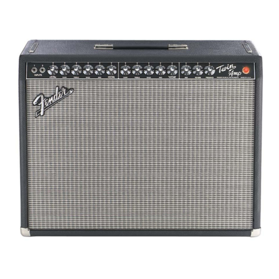
Page 3: Specifications
Amplifier Load Impedance: Power Output: OUTPUT HIGH setting: 100 watts RMS, 5% THD. OUTPUT LOW setting: 25 watts RMS, 5% THD. Speaker Complement: Two Fender P.N 026488 Special Design 12” 8 ohm speakers wired in series. Dimensions: Height: 20 3/4” (52.7 cm) Width: 26 3/8”... -
Page 4: Theory Of Operation
Channel Two is like owning a second, modern hot-rodded amp with more soaring gain than previously found in a Fender tube amp. The signal from pin 9 of Relay K1B feeds through the Channel Two Gain control (R25) to the first (V3A) and then second (V3B) stage of the overdrive circuitry. - Page 5 ’94 TWIN AMP THEORY OF OPERATION(CONT) Reverb return circuit uses JFET Q1. Without a footswitch connected to the footswitch jack, diode CR17 enables the reverb to function. V6A amplifies the reverb return signal. Note that V6A should provide a minimum gain of 49. The output from V6A drives the Reverb control (R62), then sums with the dry signal through R63.
-
Page 6: Parts List
’94 TWIN AMP THEORY OF OPERATION(CONT) switch from +454Vdc to +230Vdc. This voltage change only affects the four output tubes. The high voltage supplies for the preamp tubes are tapped off prior to the output switch (S9). When switching the high voltages at the power tubes, the negative Bias voltage must also be switched. -
Page 7: Chassis Assembly
’94 TWIN AMP PRINTED CIRCUIT BOARD ASSEMBLY (CONT) PART # DESCRIPTION REFERENCE DESIGNATION 041511 CONTROL SNAPIN 250K B DUAL (MIX) 041512 CONTROL SNAPIN 1M 30A R11 (CHANNEL 1 CLEAN VOLUME) 037596 CONTROL SNAPIN 1 MEG J TAPER R8,25 (CHANNELS 1,2 GAIN) 026133 CONTROL TRIM 25K LIN R92,94... - Page 8 ’94 TWIN AMP CHASSIS ASSEMBLY (CONT) PART # DESCRIPTION REFERENCE DESIGNATION 023580 TUBE SOCKET 8 PIN XV9,10,11,12 023606 TUBE SOCKET 9 PIN XV1,2,3,4,5,6,7,8 039214 TUBE VACUUM 5881/6L6WGC V9,10,11,12 9904300100 WASHER LCK INTL 3/5X.681X.032 (@J14,16) 026564 WSHR FLAT .284X1/2ZI (@R92,94 BIAS/BALANCE POTS) 027520 WSHR FLAT .380X.630 FIBER (@J14,15,16)
- Page 9 ’94 TWIN AMP BLOCK DIAGRAM...
- Page 10 This addendum contains important modification and revision information including parts and revision “C” schematics. Please attach to the existing service manual for the ’94 Twin Amp. CONTENTS: Notices Description of changes Parts list Schematics/diagrams Fender Musical Instruments Corp. 7975 North Hayden Road Scottsdale, AZ 85258...
- Page 11 Fender Musical Instruments Co. All specifications subject to change without notice. For warranty repair service, only Fender specified part numbers are to be used. It is recommended they also be used for post-warranty maintenance and repair.
- Page 12 ’94 TWIN AMP ADDENDUM DESCRIPTION OF CHANGES All of the following modifications are present on revision “E” printed circuit boards. Some of the other modifications appear on earlier revision PCBs. The PCB revision level is located on the solder side of the centermost PCB, near the orange wire and filter capacitor C40.
- Page 13 ’94 TWIN AMP ADDENDUM PARTS LIST REVISIONS PRINTED CIRCUIT BOARD ASSEMBLY QTY PART # DESCRIPTION REFERENCE DESIGNATION 024819 CAP AE AX 22uF 500V C22,42,43,44,51 024820 CAP AE AX 47uF 350V C40,41 025995 CAP CD 8200PF 1000V 20% 026730 DIODE 1N4006 800V CR2,3,5-11,14,15,34-37 006260 DIODE 1N4448 SIGNAL...
- Page 16 TECH NOTES Fender Musical Instruments Corp. 7975 North Hayden Road Scottsdale, Arizona 85258 TECH NOTE # TN96 - 3 ISSUE DATE: March, 1996 ISSUED BY: C. Colaço PAGE: 1 of 2 PRODUCT(S) AFFECTED: '94 TWIN AMP (All Serial numbers prior to LO-673648 should require this modification) SYMPTOMS: Overheating of power tubes when in the LOW OUTPUT power mode.
- Page 17 TECH NOTE # TN96 - 3 PAGE: 2 of 2 To gain access to the solder side of the PCB, disconnect the Black wires from CP1 & CP2. Disconnect the wires at the Stand-by switch. This will allow the PCB to be tilted up from the rear.