Table of Contents
Advertisement
Quick Links
Download this manual
See also:
User Manual
Advertisement
Table of Contents

Related Manuals for Asus M530w


Summary of Contents for Asus M530w
- Page 1 華 碩 電 腦 華 碩 電 腦 TSD ■ Lv3Lv4 Repair Manual ASUS M530w Level 3 & Level 4 Service Manual ASUS Proprietary...
-
Page 2: Table Of Contents
5.2 Measure method ..................15 5.3 Repair method ..................15 6. USB/CHARGING................16 6.1 Introduction ..................... 16 6.2 Repair method ..................16 7. KEYPAD................... 17 7.1 Introduction ..................... 17 7.2 Measure method ..................20 7.3 Repair method ..................20 ASUS Proprietary... - Page 3 Introduction ....................32 11.1 2M camera..................... 32 11.1.1 Measure method ................32 11.1.2 Repair method ................. 33 11.2 VGA camera..................... 33 11.2.1 Measure method ................. 34 11.2.2 Repair method ..................34 12. SIM INTERFACE................35 12.1 Introduction ..................... 35 ASUS Proprietary...
- Page 4 15.4 Test Environments Setup................ 41 15.4.1 Instrument linking ................41 15.4.2 Fixture....................42 16. RF BLOCK DIAGRAM ..............43 16.1 GSM block diagram ................43 16.2 WCDMA block diagram..............44 17. RF TX/RX PATH AND TEST POINTS ........... 45 ASUS Proprietary...
- Page 5 19.1 General GSM Tx debug ............... 61 19.2 General GSM Rx debug............... 70 19.3 General WCDMA Tx debug..............77 19.4 General WCDMA Rx debug ............... 84 20. APPENDIX................... 88 20.1 GSM/WCDMA wireless test..............88 20.2 Bluetooth test ..................90 20.3 WiFi test....................92 ASUS Proprietary...
-
Page 6: Appearance
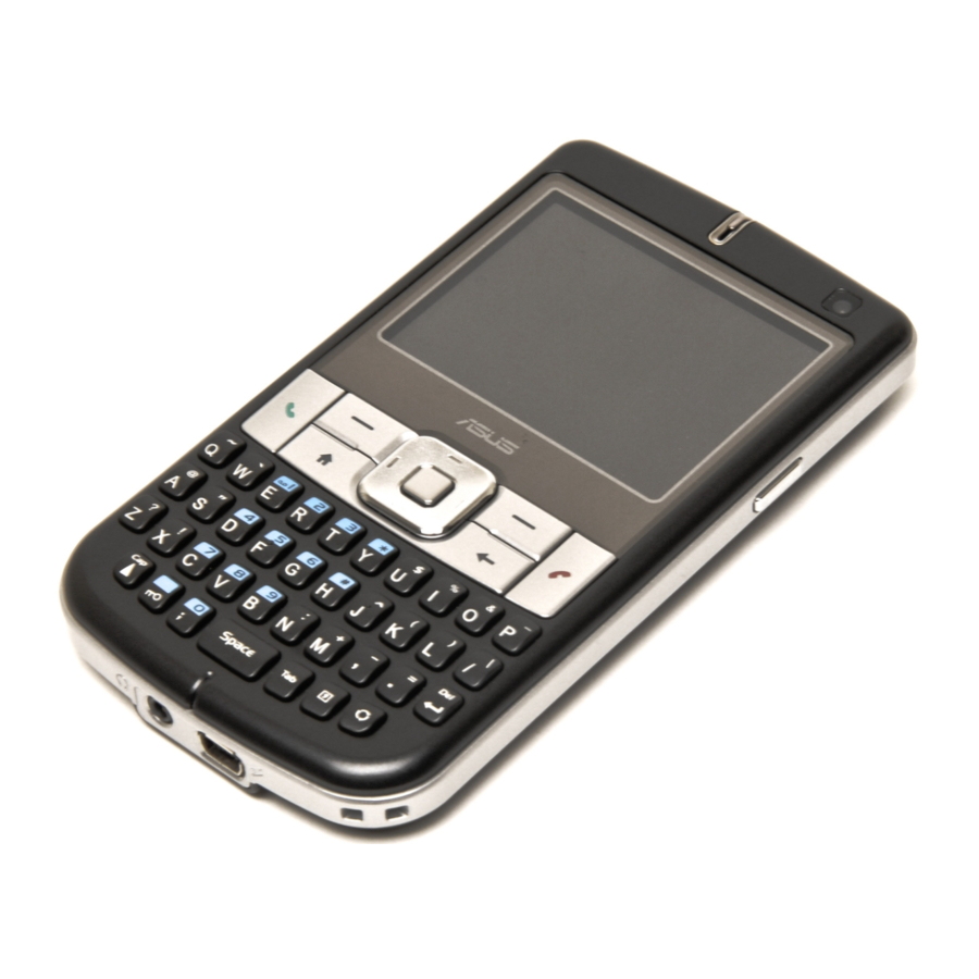
華 碩 電 腦 華 碩 電 腦 TSD ■ Lv3Lv4 Repair Manual 1. APPEARANCE 1.1 BOX APPEARANCE ASUS Proprietary... -
Page 7: Main Component Name & Location
華 碩 電 腦 華 碩 電 腦 TSD ■ Lv3Lv4 Repair Manual 1.2 MAIN COMPONENT NAME & LOCATION Main Board TOP LAYER (1) Application CPU ( Bulverde PXA270)-U1 ASUS Proprietary... - Page 8 華 碩 電 腦 華 碩 電 腦 TSD ■ Lv3Lv4 Repair Manual (2)Communication CPU ( Hermon PXA900 )-U17 (3) PSRAM (MT45W1MW16PDGA-70WT)-U18 (4)Cedar Creak-U19 (5) (6)SDRAM-U2、U3 (7)NAND FLASH( M-Systems H3)-U4 (8)PMIC( DA9030 )-U20 ASUS Proprietary...
- Page 9 華 碩 電 腦 華 碩 電 腦 TSD ■ Lv3Lv4 Repair Manual Main Board BOTTOM LAYER TP83 TP82 TP36 TP88 TP87 TP84 TP86 TP85 TP40 TP90 TP50 TP75 TP74 TP92 TP33 TP47 TP91 TP46 TP89 TP35 TP34 ASUS Proprietary...
-
Page 10: Block Diagram
Landscape (Discrete TPBGA) PWR I2C Cedar Creek Codec+AFE RF Circuit Qwerty (CSR BC-04) Keypad Hermon Power PMIC Bulverde power Audio (Arava) speaker MIC + Speaker + Receiver Charger Battery Headset Amp. USB SW. VCHG USB + Headset Jack ASUS Proprietary... -
Page 11: Hardware Equipment
Check the signals waveforms and voltage levels. 3.3 USB Download Cable The software bin file can be downloaded into the handset by the M530w USB download cable. The PC also can connect to the handset by it. USB Download Cable 3.4 Earpiece... -
Page 12: Download Procedure
1. Set up the power supply voltage and current at 4V and 1A. Connect to the battery connector positive and negative of the handset. 2. Press the POWER ON Key and Down button. The handset would power up and enter the download mode. Power on key Down button ASUS Proprietary... -
Page 13: Repair Method
腦 TSD ■ Lv3Lv4 Repair Manual 3. The handset is connected the PC by the USB Download Cable. 4. Execute the ASUS 3G Download Tool.exe program, and press “Browse” to select image. 5. Press Start button to burn image。 4.3 Repair method 1. -
Page 14: Lcm Display
碩 電 腦 TSD ■ Lv3Lv4 Repair Manual 5. LCM DISPLAY 5.1 Introduction The M530w LCM pixel resolution is 320 * 240. The backlight is white LED, and the driver IC is MAX8595ZETA (U12). Backlight Driver D206 L201 BL_VBAT_IN BL_LX... -
Page 15: Measure Method
4. When the backlight is no function, please check if the MAX8595ZETA (U12)、C208、C210、C211、C212、L201、 D206、R214、R215、R223 and R224 are placed inversely, soldered poorly or short. 5. If the above cases are not found, try to change a new LCM. ASUS Proprietary... -
Page 16: Usb/Charging
電 腦 TSD ■ Lv3Lv4 Repair Manual 6. USB/CHARGING 6.1 Introduction The M530w power is supplied by the Lithium Ion battery. Therefore, it has the charging function. The M530w can be charged from the USB. Connector CON_VCHG_VBUS OVP_VCHG_VBUS [10] OVP_VCHG_VBUS 1.5A/32V... -
Page 17: Keypad
華 碩 電 腦 華 碩 電 腦 TSD ■ Lv3Lv4 Repair Manual 7. KEYPAD 7.1 Introduction The M530W has 54 keys,some of them are function key. KP_MKIN7 KP_MKIN6 KP_MKIN5 KP_MKIN4 KP_MKIN3 KP_MKIN2 KP_MKIN1 KP_MKIN0 KEY 36 KEY 37 KEY 45... - Page 18 0Ohm 0Ohm C657 C656 TACT_SWITCH_4P $0.01UF/50V TACT_SWITCH_4P 0.01UF/50V Power_ON Volume Up /OFF R665 KP_MKOUT2_SK KP_MKOUT2 0Ohm C659 $0.01UF/50V TACT_SWITCH_4P TACT_SWITCH_4P Camera Volume Down R668 R666 KP_MKOUT5_SK KP_MKOUT3_SK KP_MKOUT5 KP_MKOUT3 0Ohm 0Ohm C660 C658 $0.01UF/50V $0.01UF/50V Function Key Circuit ASUS Proprietary...
- Page 19 R658 0Ohm Keypad Connector Circuit KP_MKOUT6_JOG KP_MKOUT6 R663 0Ohm KP_MKIN0_JOG KP_MKIN0 R659 0Ohm KP_MKOUT2_JOG KP_MKOUT2 R660 0Ohm KP_MKOUT3JOG KP_MKOUT3 R661 0Ohm PUSH C652 C653 C654 C655 GND1 GND2 GND3 GND4 P_GND1 P_GND2 NP_NC1 NP_NC2 SW_6P_8HOLD JOG DIAL Circuit ASUS Proprietary...
-
Page 20: Measure Method
5. Press Soft1 key will leave “Keypad/Button test”, therefore Soft1 key need press last. 7.3 Repair method 1. When the Keypad are no function, check if a. Keypad connector (CON9) are soldered poorly, open or short. b. Serial Resistors ( R651~R658 ) are soldered poorly, open or ASUS Proprietary... - Page 21 2. When the function key and JOG DIAL are no function, check if the sw1、sw2、sw3、sw4、sw5 and Keypad connector(CON9) are soldered poorly, damage or short. 3. If the above cases are not found, try to change the Keypad or Function Key (SW1~SW5). ASUS Proprietary...
-
Page 22: Keypad Led
1. Set up the power supply voltage and current at 4V and 1A. Connect to the battery connector positive and negative of the handset. 2. Press the POWER ON Key to power on the handset. 3. After entering the MMI Test Mode, select the “Led test” item. ASUS Proprietary... -
Page 23: Measure Method
KEYPAD connector (CON1 and CON2)、R25 are soldered poorly, damage, open or short. 2. When the Keypad not all LEDs can not turn on, change the new Keypad. If the above cases are not found, change the new Keypad. ASUS Proprietary... -
Page 24: Vibrator
3. After entering the MMI Test Mode, select the “set Vibrator“ test item. Press ”on”,the vibrator should vibrate. VBAT VIB_IN R216 0Ohm C213 0.1UF/10V D207 $VIBRATOR_2P 1SS400 VIB_D_AN VIB_OUT R218 0Ohm R220 5.1Ohm SI1012R VIBRATOR_EN [10] umt3_rohm ==> R222 sot_416 100KOhm Vibrator circuit ASUS Proprietary... -
Page 25: Repair Method
華 碩 電 腦 TSD ■ Lv3Lv4 Repair Manual 9.3 Repair method 1. Check if the R216、R218、R220、R222、D207、Q3、C213are placed inversely, soldered poorly, damage, open or short. 2. If the voltage of each pin is normal, change a new vibrator. ASUS Proprietary... -
Page 26: Acoustics
10. ACOUSTICS 10.1 HANDSET 10.1.1 Introduction The purpose of this test is mainly verifying the handset microphone、 speaker and receiver function. M530w has three kinds of the audio output and input Type Comment Handset Utilize the handset microphone and receiver. - Page 27 C339 C338 C332 C333 D307 D308 $33PF/50V $33PF/50V $33PF/50V $33PF/50V 331K 331K Receiver circuit L308 330Ohm/100Mhz C326 27PF/50V SP_OUT1 [10] Speaker_IN_P CON4 C327 Speaker_IN_N 27PF/50V POGO_2PIN D309 Speaker_CONNECTOR SP_OUT2 [10] PACDN045Y B6 C331 27PF/50V L309 330Ohm/100Mhz Speaker circuit ASUS Proprietary...
-
Page 28: Measure Method
1. When the microphone can’t work a. check if the microphone circuit are soldered poorly, damage or short. b. Check rubber set properly. c. If the above cases are not found, change the new microphone. 2. When the speaker can’t work ASUS Proprietary... - Page 29 Check the contact between the receiver pins and the pads on the main PCB (Is the pin oblique/sunk?) c. If the above cases are not found, change the new receiver. ASUS Proprietary...
-
Page 30: Earpiece
L304 1400Ohm/1Ghz HS_DETECT AJACK_EAR_L_SW AJACK_EAR_L R328 0Ohm AJACK_GND L305 1400Ohm/1Ghz NP_NC1 D302 D305 NP_NC2 R315 R316 R327 0Ohm MINI_JACK_6P C336 C337 C317 C318 30KOhm 30KOhm $331K $331K GND GND GND GND $33PF/50V $33PF/50V $100PF/50V $100PF/50V VSS_AUD Earpiece circuit ASUS Proprietary... -
Page 31: Repair Method
電 腦 TSD ■ Lv3Lv4 Repair Manual 10.2.3 Repair method 1. Check if the J1、L304、L305、R314、R315 and U14 are placed inversely, soldered poorly, damage or short. 2. If the above cases are not found, change the new Phone Jack. ASUS Proprietary... -
Page 32: Camera
華 碩 電 腦 華 碩 電 腦 TSD ■ Lv3Lv4 Repair Manual 11. CAMERA Introduction The M530w has 2M camera and VGA camera. 11.1 2M camera CON8 FPC_CON_25P VAA_CAM_2V8 VACT_2V8 VDD_CAM_2V8 CIF_DD0 [2] VDD_2M_1V8 CIF_DD1 [2] CIF_DD2 [2] I2C_SDA... -
Page 33: Vga Camera
CIF_DD7 [2] CAM_LV VGA_MCLK_STBY [2] CAM_PCLK R607 C619 C620 VDD_CAM_2V8 100KOhm VGA_MCLK VDD_CAM_2V8 27P/50V 27P/50V R619 CAM_FV C614 100KOhm $0.1UF/10V Che ck this value during s ys te m re s e t. VSS_CCA VGA CAMERA circuit (1) ASUS Proprietary... -
Page 34: Measure Method
2. Measure if the voltage VAA_CAM_2V8=2.8V, VDD_CAM_2V8=2.8V are normal. 3. Check if the VGA camera FPC and the keypad FPC are impaired. 4. If the above cases are not found, change the VGA camera. ASUS Proprietary... -
Page 35: Sim Interface
TSD ■ Lv3Lv4 Repair Manual 12. SIM INTERFACE 12.1 Introduction The M530w supports the 2G and 3G. 12.2 Measure method 1. Plug the SIM card into the handset. 2. Set up the power supply voltage and current at 4V and 1A. -
Page 36: Micro-Sd Card
華 碩 電 腦 華 碩 電 腦 TSD ■ Lv3Lv4 Repair Manual 13. Micro-SD CARD 13.1 Introduction The M530w supports the micro-SD card function. uSD_EXIST uSD_EXIST_CON R148 10KOhm CON102 C145 VCC_SD 10_2 2.2UF/10V 10_1 MMC_DAT1 MMC_DAT0 MMC_CLK MMC_CMD MMC_DAT3... -
Page 37: Flash Light Led
電 腦 TSD ■ Lv3Lv4 Repair Manual 14. FLASH LIGHT LED 14.1 Introduction The M530w has the flash light LED function. It compensates the light when taking a picture in the low-light environment. Camera Flash LED Driver L102 D101 CAMF_L0 VBAT 10UH/0.77A/20%... -
Page 38: Repair Method
1. Check if the U107 、 LED101 、 C113 、 C114 and R109 are placed inversely, soldered poorly, damage or short. 2. Check LED101 Polarity is properly, as indicated in figure. 3. Check Board to Board connector (mounted properly? short?) ASUS Proprietary... -
Page 39: Rf Repair Equipment Requirements
RF cable USB cable 15.3 Instrument requirements Wireless communication test set (Agilent 8960, R&S CMU9020, Anritsu 8820) Spectrum analyzer (Span > 3.0 GHz) RF signal generator (up to 3.0 GHz) High impedance RF probe with DC block Digital multimeter ASUS Proprietary... - Page 40 華 碩 電 腦 華 碩 電 腦 TSD ■ Lv3Lv4 Repair Manual Power supply ASUS Proprietary...
-
Page 41: Test Environments Setup
華 碩 電 腦 華 碩 電 腦 TSD ■ Lv3Lv4 Repair Manual 15.4 Test Environments Setup 15.4.1 Instrument linking ASUS Proprietary... -
Page 42: Fixture
華 碩 電 腦 華 碩 電 腦 TSD ■ Lv3Lv4 Repair Manual 15.4.2 Fixture ASUS Proprietary... -
Page 43: Rf Block Diagram
華 碩 電 腦 華 碩 電 腦 TSD ■ Lv3Lv4 Repair Manual 16. RF Block Diagram 16.1 GSM block diagram ASUS Proprietary... -
Page 44: Wcdma Block Diagram
華 碩 電 腦 華 碩 電 腦 TSD ■ Lv3Lv4 Repair Manual 16.2 WCDMA block diagram ASUS Proprietary... -
Page 45: Rf Tx/Rx Path And Test Points
RF3166 Pin30 via matching circuits. RF signal coming from T/R switch Pin15 is transmitted to connector (Con6) and radiated via the GSM antenna of Halley. GSM Rx path RF signals, receiving from base stations via the GSM antenna, pass ASUS Proprietary... - Page 46 Amplifier (LNA) of the receiver, down converted the signal’s frequency and transformed into IQ signals. The IQ signals from RF2722 Pin20, Pin21, Pin22, and Pin23 travel to the transceiver RF6001 (U900). The transceiver RF6001 transfers the signals to the baseband signals. ASUS Proprietary...
- Page 47 華 碩 電 腦 華 碩 電 腦 TSD ■ Lv3Lv4 Repair Manual GSM Tx/Rx test points ASUS Proprietary...
-
Page 48: Wcdma Tx/Rx Path And Test Points
SAW filter (BPF6) and returns to receiver MAX2391 again. After down converting the signal’s frequency and transforming into IQ signals, the IQ signals from MAX2391 Pin20, Pin21, Pin22, and Pin23 travel to baseband. ASUS Proprietary... - Page 49 華 碩 電 腦 華 碩 電 腦 TSD ■ Lv3Lv4 Repair Manual WCDMA Tx/Rx test points ASUS Proprietary...
-
Page 50: Procedures Of Repair
There are four kinds of general RF debug, including GSM Tx debug, GSM Rx debug, WCDMA Tx debug and WCDMA Rx debug. Each debug method is described specifically in following sections. ASUS Proprietary... - Page 51 華 碩 電 腦 華 碩 電 腦 TSD ■ Lv3Lv4 Repair Manual ASUS Proprietary...
-
Page 52: Calibration And Pretest Error Codes For Debug
2. Check voltage of U902 Pin11 PCS1900 APC 4309 3. Check voltage of U904 Pin4 calibration 4310 4. Check voltage of U901 Pin24 4311 5. Check voltage of U900 Pin24 & 5104 1. Refer to “General GSM Rx GSM900 AGC ASUS Proprietary... - Page 53 5214 5304 1. Refer to “General GSM Rx debug” 5309 2. Check voltage of U902 Pin11 5310 PCS1900 AGC 3. Check voltage of U901 Pin24 & 5311 calibration 5312 4. Check voltage of U900 Pin24 & 5313 5314 ASUS Proprietary...
- Page 54 1. Refer to “General WCDMA Rx 8005 debug” WCDMA AGC 8009 calibration 2. Check voltage of U958 all VCC 8013 Pins 1. Refer to “General WCDMA Tx 10040 WCDMA PD debug” calibration 10050 2. Check voltage of U955 Pin B2 ASUS Proprietary...
- Page 55 6. Refer to “General GSM Tx debug” 7. Rework U902 8. Rework U904 1. Check all RLC on Rx path 2. Check voltage of U902 Pin11 GSM900 sensitivity 3. Check voltage of U901 Pin24 & 32 4. Check voltage of U900 Pin24 & 47 ASUS Proprietary...
- Page 56 4. Check voltage of U901 Pin24 GSM900 ORFS 5. Check voltage of U900 Pin24 & 47 6. Refer to “General GSM Tx debug” 7. Rework U902 8. Rework U904 DCS1800 ORFS 1. Check RLC of high band Tx path ASUS Proprietary...
- Page 57 1. Check all RLC on Rx path 2. Check voltage of U902 Pin11 3. Check voltage of U901 Pin24 & 32 DCS1800 RSSI 4. Check voltage of U900 Pin24 & 47 5. Refer to “General GSM Rx debug” 6. Rework U902 7. Rework BPF4 ASUS Proprietary...
- Page 58 6. Check voltage of U900 Pin24 & 47 7. Refer to “General GSM Tx debug” 8. Rework U902 9. Rework U904 DCS1800 PVT 1. Format FDI and re-calibration 2. Check RLC of high band Tx path 3. Check voltage of U902 Pin11 ASUS Proprietary...
- Page 59 3. Check voltage of U902 Pin11 4. Check voltage of U904 Pin4 5. Check voltage of U901 Pin24 6. Check voltage of U900 Pin24 & 47 7. Refer to “General GSM Tx debug” 8. Rework U902 9. Rework U904 ASUS Proprietary...
- Page 60 3. Format FDI and re-calibration 1. Check voltage of OSC1 Pin1 & 4 WCDMA frequency error 2. Check frequency of OCS1 Pin3 3. Rework digital baseband WCDMA EVM 1. Refer to “General WCDMA Tx debug” 2. Check IQ signal of U957 Pin10~13 ASUS Proprietary...
-
Page 61: General Rf Debug
華 碩 電 腦 華 碩 電 腦 TSD ■ Lv3Lv4 Repair Manual 19. General RF Debug 19.1 General GSM Tx debug The flow chart of GSM Tx debug is shown below. ASUS Proprietary... - Page 62 Furthermore, measurement error of RF power on each test point is unavoidable due to measurement skills and methods of using high impedance probe. After probing sequential test points, the probable defect component should be checked that DC power is supplied for this component at proper voltage level. ASUS Proprietary...
- Page 63 C228: Check whether T/R switch (U902) is good or not. T/R switch needs to be reworked if power is measured within 25dBm~ 32dBm on C228, and no signal is measured on L59. The following figure is an example of C228 signal measurement on the spectrum analyzer. ASUS Proprietary...
- Page 64 (U900) needs to be reworked. The following figure is an example of C917 signal measurement on the spectrum analyzer. g. The next process returns to calibration and pretest after the defect component is found out and reworked. ASUS Proprietary...
- Page 65 The following figure is an example of L59 signal measurement on the spectrum analyzer. e. C234: Check whether T/R switch (U902) is good or not. T/R switch needs to be reworked if power is measured within 25dBm~ 32dBm on C228, ASUS Proprietary...
- Page 66 -6dBm~ 0dBm on C934, and no signal is measured on C234. Besides, if no output power is measured on C934, transceiver (U900) needs to be reworked. The following figure is an example of C934 signal measurement on the spectrum analyzer. ASUS Proprietary...
- Page 67 DC power is supplied for this component at proper voltage level. c. Antenna pad: all components on Tx path are good if power is measured from antenna pad within 25dBm~32dBm. In this case, engineers shall go to next debug process, general GSM Rx debug. ASUS Proprietary...
- Page 68 C234: Check whether T/R switch (U902) is good or not. T/R switch needs to be reworked if power is measured within 25dBm~ 32dBm on C228, and no signal is measured on L59. The following figure is an example of C234 signal measurement on the spectrum analyzer. ASUS Proprietary...
- Page 69 (U900) needs to be reworked. The following figure is an example of C934 signal measurement on the spectrum analyzer. g. The next process returns to calibration and pretest after the defect component is found out and reworked. ASUS Proprietary...
-
Page 70: General Gsm Rx Debug
華 碩 電 腦 華 碩 電 腦 TSD ■ Lv3Lv4 Repair Manual 19.2 General GSM Rx debug The flow chart of GSM Rx debug is shown below. ASUS Proprietary... - Page 71 RF power on each test point is unavoidable due to measurement skills and methods of using high impedance probe. After probing sequential test points, the probable defect component should be checked that DC power is supplied for this component at proper voltage level. ASUS Proprietary...
- Page 72 C868: Check whether SAW filter (BPF1) is good or not. BPF1 needs to be reworked if RF signal emitted by the signal generator is measured on C869, and no power is detected on C868. The following figure is an example of C868 signal measurement on the spectrum analyzer. ASUS Proprietary...
- Page 73 RF signal is measured on L59. d. C903: Check whether T/R switch (U902) is good or not. T/R switch needs to be reworked if RF signal emitted by the signal generator is measured ASUS Proprietary...
- Page 74 C895. The following figure is an example of C895 signal measurement on the spectrum analyzer. f. The next process returns to calibration and pretest after the defect component is found out and reworked. ASUS Proprietary...
- Page 75 C889: Check whether T/R switch (U902) is good or not. T/R switch needs to be reworked if RF signal emitted by the signal generator is measured on L59, and no power is detected on C889. The following figure is an example of C889 signal measurement on the spectrum analyzer. ASUS Proprietary...
- Page 76 The next process returns to calibration and pretest after the defect component is found out and reworked. In a special case, receiver (U901) needs to be reworked if no problem is found on all Rx paths and pretest is still failed. ASUS Proprietary...
-
Page 77: General Wcdma Tx Debug
華 碩 電 腦 華 碩 電 腦 TSD ■ Lv3Lv4 Repair Manual 19.3 General WCDMA Tx debug The flow chart of WCDMA Tx debug is shown below. ASUS Proprietary... - Page 78 華 碩 電 腦 華 碩 電 腦 TSD ■ Lv3Lv4 Repair Manual ASUS Proprietary...
- Page 79 The usage of debug tool can be referred to “Debug tool user guide” provided by Halley ATS engineers. Related parameters of debug tool are prescribed in the following table. UL Channel Tx Frequency Vgc DAC WCDMA 9750 1950.0 MHz 1024 ASUS Proprietary...
- Page 80 RF power on each test point is unavoidable due to measurement skills and methods of using high impedance probe. After probing sequential test points, the probable defect component should be checked that DC power is supplied for this component at proper voltage level. ASUS Proprietary...
- Page 81 C972: Check whether WCDMA RF connector (CON7) is good or not. CON7 needs to be reworked if power is measured within -46dBm~-37dBm on C972, and no signal is measured from antenna pad. The following figure is an example of C972 signal measurement on the spectrum analyzer. ASUS Proprietary...
- Page 82 C947: Check whether isolator (U954) is good or not. CON7 needs to be reworked if power is measured within -46dBm~-37dBm on C972, and no signal is measured on U956 Pin1. The following figure is an example of C947 signal measurement on the spectrum analyzer. ASUS Proprietary...
- Page 83 The voltage level on L851 Pin1 shall be 2.7V ~ 2.9V as RF power is emitted. DC-DC converter needs to be reworked if no DC voltage is measured on L851 Pin1. j. The next process returns to calibration and pretest after the defect component is found out and reworked. ASUS Proprietary...
-
Page 84: General Wcdma Rx Debug
華 碩 電 腦 華 碩 電 腦 TSD ■ Lv3Lv4 Repair Manual 19.4 General WCDMA Rx debug The flow chart of WCDMA Rx debug is shown below. ASUS Proprietary... - Page 85 C972: Check whether WCDMA RF connector (CON7) is good or not. CON7 needs to be reworked if no RF signal is measured on C972. The following figure is an example of C972 signal measurement on the spectrum analyzer. ASUS Proprietary...
- Page 86 C990 signal measurement on the spectrum analyzer. e. C980: Check whether receiver (U958) is good or not. Receiver needs to be reworked if no power is measured on C980. The following figure is an example of C980 signal measurement on the spectrum analyzer. ASUS Proprietary...
- Page 87 L867. The following figure is an example of L867 signal measurement on the spectrum analyzer. g. The next process returns to calibration and pretest after the defect component is found out and reworked. ASUS Proprietary...
-
Page 88: Appendix
華 碩 電 腦 華 碩 電 腦 TSD ■ Lv3Lv4 Repair Manual 20. Appendix 20.1 GSM/WCDMA wireless test The flow chart of wireless test is shown below. ASUS Proprietary... - Page 89 Requirements Requirements Refer to GSM 900 29.3~35.3 dBm golden sample Refer to 26.0~32.0 dBm DCS 1800 golden sample Refer to PCS 1900 26.0~32.0 dBm golden sample All up Refer to WCDMA 10700 20.8~25.5 dBm (24 dBm) golden sample ASUS Proprietary...
-
Page 90: Bluetooth Test
華 碩 電 腦 華 碩 電 腦 TSD ■ Lv3Lv4 Repair Manual 20.2 Bluetooth test 1. Open 2577_Bluetooth file 2. Execute “autorun” 3. Choose TXSTART 24XX which you want ASUS Proprietary... - Page 91 華 碩 電 腦 華 碩 電 腦 TSD ■ Lv3Lv4 Repair Manual 4. Done LCD show Bluetooth Test Mode test mode OK 5. Measure Tx output power with Spectrum analyzer 6. Press” ok” to leave ASUS Proprietary...
-
Page 92: Wifi Test
華 碩 電 腦 華 碩 電 腦 TSD ■ Lv3Lv4 Repair Manual 20.3 WiFi test 1. Enter Wireless Manager turn on Wi-Fi 2. Open Fcctest file 3. Execute FCC Test TX ASUS Proprietary... - Page 93 電 腦 TSD ■ Lv3Lv4 Repair Manual 4. Choose a channel which you want to measure. 5. And select “Cw TX on” test mode OK 6. Measure Tx output power with Spectrum analyzer. 7. Select “Quit” to leave. ASUS Proprietary...