Table of Contents
Advertisement
Quick Links
DSP-AX1/RX-V1
This manual has been provided for the use of authorized YAMAHA Retailers and their service personnel.
It has been assumed that basic service procedures inherent to the industry, and more specifically YAMAHA Products, are already
known and understood by the users, and have therefore not been restated.
WARNING:
IMPORTANT:
The data provided is believed to be accurate and applicable to the unit(s) indicated on the cover. The research, engineering, and
service departments of YAMAHA are continually striving to improve YAMAHA products. Modifications are, therefore,
inevitable and specifications are subject to change without notice or obligation to retrofit. Should any discrepancy appear to exist,
please contact the distributor's Service Division.
WARNING:
IMPORTANT:
CONTENTS
To Service Personnel ........................................... 1
FRONT PANELS ............................................................. 2
REAR PANELS ........................................................... 3~4
Specifications ....................................................... 5~8
Internal View ............................................................ 9
Disassembly Procedures .............................. 9~10
Self Diagnosis Function ............................... 11~32
Amp Adjustments ................................................... 33
1 0 0 6 9 8
AV AMPLIFIER/AV RECEIVER
IMPORTANT NOTICE
Failure to follow appropriate service and safety procedures when servicing this product may result in personal
injury, destruction of expensive components, and failure of the product to perform as specified. For these
reasons, we advise all YAMAHA product owners that any service required should be performed by an
authorized YAMAHA Retailer or the appointed service representative.
The presentation or sale of this manual to any individual or firm does not constitute authorization, certification
or recognition of any applicable technical capabilities, or establish a principle-agent relationship of any
form.
Static discharges can destroy expensive components. Discharge any static electricity your body may have
accumulated by grounding yourself to the ground buss in the unit (heavy gauge black wires connect to this
buss).
Turn the unit OFF during disassembly and part replacement. Recheck all work before you apply power to the
unit.
SERVICE MANUAL
TUNER ADJUSTMENTS ........................................ 34~37
Ic Data .................................................................. 38~53
PRINTED CIRCUIT BOARD ................................... 54~83
Block Diagram .................................................. 84~88
Pin Connection Diagram ..................................... 89
Schematic Diagram ....................................... 90~101
Parts List ........................................................ 102~135
Remote Control Transmitter ................ 136~141
DSP-AX1/RX-V1
Advertisement
Table of Contents

Related Manuals for Yamaha DSP-AX1/RX-V1


Summary of Contents for Yamaha DSP-AX1/RX-V1
-
Page 1: Important Notice
This manual has been provided for the use of authorized YAMAHA Retailers and their service personnel. It has been assumed that basic service procedures inherent to the industry, and more specifically YAMAHA Products, are already known and understood by the users, and have therefore not been restated. -
Page 2: To Service Personnel
DSP-AX1/RX-V1 TO SERVICE PERSONNEL 1. Critical Components Information. Components having special characteristics are marked Z AC LEAKAGE WALL EQUIPMENT TESTER OR and must be replaced with parts having specifications equal OUTLET UNDER TEST EQUIVALENT to those originally installed. 2. Leakage Current Measurement (For 120V Models Only). -
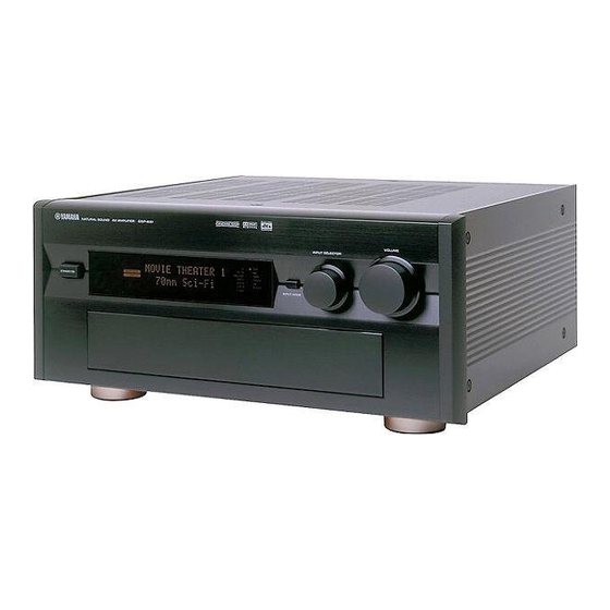
Page 3: Front Panels
DSP-AX1/RX-V1 FRONT PANELS DSP-AX1 RX-V1... -
Page 4: Specifications
DSP-AX1/RX-V1 SPECIFICATIONS AUDIO SECTION Minimum RMS Output Power per Channel Cinema Equalizer MAIN, 20Hz to 20kHz, 0.015% THD, 8Ω ..110W+110W HIgh Frequency ....1kHz to 12.7kHz CENTER, 20Hz to 20kHz, 0.015% THD, 8Ω... - Page 5 DSP-AX1/RX-V1 GENERAL FM SECTION (RX-V1 only) Power Supply Tuning Range U, C models ..... . . AC 120V, 60Hz U, C models ..... . . 87.5 to 107.9MHz A models .
- Page 6 DSP-AX1/RX-V1 SET MENU TABLE SET MENU PRESET VALUE SETTING RANGES SPEAKER SET CENTER SPEAKER LARGE LARGE/SMALL/NONE MAIN SPEAKER LARGE LARGE/SMALL REAR L/R SPEAKER LARGE LARGE/SMALL/NONE REAR CT SPEAKER LARGE LARGE/SMALL/NONE LFE/BASS OUT BOTH SUBWOOFER/MAIN/BOTH FRONT EFCT SPEAKER YES/NONE MAIN LEVEL NORMAL NORMAL/–10dB...
- Page 7 DSP-AX1/RX-V1...
-
Page 8: Internal View
DSP-AX1/RX-V1 INTERNAL VIEW q POWER TRANSFORMER w SUB TRANS P. C. B. (1) e MAIN P. C. B. (4) r VIDEO P. C. B. (4) t VIDEO P. C. B. (1) y SUB TRANS P. C. B. (5) u SUB TRANS P. C. B. (3) i VIDEO P. -
Page 9: Rear Panels
DSP-AX1/RX-V1 4. Removal of DSP P.C.B. (1) Note : a. Remove 2 screws ( u ) and remove the right Plate 1.When the rear panel has been removed, the ground wire of the input/output pin jack becomes loose. Side in Fig. 2. -
Page 10: Self Diagnosis Function
DSP-AX1/RX-V1 SELF DIAGNOSIS FUNCTION This product has a built-in self diagnosis function (DIAG) to facilitate inspection, measurement and determination of a faulty item, if any. There are 14 DIAG menu items each of which has sub-menu items. Listed in the table below are menu items and sub-menu items. - Page 11 DSP-AX1/RX-V1 DIAG menu Sub-menu Remote control code (key) IF STATUS 11. BSI3 --------- 12. BSI4 --------- 13. BSID --------- 14. DIR5 --------- 15. Y918 --------- 16. Y908 --------- 17. DSP6 --------- 18. RAM1 --------- 19. RAM2 --------- DSP RAM CHECK...
- Page 12 DSP-AX1/RX-V1 Display at the start of DIAG The diagnostic menu appears on the monitor screen. (It remains on display until it is canceled.) DIAGNOSTIC MENU 1.DSP THR 8.MAN TST 2.DECODE THR 9.RS232C 3.RAM THR 10.PRESET 4.PRO LOGIC 11.AD DATA 5.DECODE BYP 12.STATUS...
- Page 13 DSP-AX1/RX-V1 In the case where the protection function works after DIAG has been started and the power is turned off ; When the protection function (*2) works, the history of the protection function appears on display and the power turns off. Repair the faulty parts according to the displayed history.
- Page 14 DSP-AX1/RX-V1 Operation procedure of DIAG menu and SUB-MENU There are No.1 to No.14 MENU items and some SUB-MENU items as well. DIAG menu selection DSP-AX1 Main unit: PROGRAM w(forward)/q(reverse) key RX-V1 Main unit: PRESET TUNING + (forward)/-(reverse) key SUB-MENU selection...
- Page 15 DSP-AX1/RX-V1 Details of DIAG menu In each menu, “SPEAKERS” is always set to “LARGE”, D-RANGE to “MAX”, LFE LEVEL to 0dB (-10dB when DOLBY DIGITAL is used) and CENTER DELAY to 0ms unless otherwise specified. 1. DSP THROUGH There are 3 sub menu items (ANALOG BYPS, DSP 0dB, FULL BIT).
- Page 16 DSP-AX1/RX-V1 DSP 0dB [Remote control code: 7A—91 (PRG 10)] The input signal is automatically identified and switched in the priority order of dts > DOLBY DIGITAL > PCM AUDIO > Analog (A/D) according to the signal detection. The L/R, C/LFE, FL/FR, RL/RR, RC signals are output through DSP.
- Page 17 DSP-AX1/RX-V1 2. DECODER THR. The input signal is automatically identified and switched in the priority order of dts > DOLBY DIGITAL > PCM AUDIO > Analog (A/D). There are two sub-menu items (YSS918/908, FULL BIT). This menu is used to check the signal passage of the decoder LSI (YSS918, YSS908).
- Page 18 DSP-AX1/RX-V1 FULL BIT [Remote control code: 7A—10 (TUNER PRESET +)] The head margin is unused and the digital data is output in full bit. The same applies as YSS918/908 except that the digital data is output in full bit at D/A.
- Page 19 DSP-AX1/RX-V1 (In the case of multi-ch source) • AC3D2av outputs signals using DOLBY DIGITAL/dts decode operation. • DSP6#1 outputs the L/R signals to L/R (SD610), RC (SD615, L only), C/LFE to C/LFE (SD611), LSt/ RSt to RLdr/RRdr (SD612). Also, it outputs L/2 + R/2 to FL/FR (SD614) through the external RAM.
- Page 20 DSP-AX1/RX-V1 4. PRO LOGIC The input data is automatically identified in the priority order of PCM > Analog. DTS is inhibited. There are three sub-menu items. Either Pro-logic (auto input balance turned off ) or EFFECT OFF (analog through) is selected.
- Page 21 DSP-AX1/RX-V1 YSS908 [Remote control code: 7A—9D (SET UP)] When the analog, PCM audio or DOLBY DIGITAL 2/0 mode is used, LS, RS, RC signals are pro-logic decoded in YSS908 and output. When the DOLBY DIGITAL mode other than 2/0 is used, the pro logic function does not work and they are muted.
- Page 22 DSP-AX1/RX-V1 5. BYPASS Only PCM and analog modes are used for input signals. The bypassing operation is used according to the menu setting. There are two sub-menu items (DECODER, DSP). This menu is useful when locat- ing the faulty part by bypassing the decoder LSI and DSP6.
- Page 23 DSP-AX1/RX-V1 6. SPEAKERS SET The input signal is automatically identified in the priority order of dts > DOLBY DIGITAL > PCM > Analog. There are seven sub-menu items. The signals output from the DSP are the same as 1. DSP THROUGH: DSP 0dB.
- Page 24 DSP-AX1/RX-V1 7. DISPLAY CHK This program is used to check lighting of the FL display which changes as shown below according to operation of the sub-menu. The signals are processed in the same way as EFFECT OFF of No.4. (The L/R signal is output using ANALOG MAIN BYPASS setting.)
- Page 25 DSP-AX1/RX-V1 8. MANUAL TEST The test noise is output by the noise generator with a built-in DSP through the channels specified by the sub-menu. There are ten sub-menu items. 8. MANUAL TEST ALL [Remote control code: 7A—00 (TAPE PLAY)] Noise is output through all channels.
- Page 26 DSP-AX1/RX-V1 10. PRESET This menu reserves and inhibits initialization of the back-up RAM (parameter, set menu contents, etc. for the sound field program). The input signals are automatically identified in the priority order of AC-3 > PCM > Analog. The signals are processed in the same way as EFFECT OFF of No.4.
- Page 27 DSP-AX1/RX-V1 11. FAN/AD The sub-menu of this menu displays the A/D conversion value of the main CPU (function circuit board IC27) which detects the keys and protection functions of the main unit in %. (100% represents 5V.) It also displays the history of the fan being driven. When in KY0/KY1 page, it is not possible to operate the keys of the main unit because the values of all keys are detected.
- Page 28 DSP-AX1/RX-V1 12. IF STATUS Using this menu, the status data is displayed in the hexadecimal notation one after another. During signal processing, the status before execution of this menu is maintained. If the input mode is analog fixed in the menu before execution, it is necessary to change it to the digital mode according to the following procedure.
- Page 29 DSP-AX1/RX-V1 5th byte Indicates the information on the signal processing status. bit7 MUTE requested bit6 dts flashing bit5 6.1/ES sound field being processed bit4 RF-DEM mute pin bit3 MAIN commands all requested bit2 THROUGH & BYPASS (*2) bit1 6.1/ES AUTO...
- Page 30 DSP-AX1/RX-V1 13. DSP RAM CHECK This menu is used to self-diagnose whether or not the external RAM (IC33, 34, 35) and DSP (IC7, 8) are connected properly, utilizing the CPU -Ext. RAM interface function included in DSP6. During signal processing, the status before execution of this menu is maintained.
-
Page 31: Specifications
DSP-AX1/RX-V1 Software version/compatible version/RS-232C version of main microprocessor 14.SUM/VER/PORT Software version and compatible version of sub-microprocessor M:G38DB/ S:E42D The alphabet of the compatible version represents the communication format compat- ibility between the main and sub microprocessors. If the alphabet representing the com- munication format compatibility agrees, the microprocessors are interchangeable. -
Page 32: Amp Adjustments
DSP-AX1/RX-V1 AMP ADJUSTMENTS IDLING CURRENT ADJUSTMENT Before this adjustment, wait for 10 minutes with no signal applied after the power is turned ON. Item Test Point Adjustment point Rating (DC) MAIN L CB503 VR504 MAIN R CB504 VR505 4.0mV to 12.0mV... -
Page 33: Tuner Adjustments
DSP-AX1/RX-V1 TUNER ADJUSTMENTS (RX-V1 only) Measuring Instruments Dummy antenna FM signal generator (FM SG) FM dummy antenna Stereo signal generator (SSG) 10Ω 45Ω AM signal generator (AM SG) Distortion meter (DIST. M) RECEIVER FM SG (75Ω) (50Ω) AC voltmeter (ACVM) - Page 34 DSP-AX1/RX-V1 FM Adjustment Before Adjustment 1) For dB, 1µV=0dBµ 3) Install the Matching Transformer and connect FM SG. Example : 60dBµ=1mV 4) Set each switch to the following position unless other- 2) 100% modulation means that the frequency deviation is wise specified.
- Page 35 DSP-AX1/RX-V1 Reception Adjusted Rating Step Adjustment item Signal (ANT IN) Test point frequency point Adjustment of 98.1MHz Adjust so that the DC voltage FM ANT (75Ω) Front end IFT Pin 16 of IC1 98.1MHz ± 5kHz front end IFT * (A-4) is maximum.
- Page 36 DSP-AX1/RX-V1 AM Adjustment (This should be done after FM adjustment.) Connection Diagram (Measuring instruments) 1) Adjustment of sensitivity AM loop antenna AM ANT ACVM TUNER AM SG AM SG P. C. B. DIST. M Oscilloscope See page 34 for TP locations & adjustment points.
-
Page 37: Display Data
DSP-AX1/RX-V1 DISPLAY DATA V901 : 32-BT-06G (V4472500) & 0 PATTERN AREA PIN CONNECTION Note 1) F1, F2 ..Filament 3) P1A~P35A, P1B~P35B ..Datum Line 5) IC ....Internal connection 2) NP ....No Pin 4) 1GA~16GA, 1GB~16GB ....Grid 6) Fd terminals are to be supplied through 51kΩ... - Page 38 DSP-AX1/RX-V1 ANODE CONNECTION 37-2...
- Page 39 DSP-AX1/RX-V1 IC DATA IC27 : M30624FGFP (P.C.B. FUNCTION) µ 16 bit -COM (Main CPU) P07/D7 P44/CS0 P06/D6 P45/CS1 P05/D5 P46/CS2 P04/D4 P47/CS3 P03/D3 P50/WRL/WR P02/D2 P51/WRH/BHE P01/D1 P52/RD P00/D0 P53/BCLK P107/AN7/K13 P54/HLDA P106/AN6/K12 P55/HOLD P105/AN5/K11 P56/ALE P104/AN4/K10 P57/RDY/CLKOUT P103/AN3 P60/CTS0/RTS0...
- Page 40 DSP-AX1/RX-V1 IC27 : M30624FGFP (P.C.B. FUNCTION) µ 16 bit -COM (Main CPU) PORT Name Function Power On Power Off Backup TXD2 SDTN SDT for Non Audio TXD1 TXDF FLASH Serial Write Data Transfmission for Flash ROM RXD1 RXDF FLASH Serial Data Receiption for Flash ROM...
- Page 41 DSP-AX1/RX-V1 IC27 : M30624FGFP (P.C.B. FUNCTION) µ 16 bit -COM (Main CPU) PORT Name Function Power On Power Off Backup Power Relay VLRB Volume B VLRA Volume A I Protection MTER Tuner Meter Not used KEY1 Key State 1 KEY0...
- Page 42 DSP-AX1/RX-V1 IC1 : M30624FGFP (P.C.B. DSP) µ 16 bit -COM (Sub CPU) No. PORT Name Function PORT Name Function /CSA2 CS for AC3D2av DSP6 Address Bus 3 /CSA1 CS for AC3Dav DSP6 Address Bus 2 TB4IN DIR5 Double Rate DSP6 Address Bus 1...
- Page 43 DSP-AX1/RX-V1 IC2 : YSD917 (P.C.B. DSP) DIR5 (Digital Format Interface Receiver) AVDD STANDARD SDMCK CLOCK AVSS CLOCK OUTPUT GENERATION SDWCK SYSTEM CLOCK SDBCK GENERATION SELECTION DDIN TEST DDIN SYNC/U /LOCK FS128/C OUTPUT SELECTION ERR/BS DBL/V ERR/BS DBL/V FS128/C DATA BUS...
-
Page 44: Top View
DSP-AX1/RX-V1 IC5 : YSS908-F (P.C.B. DSP) AC3Dav PVSS SDWCK0 SDWCK1 SDBCK0 SDBCK1 SDIA0 SDOB0 SDIA1 SDOB1 RAMA1 SDOB2 RAMA0 RAMA7 RAMWEN RAMA8 RAMOEN RAMA9 TOP VIEW IPORT7 OPORT7 IPORT6 OPORT6 IPORT5 OPORT5 IPORT4 OPORT4 IPORT3 OPORT3 IPORT2 OPORT2 IPORT1 OPORT1... - Page 45 DSP-AX1/RX-V1 IC5 : YSS908 (P.C.B. DSP) AC3Dav Name Function PVDD +5V power supply RAMCEN External SRAM chip enable terminal RAMA16 External SRAM address terminal 16 RAMA15 External SRAM address terminal 15 SDIB0 PCM input terminal 0 to Sub DSP SDIB1...
- Page 46 DSP-AX1/RX-V1 IC5 : YSS908 (P.C.B. DSP) AC3Dav Name Function AC-3 CRC error detect terminal MUTE Auto mute detect terminal KARAOKE AC-3 KARAOKE data detect terminal SURENC AC-3 2/0 mode Dolby surround encode input detect terminal /SDBCK0 SDBCK0 invert clock output terminal...
- Page 47 DSP-AX1/RX-V1 IC6 : YSS918 (P.C.B. DSP) AC3D2av VDD2 SDWCK0 SDWCK1 SDBCK0 SDBCK1 SDIA0 SDOB0 SDIA1 SDOB1 RAMA1 SDOB2 RAMA0 RAMA7 RAMWEN RAMA8 RAMOEN RAMA9 VDD2 VDD2 IPORT7 OPORT7 IPORT6 OPORT6 IPORT5 OPORT5 IPORT4 OPORT4 IPORT3 OPORT3 IPORT2 OPORT2 IPORT1 OPORT1...
- Page 48 DSP-AX1/RX-V1 IC6 : YSS918 (P.C.B. DSP) AC3D2av Name Function +5V power supply (for terminal section) RAMCEN External SRAM chip enable terminal RAMA16 External SRAM address terminal 16 RAMA15 External SRAM address terminal 15 SDIB0 PCM input terminal 0 to Sub DSP...
- Page 49 DSP-AX1/RX-V1 IC6 : YSS918 (P.C.B. DSP) AC3D2av Name Function AC-3 CRC error detect terminal MUTE Auto mute detect terminal KARAOKE AC-3 KARAOKE data detect terminal SURENC AC-3 2/0 mode Dolby surround encode input detect terminal /SDBCK0 SDBCK0 invert clock output terminal...
- Page 50 DSP-AX1/RX-V1 IC7, 8 : YSS910-S DSP6 (Digital Audio Processor) VDD5 VDD5 DB12 DA16 CLOCK DA17 DB11 DA18 DB10 INTERFACE GENERATOR DA19 DB09 DA20 DB08 DA21 DB07 DA22 DB06 DA23 DB05 DB04 CTL-BUS DB03 DA24 DA25 DB02 DA26 DB01 DA27 DB00...
- Page 51 DSP-AX1/RX-V1 IC24 : PM4007A (P.C.B. DSP) AC-3 RF Demodulator AVDD CPIN CMIN AGND DOUT DOUTB WINGT SYST0 SYST1 ADST0 ADST1 BUNRI AGND AVDD Name Function Ground (0V) +5V power supply RESET System resetting terminal (reset at “L”) OSCON Oscillation control terminal. Oscillation ON at “H”, set to “H” normally and to “L” when in standby state...
- Page 52 DSP-AX1/RX-V1 IC24 : PM4007A (P.C.B. DSP) AC-3 RF Demodulator Name Function External RAM address output. Address 6 External RAM address output. Address 7 Ground terminal (0V) +5V power supply External RAM address output. Address 12 External RAM address output. Address 14 (MSB) External RAM write enable signal, active at “L”...
- Page 53 DSP-AX1/RX-V1 IC24 : PM4007A (P.C.B. DSP) AC-3 RF Demodulator Name Function AVDD +5V power supply for analog comparator CPIN Analog comparator input, positive side (Non-reverse side: QPSK input) CMIN Analog comparator input, negative side (reverse side) AGND Ground terminal for analog comparator (0V)
- Page 54 DSP-AX1/RX-V1 IC12 : M35013-079SP (P.C.B. VIDEO) Superimpose TIMING OSC1 VDD1 SIGNAL SEPARATION TUNING SIGNAL OSC2 VERT SELECTOR TUNING OSC IN INPUT (DISPLAY) SIGNAL CONTROL OSC OUT H COUNTER OSCIN DATA ADDRESS DISPLAY CONTROL CONTROL POSITION OSCOUT DETECTOR TIMING TIMING GENERATOR...
-
Page 70: Parts List
DSP-AX1/RX-V1 WARNING Components having special characteristics are marked Z and must be replaced PARTS LIST with parts having specifications equal to those originally installed. Carbon resistors (1/6W or 1/4W) are not included in the ELECTRICAL PARTS ELECTRICAL PARTS List. For the parts No. of the carbon resistors, refer to last page. - Page 71 DSP-AX1/RX-V1 P.C.B. MAIN Schm Schm Ref. PART NO. Description Ref. PART NO. Description V5001000 P.C.B. MAIN(U) * C501 UU167220 C.EL 22uF V5001100 P.C.B. MAIN(C) * C502 UU197470 C.EL 47uF 100V V5001200 P.C.B. MAIN(RT) * C503 UU167220 C.EL 22uF V5001300 P.C.B.
- Page 72 DSP-AX1/RX-V1 P.C.B. MAIN Schm Schm Ref. PART NO. Description Ref. PART NO. Description C554 UT454100 C.PP 0.01uF 100V C743 UA654220 C.MYLAR 0.022uF 50V(UC) C555 UT454100 C.PP 0.01uF 100V C744 FG244220 C.CE 0.022uF 50V(RTABG) C556 VR325300 C.MYLAR 0.047uF 100V C744 UA654220 C.MYLAR 0.022uF...
- Page 73 DSP-AX1/RX-V1 P.C.B. MAIN Schm Schm Ref. PART NO. Description Ref. PART NO. Description D705 VG443500 DIODE.ZENR MTZJ30D 30V Q533 VD488500 TR.DGT DTC143XS D726 iF004600 DIODE 1SS133 Q534 VD488500 TR.DGT DTC143XS F701 VS823100 FUSE 6.0A 125V(UC) Q535 VE198700 TR 2SA1145 O,Y...
- Page 74 DSP-AX1/RX-V1 P.C.B. MAIN Schm Schm Ref. PART NO. Description Ref. PART NO. Description Q703 VS548300 TR 2SB1375 R574 HV455220 R.CAR.FP 220Ω 1/4W R451 VP939700 R.MTL.FLM 4.7Ω R575 HV455220 R.CAR.FP 220Ω 1/4W R452 VP939700 R.MTL.FLM 4.7Ω R576 HV455100 R.CAR.FP 100Ω 1/4W R456 VP939500 R.MTL.FLM...
- Page 75 DSP-AX1/RX-V1 P.C.B. MAIN & VIDEO Schm Schm Ref. PART NO. Description Ref. PART NO. Description R637 HV453470 R.CAR.FP 4.7Ω 1/4W VK697600 SCR.BND.HD 3x10 SP ZMC2-Y R640 VK188400 R.FUS 330Ω 1/4W R641 HZ003780 R.MTL.PLAT 0.22Ω+0.22 5W R643 HV453470 R.CAR.FP 4.7Ω 1/4W R646 HV453470 R.CAR.FP...
- Page 76 DSP-AX1/RX-V1 P.C.B. VIDEO Schm Schm Ref. PART NO. Description Ref. PART NO. Description UB245100 C.CE.M.CHP 0.1uF * C202 VZ001600 C.MYLAR 0.047pF * C30 UU127470 C.EL 47uF * C203 VZ001600 C.MYLAR 0.047pF * C31 UU127470 C.EL 47uF * C204 VZ001600 C.MYLAR 0.047pF...
- Page 77 DSP-AX1/RX-V1 P.C.B. VIDEO Schm Schm Ref. PART NO. Description Ref. PART NO. Description C932 VR169200 C.MYLAR.ML ECQ-V1H474JL3 * JK261 V4164400 JACK.PHONE YKB21-5209 * C934 UU147100 C.EL 10uF JK381 V2589500 CN C935 UT452470 C.PP 470pF 100V V2725700 COIL 15uH C936 UT452470 C.PP...
- Page 78 DSP-AX1/RX-V1 P.C.B. VIDEO Schm Schm Ref. PART NO. Description Ref. PART NO. Description Q918 VZ725900 TR 2SD1938F S,T R957 Vi194100 R.MTL.CHP 470Ω 1/10W Q919 VZ725900 TR 2SD1938F S,T R961 Vi194100 R.MTL.CHP 470Ω 1/10W Q920 VZ725900 TR 2SD1938F S,T R963 Vi194100 R.MTL.CHP...
- Page 79 DSP-AX1/RX-V1 P.C.B. SUB TRANS Schm Schm Ref. PART NO. Description Ref. PART NO. Description V5002100 P.C.B. SUB TRANS.(U) C757 Vi716700 C.MYLAR 0.01uF 50V(RT) V5002200 P.C.B. SUB TRANS.(C) C758 VV975400 C.CE 0.01uF 275V V5002300 P.C.B. SUB TRANS.(RT) C759 VV975400 C.CE 0.01uF 275V(C) V5002400 P.C.B.
- Page 80 DSP-AX1/RX-V1 P.C.B. SUB TRANS Schm Schm Ref. PART NO. Description Ref. PART NO. Description * C856 UU137220 C.EL 22uF Q817 iC1815C0 TR 2SC1815 Y D481 VR253700 DIODE.BRG S1NB20 1.0A 200V Q818 iA097000 2SA970 GR,BL * D482 V4870400 DIODE.BRG D4SBS4 4.0A...
- Page 81 DSP-AX1/RX-V1 P.C.B. FUNCTION Schm Schm Ref. PART NO. Description Ref. PART NO. Description V5002600 P.C.B. FUNCTION(UC) * C35 UU166470 C.EL 4.7uF V5002700 P.C.B. FUNCTION(RT) UP652470 C.POL 470pF 100V V5002800 P.C.B. FUNCTION(A) UP652470 C.POL 470pF 100V V5002900 P.C.B. FUNCTION(BG) * C38 UU147100 C.EL...
- Page 82 DSP-AX1/RX-V1 P.C.B. FUNCTION Schm Schm Ref. PART NO. Description Ref. PART NO. Description * C88 UU137220 C.EL 22uF C144 UB245100 C.CE.M.CHP 0.1uF UP654270 C.POL 0.027uF 100V C145 UB245100 C.CE.M.CHP 0.1uF UP654270 C.POL 0.027uF 100V C146 UB245100 C.CE.M.CHP 0.1uF * C91 UU137220 C.EL...
- Page 83 DSP-AX1/RX-V1 P.C.B. FUNCTION Schm Schm Ref. PART NO. Description Ref. PART NO. Description * C207 UU166220 C.EL 2.2uF XF291A00 IC uPC4570G2 * C208 UU166220 C.EL 2.2uF XF291A00 IC uPC4570G2 * C211 UU119100 C.EL 1000uF 6.3V XF291A00 IC uPC4570G2 C212 UB245100 C.CE.M.CHP 0.1uF...
- Page 84 DSP-AX1/RX-V1 P.C.B. FUNCTION Schm Schm Ref. PART NO. Description Ref. PART NO. Description iA103700 TR.CHP 2SA1037 Q,R,S Vi196600 R.MTL.CHP 4.7KΩ 1/10W iA103700 TR.CHP 2SA1037 Q,R,S Vi200000 R.MTL.CHP 100KΩ 1/10W VD303700 TR 2SC3326 A,B Vi196100 R.MTL.CHP 3.3KΩ 1/10W VP872700 TR 2SC4488 S,T Vi197200 R.MTL.CHP...
- Page 85 DSP-AX1/RX-V1 P.C.B. FUNCTION Schm Schm Ref. PART NO. Description Ref. PART NO. Description R125 Vi192500 R.MTL.CHP 100Ω 1/10W R182 Vi196100 R.MTL.CHP 3.3KΩ 1/10W R126 HV453220 R.CAR.FP 2.2Ω 1/4W R183 VK583400 R.MTL.CHP 1MΩ 1/10W R127 Vi199000 R.MTL.CHP 47KΩ 1/10W R184 Vi196100 R.MTL.CHP...
- Page 86 DSP-AX1/RX-V1 P.C.B. FUNCTION Schm Schm Ref. PART NO. Description Ref. PART NO. Description R240 Vi191700 R.MTL.CHP 47Ω 1/10W R300 Vi191700 R.MTL.CHP 47Ω 1/10W R241 Vi191700 R.MTL.CHP 47Ω 1/10W R301 VK583400 R.MTL.CHP 1MΩ 1/10W R242 Vi200000 R.MTL.CHP 100KΩ 1/10W R302 VK583400 R.MTL.CHP 1MΩ...
- Page 87 DSP-AX1/RX-V1 P.C.B. DSP Schm Schm Ref. PART NO. Description Ref. PART NO. Description V5003000 P.C.B. DSP(RBGT) UB044220 C.CE.M.CHP 0.022uF V5003100 P.C.B. DSP(UA) UB245100 C.CE.M.CHP 0.1uF V5003200 P.C.B. DSP(C) UB051100 C.CE.M.CHP 10pF * CB1 V4707900 CN.FBRSNSR 1P GP1F37R1 UB245100 C.CE.M.CHP 0.1uF * CB2 V4707900 CN.FBRSNSR 1P GP1F37R1...
- Page 88 DSP-AX1/RX-V1 P.C.B. DSP Schm Schm Ref. PART NO. Description Ref. PART NO. Description VJ900700 C.CE.M.CHP 33pF * C163 UU137470 C.EL 47uF VJ900700 C.CE.M.CHP 33pF * C164 UU137470 C.EL 47uF UB245100 C.CE.M.CHP 0.1uF C165 VQ645600 C.MYLAR 100pF * C88 UU128100 C.EL...
- Page 89 DSP-AX1/RX-V1 P.C.B. DSP Schm Schm Ref. PART NO. Description Ref. PART NO. Description * C216 Vi717000 C.MYLAR 0.018uF * C269 UU137470 C.EL 47uF * C217 UU118330 C.EL 330uF 6.3V * C270 UU128100 C.EL 100uF C218 UB245100 C.CE.M.CHP 0.1uF * C271 UU128100 C.EL...
- Page 90 DSP-AX1/RX-V1 P.C.B. DSP Schm Schm Ref. PART NO. Description Ref. PART NO. Description * C323 UU137470 C.EL 47uF * C376 Vi717000 C.MYLAR 0.018uF C324 UB245100 C.CE.M.CHP 0.1uF C381 UB051470 C.CE.M.CHP 47pF C325 UB245100 C.CE.M.CHP 0.1uF C382 UB051470 C.CE.M.CHP 47pF * C326 UU137470 C.EL...
- Page 91 DSP-AX1/RX-V1 P.C.B. DSP Schm Schm Ref. PART NO. Description Ref. PART NO. Description C433 UB245100 C.CE.M.CHP 0.1uF * IC2 XW526A00 IC YSD917 * C434 UU128100 C.EL 100uF * IC3 XW272A00 IC AK5383-VS C901 VH053100 C.CE.TUBLR 0.1uF XP250A00 IC HD74HC00FPTR NAND C902 VH053100 C.CE.TUBLR 0.1uF...
- Page 92 DSP-AX1/RX-V1 P.C.B. DSP Schm Schm Ref. PART NO. Description Ref. PART NO. Description V2726500 COIL 68uH R138 Vi195900 R.MTL.CHP 2.7KΩ 1/10W V2726500 COIL 68uH R139 HV454220 R.CAR.FP 22Ω 1/4W V2726500 COIL 68uH R141 Vi200000 R.MTL.CHP 100KΩ 1/10W V2726500 COIL 68uH...
- Page 93 DSP-AX1/RX-V1 P.C.B. DSP Schm Schm Ref. PART NO. Description Ref. PART NO. Description R195 Vi196500 R.MTL.CHP 4.3KΩ 1/10W R196 Vi200000 R.MTL.CHP 100KΩ 1/10W R197 Vi194900 R.MTL.CHP 1KΩ 1/10W R198 Vi194900 R.MTL.CHP 1KΩ 1/10W R199 Vi194900 R.MTL.CHP 1KΩ 1/10W R200 HV454220 R.CAR.FP 22Ω...
- Page 94 DSP-AX1/RX-V1 P.C.B. TUNER (Lead Type) Schm Schm Ref. PART NO. Description Ref. PART NO. Description V2518600 P.C.B. TUNER/TU-01(UC) VD631600 DIODE 1SS133,176,HSS104 V2518800 P.C.B. TUNER/TU-01(A) VG437700 DIODE.ZENR MTZJ5.6B 5.6V VQ961900 CN GG000560 FLTR.CE SFE10.7MS3GHY-A VG288900 C.EL 100uF GG000560 FLTR.CE SFE10.7MS3GHY-A(UC VG275800 C.CE.TUBLR 8.2pF * Fi2 V4545200 FLTR.CE...
- Page 95 DSP-AX1/RX-V1 P.C.B. TUNER (Lead Type & SMD) Schm Schm Ref. PART NO. Description Ref. PART NO. Description V2519300 P.C.B.CHP TUNER/TU-01(UC) UR837470 C.EL 47uF V2519500 P.C.B.CHP TUNER/TU-01(A) UR837470 C.EL 47uF VG287600 C.EL 100uF UR837470 C.EL 47uF UB050800 C.CE.M.CHP 8pF VA761100 C.CE 27pF UR837470 C.EL...