Table of Contents
Advertisement
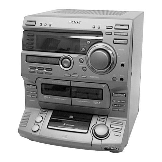
HCD-DR8AV/W900AV
SERVICE MANUAL
Ver 1.1 2003. 05
HCD-DR8AV/W900AV is the tuner, deck, CD and
amplifier section in LBT-DR8AV/W900AV.
Amplifier section
LBT-W900AV
Front Speaker:
Continuous RMS power output (Reference)
100 + 100W
(8 Ω at 1 kHz, 10% THD)
Total harmonics distortion
Less than 0.07%
(8 Ω at 1 kHz, 50W)
Center Speaker:
Continuous RMS power output (Reference)
45W
(8 Ω at 1 kHz, 10% THD)
Rear Speaker:
Continuous RMS power output (Reference)
40 + 40W
(8 Ω at 1 kHz, 10% THD)
LBT-DR8AV
Front Speaker:
The following measured at AC 120/220/240V, 50Hz
DIN power output (Rated)
130 + 130W
(6 Ω at 1 kHz, DIN)
Continuous RMS power output (Reference)
160 +160W
(6 Ω at 1 kHz, 10% THD)
Center Speaker:
DIN power output (Rated)
30W
(8 Ω at 1 kHz, DIN)
Continuous RMS power output (Reference)
40W
(8 Ω at 1 kHz, 10% THD)
Sony Corporation
9-928-902-12
2003E16-1
Home Audio Company
© 2003.05
Published by Sony Engineering Corporation
Photo: HCD-DR8AV
Model Name Using Similar Mechanism
CD
CD Mechanism Type
Section
Base Unit Name
Optical Pick-up Name
Model Name Using Similar Mechanism
Tape deck
Section
Tape Transport Mechanism Type
SPECIFICATIONS
Rear Speaker:
DIN power output (Rated)
30 + 30W
(8 Ω at 1 kHz, DIN)
Continuous RMS power output (Reference)
40 + 40W
(8 Ω at 1 kHz, 10%
THD)
Inputs
PHONO IN (phono jacks):
sensitivity 3mV,
impedance 47k Ω
MIX MIC (phone jack):
sensitivity 1mV,
impedance 10k Ω
VIDEO1 IN (phono jacks):
sensitivity 250mV,
impedance 47k Ω
VIDEO2 IN (phono jacks):
sensitivity 250mV,
impedance 47k Ω
MD IN (phono jacks):
sensitivity 450mV,
impedance 47k Ω
(LBT-DR8AV/W900AV)
DVD IN (phono jacks):
sensitivity 450mV,
impedance 47kΩ
Outputs
PHONES (stereo phone jack):
accepts headphones of 8
Ω or more
VIDEO OUT (phono jack):
voltage 250mV,
impedance 1k Ω
COMPACT DISC DECK RECEIVER
US Model
Canadian Model
HCD-W900AV
E Model
Australian Model
HCD-DR8AV
HCD-DR4/DR5/DR6/DR440/
W300/W5000/XB500
CDM37M-5BD32L
BU-5BD32L
KSS-213D/Q-N
NEW
TCM-230AWR2/230PWR2
MD OUT (phono jacks):
voltage 250mV, impedance
1k Ω
WOOFER OUT (phono jack):
voltage 1V, impedance
1k Ω
FRONT SPEAKER:
(LBT-W900AV)
accepts impedance of 8 to
16 Ω
(LBT-DR8AV)
accepts impedance of 6 to
16 Ω
CENTER SPEAKER:
accepts impedance of 8 to
16 Ω
REAR SPEAKER:
accepts impedance of 8 to
16 Ω
Video section
Inputs
VIDEO1 IN (phono jacks):
1Vp-p, 75 Ω
VIDEO2 IN (phono jacks):
1Vp-p, 75 Ω
Output
1Vp-p, 75 Ω
VIDEO OUT (phono jack):
— Continued on next page —
Advertisement
Table of Contents

Related Manuals for Sony HCD-DR8AV


Summary of Contents for Sony HCD-DR8AV
- Page 1 SERVICE MANUAL US Model Canadian Model Ver 1.1 2003. 05 HCD-W900AV E Model Australian Model HCD-DR8AV HCD-DR8AV/W900AV is the tuner, deck, CD and Photo: HCD-DR8AV amplifier section in LBT-DR8AV/W900AV. HCD-DR4/DR5/DR6/DR440/ Model Name Using Similar Mechanism W300/W5000/XB500 CD Mechanism Type CDM37M-5BD32L...
- Page 2 4-track 2-channel stereo Speaker cords (2) Frequency response (DOLBY NR OFF) 40 – 13,000Hz (±3dB), Design and specifications are subject to change without notice. using a Sony TYPE I cassette 40 – 14,000Hz (±3dB), using a Sony TYPE II cassette...
-
Page 3: Leakage Test
CRITIQUES POUR LA SÉCURITÉ DE FONCTIONNEMENT . NE COMPONENTS WITH SONY PARTS WHOSE PART NUMBERS REMPLACER CES COMPOSANTS Q UE PAR DES PIÈSES SONY APPEAR AS SHOWN IN THIS MANUAL OR IN SUPPLEMENTS DONT LES NUMÉROS SONT DONNÉS D ANS CE MANUEL OU PUBLISHED BY SONY. -
Page 4: Servicing Note
SECTION 1 SERVICING NOTE About CD-TEXT display NOTES ON HANDLING THE OPTICAL PICK-UP BLOCK This unit is provided with a simple CD-TEXT display function. OR BASE UNIT The CD-TEXT contents of 20 tracks are displayed on the fluorescent display tube. The laser diode in the optical pick-up block may suffer electrostatic Since the function is simple, some special characters may not be break-down because of the potential difference generated by the... -
Page 5: Table Of Contents
TABLE OF CONTENTS 1. SERVICING NOTE 7-15. Printed Wiring Board Power Section ·························································· 4 (DR8AV model) ································································ 61 7-16. Schematic Diagram Power (1/2) Section 2. GENERAL ·········································································· 6 (W900AV model) ····························································· 63 7-17. Schematic Diagram Power (2/2) Section 3. DISASSEMBLY (W900AV model) ·····························································... -
Page 6: General
SECTION 2 GENERAL Front Panel 0!¡ !™ !£ !¢ !∞ !§ &¡ &º !¶ ^ª ^• !• !ª ^¶ @º @¡ ^§ ^∞ ^¢ @™ @£ ^£ ^™ ^¡ @¢ ^º %ª @∞ @§ %• %¶ %§ @¶ @• @ª #º#¡... - Page 7 This section is extracted from instruction manual. — 7 —...
-
Page 8: Disassembly
(HCD-W900AV) !¢ Back panel 2 Two screws (BVTP 3x8) !£ Power cord 9 Four screws (BVTP 3x8) 0 Two screws (BVTP 3x8) (HCD-DR8AV) 8 Five screws (BVTP 3x8) 7 Seven screws (BVTP 3x8) !§ Main board 6 Connector (CN903) (HCD-DR8AV) 1 Flat type wire (CN1) !¡... -
Page 9: Sub Panel
3-3. SUB PANEL 7 Three screws (BVTP 2.6x8) 6 Two screws (BVTP 2.6x8) 4 Two screws (BTP 2.6x6) 1 Two screws (BVTP 2.6x8) 3 Open the CD lid assembly 2 Front input board 9 Two screws (BVTP 2.6x8) 0 Bracket (CD-R2) 5 Screw (BVTP 3x8) 8 Sub panel block 3-4. -
Page 10: Tape Mechanism Deck And Cassette Lid
3-5. TAPE MECHANISM DECK AND CASSETTE LID 1 Three screws (BVTP 2.6x8) Claw Holder assembly 8 Torsion spring (TC-A) Claw 6 Holder (A) assembly 2 Three screws (Refer to lower figure) (BVTP 2.6x8) Claw Cassette lid assembly Claw 3 Tape mechanism Portion B 9 Torsion spring (TC-B) 4 Cassette lid (A) assembly... -
Page 11: Disc Table
3-8. DISC TABLE Note: When the disc table is installed, adjust the positions of roller cam and mark ” as shown in the figure, then set to the groove of disc table. Stop screw Screw (BVTP3X8) Screw (BVTP3X8) Bracket (BU) Disc table —... -
Page 12: Service Mode
SECTION 4 SERVICE MODE MC Cold Reset • The cold reset clears all data including preset data stored in the RAM to initial conditions. Execute this mode when returning the set to the customer. Procedure: 1. Press three buttons t/CLOCK SET , ENTER , and 1/u simultaneously. 2. - Page 13 AMS Test Mode • This mode is used for checking the AMS operations of the tape deck. 7-819-039-12 Alignment tape, AMS-110A Procedure: 1. Press the 1/u button to turn the set ON. 2. Set the tape (AMS-110A). 3. Press the three buttons t/CLOCK SET , ENTER , and DISC 3 button simultaneously. 4.
- Page 14 • Display when ended abnormally When the tape deck is abnormal: The state when ended abnormally is displayed. The contents of display are the same as that during aging. When the CD player is abnormal: A message indicating that errors such as “CD MEC ERR” have occurred. Check the error contents in the following error history display mode.
-
Page 15: Mechanical Adjustments
SECTION 5 SECTION 6 MECHANICAL ADJUSTMENTS ELECTRICAL ADJUSTMENTS Precaution DECK SECTION 0 dB=0.775V Clean the following parts with a denatured alcohol-moistened swab: Demagnetize the record/playback head with a head record/playback heads pinch rollers demagnetizer. erase head rubber belts Do not use a magnetized screwdriver for the adjustments. capstan idlers After the adjustments, apply suitable locking compound to the... - Page 16 Mode: Playback Tape Speed Adjustment (Deck A) test tape Note: Set the test mode using the following method and begin tape P-4-A100 speed adjustment. (10kHz, –10dB) oscilloscope In the test mode, the speed will switch to double speed or normal speed each time the HI-SPEED DUB button is pressed. MD OUT Procedure: With the power turned ON, press the t/CLOCK SET button,...
- Page 17 Record Bias Adjustment (Deck B) Record Level Adjustment (Deck B) Procedure: Procedure: INTRODUCTION INTRODUCTION When set to the test mode performed in Tape Speed Adjustment, When set to the test mode performed in Tape Speed Adjustment, when the tape is rewound after recording, the “REC memory mode” when the tape is rewound after recording, the “REC memory mode”...
- Page 18 Note: Clear RF signal waveform means that the shape “ ” can be CD SECTION clearly distinguished at the center of the waveform. Note: RF signal waveform CD Block is basically constructed to operate without VOLT/DIV : 200mV TIME/DIV : 500ns adjustment.
-
Page 19: Diagrams
HCD-DR8AV/W900AV SECTION 7 DIAGRAMS 7-1. CIRCUIT BOARDS LOCATION SURROUND AMP board FL board TUNER UNIT JACK board TC-A board TC-B board PANEL VR board SUB TRANS board FRONT INPUT board (W900AV) TRANS board LED (PANEL) board MAIN board CD-L board... -
Page 20: Block Diagrams
HCD-DR8AV/W900AV 7-2. BLOCK DIAGRAMS BD SECTION OPTICAL PICK-UP BLOCK (KSS-213D/Q-NP) IC101 XTAI DETECTOR DIGITAL SERVO TIMING X101 IC103 DIGITAL SIGNAL PROCESSOR LOGIC 16.9344MHz RF AMP ERROR XTAO CORRECTOR RF EQ RF AC DIGITAL D OUT SUMMING DOUT DEMODULATION INTERFACE FOCUS... -
Page 21: Deck Section
HCD-DR8AV/W900AV DECK SECTION PB A/B S1004 S1008 MS OUT B CrO A CrO CN301 R CH RV311 28 27 PLAYBACK IC611 PB-A/B A 120/70 B NORM/CROM/METAL LEVEL DECK A A IN PB OUT B IN TC PB L HP101 PB HEAD... -
Page 22: Main (1/2) Section
HCD-DR8AV/W900AV MAIN (1/2) SECTION AV SWITCH IC191 J804 J702 VIDEO 2 VIDEO VD OUT SOUND PROCESSOR 1 J702 IC101 J701 DVD VIDEO REC B2 MD OUT J702 VIDEO 1 DECK SECTION REC A2 TC REC L (Page 24) IC601 PHONO AMP... -
Page 23: Main (2/2) Section
HCD-DR8AV/W900AV MAIN (2/2) SECTION DR8AV ONLY FAN901 PL-RELAY FAN SWITCH Q961, 962 POWER IC931 Q931 SECTION POWER SWITCH MAIN CONTROL SECTION (Page 29, 31) +10V IC501 (2/2) +UNREG, 17V PL A+10V (Page 29, 31) ST +10V STK-POWER STK POWER Q932... -
Page 24: Power Section (Dr8Av Model)
HCD-DR8AV/W900AV POWER SECTION (DR8AV model) MIC AMP MIC VOLUME MIC AMP IC850 (1/2) RV850 IC850 (2/2) J801 MAIN 1 MIX MIC SECTION MIC-SIG (Page 25) MAIN 1 DISPLAY RELAY SECTION MIC-SIG F-RELAY SECTION DRIVER POWER AMP & VOLUME CONTROL (Page 26) -
Page 25: Power Section (W900Av Model)
HCD-DR8AV/W900AV POWER SECTION (W900AV model) MIC AMP MIC VOLUME MIC AMP IC850 (1/2) RV850 IC850 (2/2) J801 MAIN 1 SECTION MIX MIC MIC-SIG (Page 25) MAIN 1 DISPLAY RELAY SECTION F-RELAY MIC-SIG SECTION DRIVER POWER AMP & VOLUME CONTROL (Page 26) - Page 26 HCD-DR8AV/W900AV DISPLAY SECTION Q602 LED POWER LED5V Q603 SWITCH D632 D641 LED POWER D635 D631 DISPLAY CONTROL LED5V SWITCH D637 D636 IC601 D611 D638 D700 D614 D612 Q601 D616 D613 SWITCH D618 D617 LED SEL D621 D620 SERIAL D623 D619...
- Page 27 HCD-DR8AV/W900AV Waveforms – MAIN (2/5) Section – THIS NOTE IS COMMON FOR PRINTED WIRING – BD SECTION – BOARDS AND SCHEMATIC DIAGRAMS. (In addition to this, the necessary note is printed in each block.) 5.5Vp-p 3.1Vp-p For schematic diagrams. 16MHz Note: IC501 !£...
-
Page 28: Printed Wiring Board Bd Section
HCD-DR8AV/W900AV 7-3. PRINTED WIRING BOARD BD SECTION • Refer to page 19 for Circuit Boards Location. (VC) (RP) (AGCCON) (FE) (TE) (FF1) (Page 42) — 37 — — 38 —... - Page 29 HCD-DR8AV/W900AV 7-4. SCHEMATIC DIAGRAM BD SECTION • Refer to page 36 for Waveforms. (TE) (FE) (RP) TP (AGCCON) (VC) (Page 48) The components identified by Les composants identifiés par mark ! or dotted line with mark une marque ! sont critiques ! are critical for safety.
- Page 30 HCD-DR8AV/W900AV • Semiconductor Location • Refer to page 19 for Circuit Boards Location. 7-5. PRINTED WIRING BOARD MAIN SECTION Ref. No. Location (Page 101) D333 DVD INPUT D334 FRONT REAR WOOFER D335 M901 CD DIGITAL VIDEO CENTER WOOFER D336 C732...
-
Page 31: Schematic Diagram Main (1/5) Section
HCD-DR8AV/W900AV • Refer to page 103 for IC Block Diagrams. 7-6. SCHEMATIC DIAGRAM MAIN (1/5) SECTION — 43 — — 44 —... -
Page 32: Schematic Diagram Main (2/5) Section
HCD-DR8AV/W900AV 7-7. SCHEMATIC DIAGRAM MAIN (2/5) SECTION • Refer to page 36 for Waveforms. • Refer to page 41 for Printed Wiring Board. • Refer to page 104 for IC Pin Functions. (Page 51) (Page 44) (Page 52) (Page 70) -
Page 33: Schematic Diagram Main (3/5) Section
HCD-DR8AV/W900AV 7-8. SCHEMATIC DIAGRAM MAIN (3/5) SECTION • Refer to page 41 for Printed Wiring Board. (Page 46) (Page 45, 46) CD DIGITAL (Page 39) (Page 86) (Page 49) (Page (Page 44) — 47 — — 48 —... -
Page 34: Schematic Diagram Main (4/5) Section
HCD-DR8AV/W900AV 7-9. SCHEMATIC DIAGRAM MAIN (4/5) SECTION • Refer to page 41 for Printed Wiring Board. (Page 44) (Page 54) (Page 100) (Page 51) (Page 47) (Page 45) — 49 — — 50 —... -
Page 35: Schematic Diagram Main (5/5) Section
HCD-DR8AV/W900AV 7-10. SCHEMATIC DIAGRAM MAIN (5/5) SECTION • Refer to page 41 for Printed Wiring Board. M5F7805L (Page (Page DR8AV (Page 90) (Page (Page 44) (Page 46) (Page DR8AV: NJM7812FA W900AV: M5F78M12 M901 DR8AV (Page 57, 65) (Page 57, 65) —... -
Page 36: Schematic Diagram Deck Section
HCD-DR8AV/W900AV 7-11. SCHEMATIC DIAGRAM DECK SECTION (Page 49) The components identified by Les composants identifiés par mark ! or dotted line with mark une marque ! sont critiques ! are critical for safety. pour la sécurité. Replace only with part number Ne les remplacer que par une specified. -
Page 37: Printed Wiring Board Deck Section
HCD-DR8AV/W900AV 7-12. PRINTED WIRING BOARD DECK SECTION • Refer to page 19 for Circuit Boards Location. (Page 41) — 55 — — 56 —... - Page 38 HCD-DR8AV/W900AV 7-13. SCHEMATIC DIAGRAM POWER (1/2) SECTION (DR8AV model) • Refer to page 61 for Printed Wiring Board. (Page 97) C891 C841 3300 3300 IC801 STK411-230M 2CH CLASS AB + VOL CONTROL C892 C842 3300 3300 THERMAL (Page 52) R858 R808 0.22...
- Page 39 HCD-DR8AV/W900AV 7-14. SCHEMATIC DIAGRAM POWER (2/2) SECTION (DR8AV model) • Refer to page 61 for Printed Wiring Board. The components identified by Les composants identifiés par (Page 57) (Page 57) (Page 58) mark ! or dotted line with mark une marque ! sont critiques ! are critical for safety.
-
Page 40: Printed Wiring Board Power Section
HCD-DR8AV/W900AV 7-15. PRINTED WIRING BOARD POWER SECTION (DR8AV model) • Refer to page 19 for Circuit Boards Location. SORROUND SPEAKER REAR CENTER • Semiconductor Location Ref. No. Location D401 D402 D403 D405 D406 D409 D801 D802 D803 D823 D831 D833... - Page 41 HCD-DR8AV/W900AV 7-16. PRINTED WIRING BOARD POWER SECTION (W900AV model) • Refer to page 19 for Circuit Boards Location. SORROUND SPEAKER CENTER • Semiconductor REAR Location Ref. No. Location D401 D402 D403 D405 D406 D801 D803 D804 D805 D831 D833 D834...
-
Page 42: Schematic Diagram Power (1/2) Section
HCD-DR8AV/W900AV 7-17. SCHEMATIC DIAGRAM POWER (1/2) SECTION (W900AV model) • Refer to page 63 for Printed Wiring Board. (Page 93) 2CH CLASS AB +VOL CONTROL 4700 4700 JW804 (Page R858 0.22 R808 0.22 (Page (Page The components identified by Les composants identifiés par... - Page 43 HCD-DR8AV/W900AV 7-18. SCHEMATIC DIAGRAM POWER (2/2) SECTION (W900AV model) • Refer to page 63 for Printed Wiring Board. (Page 65) (Page 66) (Page 94) (Page 102) The components identified by Les composants identifiés par mark ! or dotted line with mark une marque ! sont critiques ! are critical for safety.
-
Page 44: Schematic Diagram Power (2/2) Section
HCD-DR8AV/W900AV • Refer to page 103 for IC Block Diagrams. • Refer to page 106 for IC Pin Functions. 7-19. SCHEMATIC DIAGRAM FL SECTION (Page 77) (Page (Page 77) (Page 46) DR8AV MODEL (Page 73) — 69 — — 70 —... -
Page 45: Fl Section
HCD-DR8AV/W900AV 7-20. PRINTED WIRING BOARD FL SECTION • Refer to page 19 for Circuit Boards Location. (Page 41) DR8AV MODEL (Page 79) (Page 80) (Page 75) (Page 79) • Semiconductor Location Ref. No. Location Ref. No. Location D601 A-13 Q601... -
Page 46: Schematic Diagram Panel Vr Section
HCD-DR8AV/W900AV 7-21. SCHEMATIC DIAGRAM PANEL VR SECTION • Refer to page 103 for IC Block Diagrams. 5.1CH 5.1CH (Page 70) — 73 — — 74 —... -
Page 47: Panel Vr Section
HCD-DR8AV/W900AV 7-22. PRINTED WIRING BOARD PANEL VR SECTION • Refer to page 19 for Circuit Boards Location. DVD 5.1CH LOGIC (Page 71) • Semiconductor Location Ref. No. Location D611 D612 D613 D616 D617 D-10 D618 D-11 D619 D620 D621 D623... -
Page 48: Schematic Diagram Tc Panel Section
HCD-DR8AV/W900AV 7-23. SCHEMATIC DIAGRAM TC PANEL SECTION (Page 70) (Page 69) (Page 82) (Page 81, 82) (Page 70) — 77 — — 78 —... -
Page 49: Printed Wiring Board Tc Panel Section
HCD-DR8AV/W900AV • Refer to page 19 for Circuit Boards Location. 7-24. PRINTED WIRING BOARD TC PANEL SECTION (Page 71) (Page 72) (Page 83) (Page 71) (Page 84) — 79 — — 80 —... -
Page 50: Schematic Diagram Cd Panel Section
HCD-DR8AV/W900AV 7-25. SCHEMATIC DIAGRAM CD PANEL SECTION (Page 78) (Page 77, 78) (Page 43) — 81 — — 82 —... -
Page 51: Printed Wiring Board Cd Panel Section
HCD-DR8AV/W900AV 7-26. PRINTED WIRING BOARD CD PANEL SECTION • Refer to page 19 for Circuit Boards Location. (Page 80) (Page 79) (Page — 83 — — 84 —... -
Page 52: Schematic Diagram Cd Motor Section
HCD-DR8AV/W900AV 7-27. SCHEMATIC DIAGRAM CD MOTOR SECTION (Page 48) — 85 — — 86 —... -
Page 53: Printed Wiring Board Cd Motor Section
HCD-DR8AV/W900AV 7-28. PRINTED WIRING BOARD CD MOTOR SECTION • Refer to page 19 for Circuit Boards Location. (Page 42) — 87 — — 88 —... -
Page 54: Schematic Diagram Jack Section
HCD-DR8AV/W900AV 7-29. SCHEMATIC DIAGRAM JACK SECTION (Page 57, 65) (Page 52) — 89 — — 90 —... -
Page 55: Printed Wiring Board Jack Section
HCD-DR8AV/W900AV • Refer to page 19 for Circuit Boards Location. 7-30. PRINTED WIRING BOARD JACK SECTION (Page 41) (Page 61, 63) — 91 — — 92 —... -
Page 56: Schematic Diagram Trans Section
HCD-DR8AV/W900AV 7-31. SCHEMATIC DIAGRAM TRANS SECTION (W900AV model) (Page 65) (Page 67) R961 3.3M 1/2W The components identified by Les composants identifiés par mark ! or dotted line with mark une marque ! sont critiques ! are critical for safety. -
Page 57: Printed Wiring Board Trans Section
HCD-DR8AV/W900AV 7-32. PRINTED WIRING BOARD TRANS SECTION (W900AV model) • Refer to page 19 for Circuit Boards Location. (Page 64) (Page — 95 — — 96 —... -
Page 58: Schematic Diagram
HCD-DR8AV/W900AV 7-33. SCHEMATIC DIAGRAM TRANS SECTION (DR8AV model) 0.22 AUS MODEL 0.22 E,EA,AR,SP MODEL E,EA,AR,SP MODEL JW971 E,EA,AR,SP MODEL (Page 57) JW965 JW966 MX MODEL The components identified by Les composants identifiés par mark ! or dotted line with mark une marque ! sont critiques ! are critical for safety. -
Page 59: Leaf Sw Section
HCD-DR8AV/W900AV 7-34. PRINTED WIRING BOARD TRANS SECTION (DR8AV model) • Refer to page 19 for Circuit Boards Location. 7-35. SCHEMATIC DIAGRAM LEAF SW SECTION E, EA AR, SP MODEL E, EA AR, SP MODEL JW965 JW966 JW967 MX MODEL EXCEPT AUS, MX (Page 49) 7-36. -
Page 60: Surround Section
HCD-DR8AV/W900AV 7-37. Schematic Diagram – SURROUND Section – (Page (Page 59, 67, 68) The components identified by Les composants identifiés par mark ! or dotted line with mark une marque ! sont critiques ! are critical for safety. pour la sécurité. -
Page 61: Ic Block Diagrams
7-39. IC BLOCK DIAGRAMS • MAIN (1/5) section • PANEL FL section IC181 MC14052BF IC603 BA3830F REFFERENCE 18 RESET RESET CURRENT REFFERENCE 17 f01 2XCOM CURRENT XCOM LINE 16 f02 LINE 15 f03 13 f05 IC191 BA7615N RESET 12 f06 MUTE BIAS 11 REC... -
Page 62: Ic Pin Functions
7-40. IC PIN FUNCTIONS • IC501 MAIN CONTROL (M30622MA-A10FP) (MAIN board) Pin No. Pin Name Function POWER Power amp ON/OFF signal output POWER Power ON/OFF signal output F-RELAY Front speaker relay control output REAR-RELAY Rear speaker relay control output (Not used) CD-POWER CD power on signal output LINE-MUTE... - Page 63 Pin No. Pin Name Function TUNED Tuned detection for tuner ST-CE Tuner chip enable output ST-DOUT Tuner data output ST-DIN Tuner data input ST-CLK Tuner clock output SENS BD Condition signal input HOLD MODE signal output CD latch signal output XRST CD reset signal output DISC-SENS...
- Page 64 • IC601 DISPLAY CONTROL (TMP88CS76F-6004/TMP88CS76F-6000) (PANEL FL board) Pin No. Pin Name Function SIRCS Remote commander signal input JOG A Rotary encoder (S702) pulse input LED SCK LED clock signal output LED LATCH LED latch signal output LED DAT LED serial data output LED POWER —...
-
Page 65: Exploded Views
SECTION 8 EXPLODED VIEWS NOTE: • Items marked “*” are not stocked since they • Hardware (# mark) list and accessories and The components identified by mark ! or are seldom required for routine service. Some packing materials are given in the last of this dotted line with mark ! are critical for safety. -
Page 66: Front Panel Section 1
8-2. FRONT PANEL SECTION 1 not supplied FL601 not supplied Supplied with RV850 not supplied Supplied with J803 Supplied with J801 not supplied not supplied Ref. No. Part No. Description Remarks Ref. No. Part No. Description Remarks 4-214-716-01 KNOB (VOL) 4-214-717-01 CURSOR * 52 1-672-193-11 TC-A BOARD... -
Page 67: Front Panel Section 2
* 110 3-973-975-21 DAMPER, OIL 4-214-768-01 SPRING (TC-A), TORSION X-4950-633-1 PANEL ASSY, SUB 4-214-759-01 EMBLEM (NO.6), SONY X-4950-663-1 LID (A) ASSY, CASSETTE (W900AV) 4-951-620-01 SCREW (2.6 8), +BVTP X-4950-665-1 LID (A) ASSY, CASSETTE (DR8AV) 4-957-577-01 SCREW PTP WH (2.6 8) (DIA. 10) -
Page 68: Chassis Section
Ver 1.1 2003.05 8-4. CHASSIS SECTION W900AV T901 T951 not supplied not supplied not supplied not supplied US, CND CNP901 CDM37M-5BD32L (EA, SP) CNP901 (EA, SP) CNP901 CNP901 (AUS) (E, MX, AR) not supplied Ref. No. Part No. Description Remarks Ref. -
Page 69: Tc Mechanism Section 1 (Tcm230Awr2/230Pwr2)
8-5. TC MECHANISM SECTION 1 (TCM230AWR2/230PWR2) *NOTE: Two types of parts which are not interchangeable are available for the Head deck (A) ASSY and Head deck (B) ASSY. When replacing the parts, refer to the following figure, and use the appropriate part. -
Page 70: Tc Mechanism Section 2 (Tcm230Awr2/230Pwr2)
8-6. TC MECHANISM SECTION 2 (TCM230AWR2/230PWR2) *NOTE: Two types of parts which are not interchangeable are available for the mechanical block assembly. When replacing the parts, refer to the following figure, and use the appropriate part. Parts with “P” mark: 230PWR2 Parts without “P”... -
Page 71: Cd Mechanism Section (Cdm37M-5Bd32L)
8-7. CD MECHANISM SECTION (CDM37M-5BD32L) supplied M201 supplied Ref. No. Part No. Description Remarks Ref. No. Part No. Description Remarks 4-987-976-01 SCREW, STEP * 514 A-4673-765-A CD MOTOR BOARD, COMPLETE 4-944-490-01 BELT (TIMING) 4-978-426-01 INDICATOR (NO.) A-4660-978-A GEAR (PULLEY) ASSY * 516 1-659-059-13 LED (CD) BOARD 4-978-421-01 GEAR (MID) -
Page 72: Base Unit Section (Bu-5Bd32L)
8-8. BASE UNIT SECTION (BU-5BD32L) M101 M102 Ref. No. Part No. Description Remarks Ref. No. Part No. Description Remarks ! 601 8-820-020-02 OPTICAL PICK-UP KSS-213D/Q-NP * 607 A-4724-488-A BD BOARD, COMPLETE 1-769-069-11 WIRE (FLAT TYPE) (16 CORE) 4-951-620-01 SCREW (2.6 8), +BVTP 4-917-567-21 GEAR (M) 3-713-786-51 SCREW +P 2 3 4-951-940-01 INSULATOR (BU) -
Page 73: Electrical Parts List
SECTION 9 AUDIO ELECTRICAL PARTS LIST NOTE: • Due to standardization, replacements in the • CAPACITORS: • SEMICONDUCTORS parts list may be different from the parts uF: µF In each case, u: µ, for example: specified in the diagrams or the components •... - Page 74 AUDIO Ref. No. Part No. Description Remarks Ref. No. Part No. Description Remarks R601 1-247-815-91 CARBON 1/4W C143 1-163-038-91 CERAMIC CHIP 0.1uF R602 1-247-815-91 CARBON 1/4W C151 1-163-235-11 CERAMIC CHIP 22PF R608 1-247-815-91 CARBON 1/4W C153 1-163-038-91 CERAMIC CHIP 0.1uF R609 1-247-863-91 CARBON 1/4W...
- Page 75 CD MOTOR CD-L CD-R Ref. No. Part No. Description Remarks Ref. No. Part No. Description Remarks R144 1-216-103-00 METAL CHIP 180K 1/10W 1-672-186-12 CD-L BOARD R147 1-216-069-00 METAL CHIP 6.8K 1/10W ********** R148 1-216-001-00 METAL CHIP 1/10W R149 1-216-001-00 METAL CHIP 1/10W <...
- Page 76 CD-R DOOR SW Ref. No. Part No. Description Remarks Ref. No. Part No. Description Remarks < SWITCH > C648 1-162-286-21 CERAMIC 220PF C649 1-162-286-21 CERAMIC 220PF S676 1-554-303-21 SWITCH, TACTILE (PLAY MODE) C650 1-162-286-21 CERAMIC 220PF S677 1-554-303-21 SWITCH, TACTILE (REPEAT) C651 1-162-286-21 CERAMIC 220PF...
- Page 77 Ref. No. Part No. Description Remarks Ref. No. Part No. Description Remarks < RESISTOR > R661 1-249-412-11 CARBON 1/4W F R662 1-249-407-11 CARBON 1/4W F R601 1-247-893-11 CARBON 390K 1/4W R663 1-247-804-11 CARBON 1/4W R602 1-247-893-11 CARBON 390K 1/4W R664 1-249-407-11 CARBON 1/4W F R603...
- Page 78 FRONT INPUT JACK LED (CD) LED (PANEL) LEAF SW Ref. No. Part No. Description Remarks Ref. No. Part No. Description Remarks 1-672-190-12 FRONT INPUT BOARD < JACK > ***************** J801 1-770-226-11 JACK (LARGE TYPE) (MIX MIC) < CAPACITOR > J803 1-770-226-11 JACK (LARGE TYPE) (PHONES) C801 1-162-294-31 CERAMIC...
- Page 79 LEAF SW MAIN Ref. No. Part No. Description Remarks Ref. No. Part No. Description Remarks < DIODE > C116 1-130-473-00 MYLAR 0.0015uF 5% C117 1-136-153-00 FILM 0.01uF D1001 8-719-991-33 DIODE 1SS133T-77 C118 1-163-129-00 CERAMIC CHIP 330PF D1002 8-719-991-33 DIODE 1SS133T-77 C119 1-130-479-00 MYLAR 0.0047uF 5%...
- Page 80 MAIN Ref. No. Part No. Description Remarks Ref. No. Part No. Description Remarks C228 1-136-175-00 FILM 0.68uF C356 1-126-960-11 ELECT C229 1-136-169-00 FILM 0.22uF C357 1-126-959-11 ELECT 0.47uF C230 1-136-169-00 FILM 0.22uF C358 1-126-964-11 ELECT 10uF C231 1-126-963-11 ELECT 4.7uF C359 1-137-194-81 FILM 0.47uF...
- Page 81 MAIN Ref. No. Part No. Description Remarks Ref. No. Part No. Description Remarks C723 1-126-960-11 ELECT < DIODE > C724 1-163-005-11 CERAMIC CHIP 470PF C731 1-126-964-11 ELECT 10uF D191 8-719-988-61 DIODE 1SS355TE-17 C732 1-163-001-11 CERAMIC CHIP 220PF D192 8-719-988-61 DIODE 1SS355TE-17 C733 1-163-038-91 CERAMIC CHIP 0.1uF...
- Page 82 MAIN Ref. No. Part No. Description Remarks Ref. No. Part No. Description Remarks < JUMPER RESISTOR > Q911 8-729-040-20 TRANSISTOR RT1P137L-TP Q912 8-729-029-86 TRANSISTOR DTC124ESA 1-216-295-91 SHORT 0 Q913 8-729-040-20 TRANSISTOR RT1P137L-TP 1-216-296-91 SHORT 0 Q914 8-729-029-86 TRANSISTOR DTC124ESA 1-216-296-91 SHORT 0 Q931 8-729-040-20 TRANSISTOR RT1P137L-TP 1-216-295-91 SHORT 0...
- Page 83 MAIN Ref. No. Part No. Description Remarks Ref. No. Part No. Description Remarks R175 1-216-097-91 RES,CHIP 100K 1/10W R340 1-216-089-91 RES,CHIP 1/10W R177 1-216-101-00 METAL CHIP 150K 1/10W R341 1-216-045-00 METAL CHIP 1/10W (DR8AV) R342 1-216-089-91 RES,CHIP 1/10W R177 1-216-111-00 METAL CHIP 390K 1/10W R343...
- Page 84 MAIN Ref. No. Part No. Description Remarks Ref. No. Part No. Description Remarks R545 1-216-025-91 RES,CHIP 1/10W R604 1-216-049-91 RES,CHIP 1/10W R546 1-216-025-91 RES,CHIP 1/10W (DR8AV) R547 1-216-025-91 RES,CHIP 1/10W R604 1-216-047-91 RES,CHIP 1/10W R548 1-216-025-91 RES,CHIP 1/10W (W900AV) R549 1-216-041-00 METAL CHIP 1/10W R605...
- Page 85 MAIN Ref. No. Part No. Description Remarks Ref. No. Part No. Description Remarks R807 1-216-073-00 METAL CHIP 1/10W C832 1-126-967-11 ELECT 47uF R808 1-216-049-91 RES,CHIP 1/10W C841 1-127-811-11 ELECT 3300uF R809 1-216-097-91 RES,CHIP 100K 1/10W (DR8AV) R810 1-216-033-00 METAL CHIP 1/10W C841 1-127-751-11 ELECT...
- Page 86 Ref. No. Part No. Description Remarks Ref. No. Part No. Description Remarks D407 8-719-991-33 DIODE 1SS133T-77 Q834 8-729-140-84 TRANSISTOR 2SC1841-PAFAEA D408 8-719-991-33 DIODE 1SS133T-77 Q851 8-729-140-84 TRANSISTOR 2SC1841-PAFAEA D410 8-719-991-33 DIODE 1SS133T-77 Q855 8-729-231-55 TRANSISTOR 2SC2878AB D801 8-719-991-33 DIODE 1SS133T-77 Q901 8-729-620-05 TRANSISTOR 2SC2603-EF (W900AV) D802...
- Page 87 PANEL-VR Ref. No. Part No. Description Remarks Ref. No. Part No. Description Remarks ! R806 1-216-436-00 METAL OXIDE 3.9K R906 1-247-807-31 CARBON 1/4W ! R807 1-212-881-11 FUSIBLE 1/4W F R907 1-247-807-31 CARBON 1/4W ! R808 1-220-893-11 METAL PLATE 0.22 R809 1-260-076-11 CARBON 1/2W R908...
- Page 88 PANEL-VR SUB TRANS SURROUND AMP Ref. No. Part No. Description Remarks Ref. No. Part No. Description Remarks R766 1-249-417-11 CARBON 1/4W F < RELAY > R767 1-249-418-11 CARBON 1.2K 1/4W F R768 1-249-420-11 CARBON 1.8K 1/4W F RY901 1-755-276-11 RELAY, POWER R769 1-249-422-11 CARBON 2.7K...
- Page 89 SURROUND AMP TABLE SENSOR TC-A TC-B Ref. No. Part No. Description Remarks Ref. No. Part No. Description Remarks < RESISTOR > < RESISTOR > R701 1-249-417-11 CARBON 1/4W F R101 1-249-417-11 CARBON 1/4W F R702 1-249-418-11 CARBON 1.2K 1/4W F R102 1-249-437-11 CARBON 1/4W...
- Page 90 HCD-DR8AV/W900AV Ver 1.1 2003.05 TRANS Ref. No. Part No. Description Remarks Ref. No. Part No. Description Remarks 1-673-110-11 TRANS BOARD (DR8AV) MISCELLANEOUS ************ ************** 1-672-431-11 TRANS BOARD (W900AV) 1-769-977-11 WIRE (FLAT TYPE) (13 CORE) ************ 1-233-545-11 TUNER (FM/AM) (DRV8AV:EA,AR,SP,AUS) 1-533-233-21 HOLDER,FUSE 1-693-445-11 TUNER (FM/AM) (W900AV) 7-685-646-11 SCREW+BVTP 3 ×...
- Page 91 HCD-DR8AV/W900AV MEMO — 133 —...
- Page 92 HCD-DR8AV/W900AV REVISION HISTORY Clicking the version allows you to jump to the revised page. Also, clicking the version at the upper right on the revised page allows you to jump to the next revised page. Ver. Date Description of Revision 1999.