Table of Contents
Advertisement
SERVICE MANUAL
Ver. 1.1 2006.04
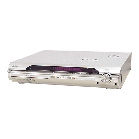
HCD-DX375 is the amplifier, DVD/CD and tuner
section in DAV-DX375.
This system incorporates with Dolby*
adaptive matrix surround decoder and the DTS*
System.
*1 Manufactured under license from Dolby Laboratories.
"Dolby," "Pro Logic," and the double-D symbol are trademarks of
Dolby Laboratories.
*2 Manufactured under license from Digital Theater Systems, Inc.
"DTS" and "DTS Digital Surround" are trademarks of Digital
Theater Systems, Inc.
AUDIO POWER SPECIFICATIONS
POWER OUTPUT AND
TOTAL HARMONIC
DISTORTION
(FTC Output Power):
FL/FR/SL/SR/C: 84 W/ch
3 ohm at 170 - 20,000 Hz,
0.7 % THD
SW: 160 W 1.5 ohm at 40 -
170 Hz, 0.7 % THD
Amplifier section
Surround mode (reference) RMS output power, 10 %
THD
Front: 143 W + 143 W
(with SS-TS52)
Center*: 143 W
(with SS-CT51)
Surround*: 143 W + 143
W
(with SS-TS51)
Subwoofer*: 285 W
(with SS-WS52B)
* Depending on the sound field settings and the source,
there may be no sound output.
Sony Corporation
9-887-160-02
Home Audio Division
2006D16-1
Published by Sony Techno Create Corporation
© 2006.04
HCD-DX375
1
Digital and Dolby Pro Logic (II)
2
Digital Surround
SPECIFICATIONS
Inputs
TV, VCR (AUDIO IN)
AUDIO IN
Outputs (Analog)
Phones
Super Audio CD/DVD system
Laser
Signal format system
Harmonic distortion
Tuner section
System
FM tuner section
Tuning range
Antenna (aerial)
Antenna (aerial) terminals 75 ohms, unbalanced
Intermediate frequency
Model Name Using Similar Mechanism
Mechanism Type
Optical Pick-up Name
AM tuner section
Sensitivity: 450/250 mV
Tuning range
Sensitivity: 250/125 mV
Accepts low-and high-
impedance headphones.
Antenna (aerial)
Intermediate frequency
Semiconductor laser
Video section
(Super Audio CD/DVD:
Outputs
λ = 650 nm)
(CD: λ = 790 nm)
Emission duration:
continuous
NTSC
Less than 0.03 %
PLL quartz-locked digital
synthesizer system
87.5 – 108.0 MHz
(100 kHz step)
FM wire antenna (aerial)
10.7 MHz
SUPER AUDIO CD/DVD RECEIVER
US Model
HCD-DX255
CDM81C-DVBU101
KHM-310CAB
530 – 1,710 kHz (with the
interval set at 10 kHz)
531 – 1,710 kHz (with the
interval set at 9 kHz)
AM loop antenna (aerial)
450 kHz
VIDEO: 1 Vp-p 75 ohms
S VIDEO:
Y: 1 Vp-p 75 ohms
C: 0.286 Vp-p 75 ohms
COMPONENT:
Y: 1 Vp-p 75 ohms
P
/C
, P
/C
: 0.7 Vp-p
B
B
R
R
75 ohms
HDMI OUT:
Type A (19 pin)
— Continued on next page —
Advertisement
Table of Contents

Related Manuals for Sony HCD-DX375


Summary of Contents for Sony HCD-DX375
-
Page 1: Service Manual
HCD-DX375 SERVICE MANUAL US Model Ver. 1.1 2006.04 HCD-DX375 is the amplifier, DVD/CD and tuner section in DAV-DX375. This system incorporates with Dolby* Digital and Dolby Pro Logic (II) Model Name Using Similar Mechanism HCD-DX255 adaptive matrix surround decoder and the DTS*... -
Page 2: Leakage Test
COMPONENTS IDENTIFIED BY MARK 0 OR DOTTED LINE WITH MARK 0 ON THE SCHEMATIC DIAGRAMS AND IN THE PARTS LIST ARE CRITICAL TO SAFE OPERATION. REPLACE THESE COMPONENTS WITH SONY PARTS WHOSE PART NUMBERS APPEAR AS SHOWN IN THIS MANUAL OR IN SUPPLEMENTS PUBLISHED BY SONY. -
Page 3: Table Of Contents
HCD-DX375 TABLE OF CONTENTS SERVICING NOTE 6-8. Schematic Diagram – DMB12 Board (1/7) – ....41 ........... 4 6-9. Schematic Diagram – DMB12 Board (2/7) – ....42 6-10. Schematic Diagram – DMB12 Board (3/7) – ....43 GENERAL ..............11 6-11. -
Page 4: Servicing Note
Although this is not a seconds again. malfunction and for Sony service use only, 2. The message “UNLOCKED” is displayed and the tray is normal system operation will not be possible. unlocked. - Page 5 HCD-DX375 HOW TO OPEN THE DISC TABLE WHEN POWER SWITCH TURNS OFF tweezers Insert tip of tweezers through the hole gear of bottom plate, and roate the gear in the counter-clockwise direction. DVD lid tape Attach an adhesive tape on the DVD LID and draw it out.
- Page 6 HCD-DX375 Fix the capacitors with adhesive agent as follows Fixing the capacitors with adhesive agent is required by the safety regulation. Be sure to fix the capacitors with adhesive agent when part or circuit board is replaced. POWER BOARD Precaution when replacing the CAP Please apply the adhesive agent to the BUTTON BASE (PLAY) when replacing the CAP (PLAY) or CAP (FUNC) or CAP (AMS).
- Page 7 HCD-DX375 PRECAUTION WHEN INSTALLING A NEW OP UNIT / PRECAUTION BEFORE UNSOLDERING THE STATIC ELECTRICITY PREVENTION SOLDER BRIDGE When installing a new OP unit, be sure to connect the flexible printed circuit board first of all before removing the static electricity prevention solder bridge by unsoldering.
- Page 8 HCD-DX375 • DMB12 board service position DMB12 board Remove the DMB12 board once. Then create the service position. DMB12 board...
- Page 9 HCD-DX375 • POWER board service position DMB12 board Remove the DMB12 board and POWER board once. Then create the service position. POWER board Connect the flexible cable and Front panel assy harnesses from the front panel assy. Inshuration sheet DMB12 board...
- Page 10 HCD-DX375 • MAIN board service position DMB12 board, bracket (HDMI) Remove the three connectors of D.C.fan the SPEAKER board. MAIN board SPEAKER board Remove the DMB12 board , bracket (HDMI), D.C.fan and the MAIN board once. Then create the service position.
-
Page 11: General
HCD-DX375 SECTION 2 GENERAL This section is extracted from instruction manual. Front panel A "/1 (on/standby) (30) G PHONES jack (30) H VOLUME control (30) B Front panel display (93) I AUDIO IN/A.CAL MIC jack (19, 32) C A (open/close) (30) - Page 12 HCD-DX375 Front panel display About the indications in the front panel display A Lights up when the HDMI OUT jack is H Lights up during MULTI channel correctly connected to HDCP (high- playback. (Super Audio CD only) (49) bandwidth digital content protection)
-
Page 13: Remote Control
After pressing the TV button w;, you can control the menu on a Sony TV. On the menu screen, DISPLAY button ea doubles as the MENU button, and the AMP MENU button 7 double as the TOOLS button. -
Page 14: Disassembly
HCD-DX375 SECTION 3 DISASSEMBLY 3-1. DISASSEMBLY FLOW • This set can be disassembled in the order shown below. • The dotted square with arrow ( ) prompts you to move to the next job when all of the works within the dotted square ( ) are completed. -
Page 15: Case, Front Panel Assy
HCD-DX375 Note: Follow the disassembly procedure in the numerical order given. 3-2. CASE, FRONT PANEL ASSY 4 two screws (CASE3 TP2) 6 five screws (+BVTP 3 × 8) 7 case 9 w ire (flat type) 5 two screws 23core (CN501) -
Page 16: Fl Board, Sw Board
HCD-DX375 3-3. FL BOARD, SW BOARD When reassembling, route the harness and flexible cable as shown in the illustration. 9 wire (flat type) qg cap (power) 23core (CN801) 7 connector (CN811) qf button base (power) 8 connector (CN805) qd SW board... -
Page 17: Dmb12 Board
HCD-DX375 3-5. DMB12 BOARD 4 connector (CN601) 5 wire (flat type) 5core (CN4302) 6 wire (flat type) 11core (CN4301) 7 wire (flat type) 9core (CN4501) 8 seven screws (+BV 3) 3 wire (flat type) 24core (CN101) q; DMB12 board 2 connector (CN201) -
Page 18: I/O Board, Tuner
HCD-DX375 3-6. I/O BOARD, TUNER 7 wire (flat type) 5core(CN202) 8 wire (flat type)11core(CN201) 5 wire (flat type) 3 tuner 9core(CN203) qa I/O board 4 connector 1 two screws (CN312) (+BVTT 3 × 6) 6 wire (flat type) 2 wire (flat type) 15core(CN311) q;... -
Page 19: Main Board
HCD-DX375 3-8. MAIN BOARD 4 wire (flat type) 9core (CN701) 6 connector (CN303) 5 connector (CN303) 7 connector (CN302) 3 wire (flat type) 15core (CN601) 8 connector (CN301) 2 wire (flat type) 21core (CN622) 1 wire (flat type) 23core (CN501) -
Page 20: Power Board
HCD-DX375 3-9. POWER BOARD 6 five screws (+PWH 3 × 8) 7 POWER board 4 two screws (+BV 3) 5 shield (H/L) 1 connector (CN506) 2 connector (CN3002) 3 connector (CN901) When re-assembling, leave 30 mm between harnesses A and B for safety. -
Page 21: Dvd Mechanism Deck (Cdm81C-Dvbu101)
HCD-DX375 3-10. DVD MECHANISM DECK (CDM81C-DVBU101) 3 four screws (+BV 3) MD cover 2 Remove the harness and flexible cable. harness flexible cable 1 wire (flat type) 21core (CN622) 5 four screws (+BVTP 3 × 10) 6 DVD mechanism deck... -
Page 22: Tray
HCD-DX375 3-11. TRAY 2 two screws (+BTTP 2.6) 3 bracket 1 two screws (+BTTP 2.6) 5 tray 3-12. MOTOR BOARD M761 (LD/ST MOTOR), M762 (BU U/D MOTOR) 1 screw (+BTTP 2.6) 3 screw (+BTTP 2.6) 2 bracket 4 MOTOR board 5 Remove soldering from the two points. -
Page 23: Base Unit (Dvbu101)
HCD-DX375 3-13. BASE UNIT (DVBU101) 1 two floating screws (+PTPWH2.6) 3 base unit (DVBU101) 2 floating screw (+PTPWH2.6) 3-14. OPTICAL PICK-UP (KHM-310CAB) qa insulator 7 insulator screw 3 insulator screw qs insulator 9 insulator 8 insulator screw 4 insulator screw... -
Page 24: Gear (Sub Tray 1), Gear (Sub Tray 2)
HCD-DX375 3-15. GEAR (SUB TRAY 1), GEAR (SUB TRAY 2) PRECAUTION DURING GEAR (SUB TRAY 1/2) INSTALLATION 1 five screws (+PTPWH 2.6 × 8) Align the marks of the gears as shown in the illustration. 4 three gears (sub tray 1) -
Page 25: Stocker Section
HCD-DX375 3-17. STOCKER SECTION 2 stocker section 1 Rotate the gear (SS3) in the direction of the arrow. 3-18. CAM (STOCKER) PRECAUTION DURING CAM (STOCKER) INSTALLATION Before installing the cams (stocker), fix the gear (stocker 3) in the manner so that the hole of the gear (stocker 3) should be... -
Page 26: Gear (Stocker 3)
HCD-DX375 3-19. GEAR (STOCKER 3) PRECAUTION DURING GEAR (STOCKER 3) INSTALLATION 1 screw (+PTPWH 2.6 × 8) Be sure to align the rib of the gear (stocker 3) with the groove of the rotary encoder. 2 gear (stocker 3) groove... -
Page 27: Gear (Bu1)
HCD-DX375 3-21. GEAR (BU1) 1 belt (sub tray) PRECAUTION DURING GEAR (BU1) INSTALLATION 4 screw 2 screw Before re-assembling, slide the cam (BU) in the direction of (+PTPWH 2.6 × 8) (+PTPWH 2.6 × 8) the arrow. Assemble the gear (BU1) in such a manner that the groove 3 pulley (BU) of the cam (BU) is aligned with the rib of the gear (BU1). -
Page 28: Test Mode
HCD-DX375 Ver. 1.1 SECTION 4 TEST MODE 3. Disc Tray Lock Note 1: Regarding the notification symbol “R” The disc tray lock function for the antitheft of an demonstration Because the number of the operating buttons of this product disc in the store is equipped. - Page 29 HCD-DX375 Ver. 1.1 8-4. MIRROR TIME ADJUSTMENT DVD SECTION To enter Mirror Time Adjustment, press 5 “R” button on the remote [TEST DISC LIST] commander. The screen will appear as below. Be sure to use the DVD disc that matches the signal standards of MIRR time Adjust Menu your region.
- Page 30 HCD-DX375 (3) Select “5. MIRR time Adjust”. (14) Confirm the same values are displayed. If it is not same, return to step 7. Drive Manual Operation MIRR time Adjust Menu 1. Servo Control 2. Track/Layer Jump 1. CD MIRR time Check: 3.
- Page 31 HCD-DX375 Ver. 1.1 8-5. EXECUTING IOP MEASUREMENT (5) Wait until a hexadecimal number appear. Manual Adjust In order to execute mirror time adjustment, the following standard procedures must be followed. 1. Track Balance Adjust: 2. Track Gain Adjust: and A buttons (1) In standby mode, while pressing the 3.
-
Page 32: Electrical Adjustment
HCD-DX375 SECTION 5 ELECTRICAL ADJUSTMENT Checking Location: DMB12 board (Side A) DVD SECTION DMB12 BOARD (SIDE A) When the base unit is replaced, perform the adjustment and the measurement as shown below in this order. 1) MIRROR TIME ADJUSTMENT (See page 29) -
Page 33: Diagrams
HCD-DX375 SECTION 6 DIAGRAMS • Circuit Boards Location THIS NOTE IS COMMON FOR PRINTED WIRING BOARDS AND SCHEMATIC DIAGRAMS. (In addition to this, the necessary note is printed in each block.) For Schematic Diagrams. For Printed Wiring Boards. Note: Note: •... -
Page 34: Block Diagram - Rf Section
HCD-DX375 6-1. BLOCK DIAGRAM – RF SECTION – CN105 RFMON V2REFO DVDRFIP V2REFO TO DIAG JIG • Signal Path : CD PLAY DVDA : DVD PLAY DVDB DETECTOR : SACD PLAY DVDC DVDD VIDEO SECTION 8 NA (Page 37) IC621... -
Page 35: Block Diagram - Amp Section
HCD-DX375 6-2. BLOCK DIAGRAM – AMP SECTION – IC352 IC101 (3/3) AUDIO INPUT SELECTOR DVD SYSTEM PROCESSOR 220 SPDATA IC353 11 X3 IC401 IC4601 15 X2 A/D CONVERTER L-CH 14 X1 – 1 LIN DOUT J401 – AMP LRCKO AUDIO... -
Page 36: Block Diagram - Audio Section
HCD-DX375 6-3. BLOCK DIAGRAM – AUDIO SECTION – IC3001 COMPARATOR J402 – PHONES – PLUG DET2 Q450,451 HPMUTE Q3081 Q460,461 MUTE SW IC3500 MUTE S-MASTER DIGITAL AMP • Signal Path PWMB OUTB : AUDIO PWMA OUTA RESET IC3030 S-MASTER PROCESSOR... -
Page 37: Block Diagram - Video Section
HCD-DX375 6-4. BLOCK DIAGRAM – VIDEO SECTION – AMP LRCKO,AMP MCKO,AMPBCKO AUDIO SECTION AMP SECTION (Page 35) (Page 36) AMPDO,AMPD2,AMPD3 AUDIO SECTION (Page 36) SPDIF TX2P SPDIF TMDS DATA2 + ALRCK ALRCK TX2N TMDS DATA2 - ABCK ABCK TMDS DATA1 +... -
Page 38: Block Diagram - Power Section
HCD-DX375 6-5. BLOCK DIAGRAM – POWER SECTION – POWER Thermistor F901 T901 D901 TRANSFORMER(MAIN) AC IN LINE FILTER D931 IC901 D905 +31.5V Q901 T801 POWER VOLTAGE DC/DC PROTECTION CONTROLLER IC931 CONVERTER VOLTAGE DETECT PC901 TO FLUORESCENT PHOTO INDICATOR TUBE D801,802... -
Page 39: Printed Wiring Board - Dmb12 Board (Side A)
HCD-DX375 6-6. PRINTED WIRING BOARD – DMB12 BOARD (SIDE A) – See page 33 for Circuit Boards Location. :Uses unleaded solder. New part of EEP ROM (IC103, IC706) on the DMB12 board cannot be used. Therefore, if the mounted MAIN board (A-1148-813-A) is... -
Page 40: Printed Wiring Board - Dmb12 Board (Side B)
HCD-DX375 6-7. PRINTED WIRING BOARD – DMB12 BOARD (SIDE B) – See page 33 for Circuit Boards Location. :Uses unleaded solder. • Semiconductor Location Ref. No. Location R754 IC105 IC705 IC107 IC150 R756 IC111 IC150 IC702 IC703 IC705 IC706 IC707... -
Page 41: Schematic Diagram - Dmb12 Board (1/7)
HCD-DX375 6-8. SCHEMATIC DIAGRAM – DMB12 BOARD (1/7) – See page 66 for IC Block Diagram. CN4301 R4701 JL4703 CN601 JL4704 FL601 FB604 FB602 JL611 JL612 JL4705 JL613 JL614 FL603 C602 R4702 JL4706 FB603 FB606 JL609 JL610 JL4707 C603 JL4708... -
Page 42: Schematic Diagram - Dmb12 Board (2/7)
HCD-DX375 Ver. 1.1 New part of EEP ROM (IC103, IC706) on the DMB12 board cannot be used. 6-9. SCHEMATIC DIAGRAM – DMB12 BOARD (2/7) – Therefore, if the mounted MAIN board (A-1148-813-A) is replaced, exchange new EEP ROM (IC103, IC706) with that used before the replacement. -
Page 43: Schematic Diagram - Dmb12 Board (3/7)
HCD-DX375 6-10. SCHEMATIC DIAGRAM – DMB12 BOARD (3/7) – See page 65 for Waveforms. See page 73 for IC Pin Function Description. R1120 R1121 R1122 R1186 R1169 R1123 R1124 FB112 R189 R190 R192 R195 R197 R1102 R146 C161 C163 R1125... -
Page 44: Schematic Diagram - Dmb12 Board (4/7)
HCD-DX375 6-11. SCHEMATIC DIAGRAM – DMB12 BOARD (4/7) – See page 67 for IC Block Diagram. IC104 EDS6416AHT A-75-E C197 C181 RB108 C180 RB106 C191 RB107 1/32W C179 RB105 C190 1/32W FB108 R1150 3.3k 1/10W R1151 3.3k 1/10W R1152 3.3k... -
Page 45: Schematic Diagram - Dmb12 Board (5/7)
HCD-DX375 6-12. SCHEMATIC DIAGRAM – DMB12 BOARD (5/7) – R230 R231 R232 R223 R225 100k 1/10W 100k 1/10W R234 1/10W 1/10W 1/10W 0.5% 0.5% 0.5% 0.5% 0.5% C209 0.033 C211 C212 CL206 0.033 C215 0.01 R221 0.01 C233 0.0047 R220 1/10W 0.5%... -
Page 46: Schematic Diagram - Dmb12 Board (6/7)
HCD-DX375 New part of EEP ROM (IC103, IC706) on the DMB12 board cannot be used. 6-13. SCHEMATIC DIAGRAM – DMB12 BOARD (6/7) – See page 66, 67 for IC Block Diagrams. Therefore, if the mounted MAIN board (A-1148-813-A, etc.) is replaced, exchange new EEP ROM (IC103, IC706) with that used before the replacement. -
Page 47: Schematic Diagram - Dmb12 Board (7/7)
HCD-DX375 6-14. SCHEMATIC DIAGRAM – DMB12 BOARD (7/7) – See page 65 for Waveform. R763 R762 R772 R783 R784 C732 0.01 CL742 Q702 2SK1399-T1B CL743 Q701 2SK1399-T1B CL744 CL745 CL755 R781 R785 R786 R782 R766 4.7k IC708 R767 MB95F108ASPFV- GE1-H0601... -
Page 48: Printed Wiring Board - Main Board (Side A)
HCD-DX375 6-15. PRINTED WIRING BOARD – MAIN BOARD (SIDE A) – See page 33 for Circuit Boards Location. :Uses unleaded solder. DMB12 BOARD CN109 for WRITER JIG (Page 39) • Semiconductor Location IC3050 Ref. No. Location IC501 D-10 IC502 C-13... -
Page 49: Printed Wiring Board - Main Board (Side B)
HCD-DX375 6-16. PRINTED WIRING BOARD – MAIN BOARD (SIDE B) – See page 33 for Circuit Boards Location. :Uses unleaded solder. POWER BOARD POWER BOARD JACK BOARD CN904 CN902 CN403 SOFT JIG (Page 63) (Page 63) (Page 58) (CHASSIS) (CHASSIS) -
Page 50: Schematic Diagram - Main Board (1/6)
HCD-DX375 Ver. 1.1 6-17. SCHEMATIC DIAGRAM – MAIN BOARD (1/6) – See page 68 for IC Block Diagrams. R3060 R3059 EB3001 TERMINAL BOARD C3035 C3034 R3062 TP3031 R3063 R3031 R3064 TP3003 R3065 TP3004 R3066 ICT3063 R3067 R3032 R3068 R3069 TP3032... -
Page 51: Schematic Diagram - Main Board (2/6)
HCD-DX375 Ver. 1.1 6-18. SCHEMATIC DIAGRAM – MAIN BOARD (2/6) – See page 68 for IC Block Diagrams. R3501 R3502 C3406 0.033 ICT3010 C3403 ICT3011 C3413 ICT3060 R3061 C3551 1 50V R3403 TP3410 C3412 ICT3061 R3404 R3551 100k ICT3050 R3407... -
Page 52: Schematic Diagram - Main Board (3/6)
HCD-DX375 Ver. 1.1 6-19. SCHEMATIC DIAGRAM – MAIN BOARD (3/6) – See page 65 for Waveform. See page 68 for IC Block Diagrams. R3055 C3015 C3014 R3011 R3050 ICT3003 Q3081 R3012 ICT3004 RT1P141C TP3011 R3151 R3013 TP3012 C3013 R3091 C3083... -
Page 53: Schematic Diagram - Main Board (4/6)
HCD-DX375 Ver. 1.1 6-20. SCHEMATIC DIAGRAM – MAIN BOARD (4/6) – See page 68 for IC Block Diagrams. MAIN C3206 0.033 ICT3027 C3203 Q3252 ICT3028 2SA1235TP-1EF C3213 Q3202 2SA1235TP-1EF R3203 TP3210 C3212 R3204 C3220 0.0022 ICT3082 R3207 C3215 C3272 C3219 0.0022... -
Page 54: Schematic Diagram - Main Board (5/6)
HCD-DX375 6-21. SCHEMATIC DIAGRAM – MAIN BOARD (5/6) – See page 65 for Waveform. See page 70 for IC Pin Function Description. R554 R534 CN601 R540 C518 TP605 R604 R501 TP606 R605 ICT538 R503 TP607 R606 TP608 R607 C504 0.01... -
Page 55: Schematic Diagram - Main Board (6/6)
HCD-DX375 6-22. SCHEMATIC DIAGRAM – MAIN BOARD (6/6) – IC622 BH2210FV-E2 RB626 RB630 TP646 TP645 TP644 TP643 RB629 R623 RB625 FB504 C625 ICT550 R634 C534 FB506 TP537 C532 EB505 FL502 TERMINAL BOARD FB501 FB507 GROUND R633 TP536 CN622 C622 C535... -
Page 56: Printed Wiring Board - I/O Board
HCD-DX375 6-23. PRINTED WIRING BOARD – I/O BOARD – See page 33 for Circuit Boards Location. :Uses unleaded solder. • Semiconductor Location COMPONENT Ref. No. Location VIDEO OUT IC201 VIDEO IC352 IC353 MONITOR OUT IC360 S VIDEO Q353 (DVD ONLY) -
Page 57: Schematic Diagram - I/O Board
HCD-DX375 6-24. SCHEMATIC DIAGRAM – I/O BOARD – See page 65 for Waveforms. See page 69 for IC Block Diagrams. CN203 CN312 AMP-S 5P C345 R381 R382 TP353 C349 R356 TP354 4.7k TP355 C346 22 25V TP356 TP357 R344 C350... -
Page 58: Printed Wiring Boards - Panel Section
HCD-DX375 6-25. PRINTED WIRING BOARDS – PANEL SECTION – See page 33 for Circuit Boards Location. :Uses unleaded solder. MAIN BOARD CN501 (Page 48) IC801 IC802 I/O BOARD CN312 (Page 56) FUNCTION > VOLUME – IC803 DISC 5 DISC 4... -
Page 59: Schematic Diagram - Panel Section
HCD-DX375 6-26. SCHEMATIC DIAGRAM – PANEL SECTION – See page 67, 69 for IC Block Diagrams. Q814 Q815 RT1P141C-TP-1 RT1P141C-TP-1 R835 R834 R833 R836 D812 D813 SML79423C-TP15 SML79423C-TP15 R852 R851 R827 R828 R829 R830 R841 2.2k Q816 2.2k 4.7k Q813... -
Page 60: Printed Wiring Board - Speaker Board
HCD-DX375 6-27. PRINTED WIRING BOARD – SPEAKER BOARD – 6-28. SCHEMATIC DIAGRAM – SPEAKER BOARD – See page 33 for Circuit Boards Location. :Uses unleaded solder. EP301 EARTH PLATE SPEAKER (CHASSIS) TB301 DICS 4P FRONT R FRONT L CENTER WOOFER... -
Page 61: Printed Wiring Boards - Cd Mechanism Section
HCD-DX375 6-29. PRINTED WIRING BOARDS – CD MECHANISM SECTION – See page 33 for Circuit Boards Location. :Uses unleaded solder. • Semiconductor MOTOR BOARD Location Ref. No. Location D701 D711 IC701 IC711 IC751 Q751 SENSOR BOARD M761 M762 1-861-240- (12) -
Page 62: Schematic Diagram - Cd Mechanism Section
HCD-DX375 6-30. SCHEMATIC DIAGRAM – CD MECHANISM SECTION – • See page 69 for IC Block Diagrams. (6/6) CN622 (Page 55) HCD-DX375... -
Page 63: Printed Wiring Board - Power Board
HCD-DX375 6-31. PRINTED WIRING BOARD – POWER BOARD – See page 33 for Circuit Boards Location. :Uses unleaded solder. • Semiconductor Location Ref. No. Location D901 B-11 IC901 D905 D906 D907 D908 D909 D910 D913 D914 D915 D921 D922 PC902... -
Page 64: Schematic Diagram - Power Board
HCD-DX375 6-32. SCHEMATIC DIAGRAM – POWER BOARD – (CHASSIS) D931 FCU20UC20 C938 EB905 330p 250V CN902 TP903 WIRE 3P CN901 TH901 T901 FH901 FH902 C963 THERMISTOR HOLDER HOLDER D901 C930 MAIN TRANS L931 TP901 R931 R940 R937 FUSE FUSE 0.0022... - Page 65 HCD-DX375 • Waveforms – DMB12 Board – – I/O Board – IC101 6 (DVDRFIP) IC201 wd (CVBS) IC201 w; (CYOUT) 2.5 Vp-p 2.0 Vp-p 800 mVp-p 1 V/DIV, 20 µ s/DIV 1 V/DIV, 20 µ s/DIV 200 mV/DIV, 100 ns/DIV...
-
Page 66: Ic Block Diagrams
HCD-DX375 • IC Block Diagrams – DMB12 Board – IC706 BR24L16F-WE2 1 A0 16 K bit EEPROM ARRAY 11 bit 8 bit 2 A1 ADDRESS SLAVE WORD DATA 11 bit DECODER ADDRESS REGISTER REGISTER START STOP 3 A2 CONTROL CIRCUIT... - Page 67 HCD-DX375 – DMB12 Board – IC702 TK11118CSCL-G IC150, IC705 SN74LVC1G08DCKR OVER HEAT & OVER CURRENT PROTECTION CONTROL CIRCUIT BANDGAP REFERENCE – FL Board – IC802 PT6315 Grid driver Multiplexed driver SEG19/GRID10 Command decoder LED1 SEG18/GRID11 LED2 Display memory LED3 SEG17/GRID12...
- Page 68 HCD-DX375 – MAIN Board – IC3100, IC3150, IC3200, IC3250, IC3300, IC3400, IC3500 CXD9883M BST_A PVDD_A Over Current Fault GVDD_A PVDD_A /OTW PVDD_A VREG Gate Drive /HIZ_HS_A PGND /HIZ_LS_A Stuck Detect /RESET PGND Protection Logic Timing PWM_A PGND Control /OCH_A Programmable...
-
Page 69: Relay Board
HCD-DX375 – I/O Board – IC201 MM1623BFBE IC352 MC14052BDR2 S-DC OUT 28 VCC2 S1/S2 27 S-DC OUT 150kΩ 75Ω VCC1 BIAS 6.75MHz DRIVER LOW-PASS C IN 26 C OUT FILTER MUTE 1 25 S1 CLAMP –6dB 24 S2 CVBS IN 75Ω... - Page 70 HCD-DX375 Ver. 1.1 • IC Pin Function Description MAIN BOARD IC501 M30622MEP-A61FPU0 (SYSTEM CONTROLLER) Pin No. Pin Name Description DAMP_SCDT/ DAMP processor and Diat data output DIAT_SDATA DAMP_SHIFT/ DAMP processor and Diat clock output DIAT_SCLK DSP_INTR DSP interrupt (not used)
- Page 71 HCD-DX375 Ver. 1.1 Pin No. Pin Name Description DRIVE_OCP (DIAG) DAMP driver shut down OVERFLOW1 DAMP processor F/C/S over flow detect OVERFLOW2 DAMP processor SW over flow detect Flash write CE (not used) DAMP LATCH1 DAMP processor latch1 DAMP LATCH2...
- Page 72 HCD-DX375 Pin No. Pin Name Description IO_DO I/O expander IC data input IO_CLK I/O expander IC clock output MONO/ST_DET Front jack MONO or STEREO detect A.CAL MIC LEVEL/ MIC level detect for auto calibration A_SEL2 DESTINATION Destination select input MODEL...
- Page 73 HCD-DX375 DMB12 BOARD IC101 CXD9804R (CD/DVD RF AMP, FOCUS/TRACKING ERR AMP, DVD SYSTEM PROCESSOR, DIGITAL SERVO PROCESSOR) Pin No. Pin Name Description AGND — Ground terminal DVDA AC coupled input path A DVDB AC coupled input path B DVDC AC coupled input path C...
- Page 74 HCD-DX375 Pin No. Pin Name Description Mute signal control output CKSW — Not used OCSW — Not used EEWP WF signal output to EEPROM (IC103) DVDD18 — Power supply (+1.8V from IC110) 53 to 59 HA 2 to 8 Address bus 2 to 8 output to FLASH ROM (IC102)
- Page 75 HCD-DX375 Pin No. Pin Name Description Data bus 7 from SD-RAM (IC104) DVSS — Ground terminal 117, 118 RD 6, 5 Data bus 6, 5 from SD-RAM (IC104) DVSS — Ground terminal 120, 121 RD 4, 3 Data bus 4, 3 from SD-RAM (IC104) DVDD18 —...
- Page 76 HCD-DX375 Pin No. Pin Name Description MUTE MUTE signal output to Motor Driver (IC201) MUTE123 MUTE123 signal output to Motor Driver (IC201) REW signal output to Motor Driver (IC201) FWD signal output to Motor Driver (IC201) ADSD0 Not used XDACS...
- Page 77 HCD-DX375 Pin No. Pin Name Description PLLVSS — Ground terminal IDAC — Not used PLLVDD3 — Power supply (RF+3.3V) LPFON Negative output of loop filter amplifier LPFIP Positive input of loop filter amplifier LPFIN Negative input of loop filter amplifier...
-
Page 78: Exploded Views
HCD-DX375 SECTION 7 EXPLODED VIEWS NOTE: • -XX and -X mean standardized parts, so they • The mechanical parts with no reference The components identified by mark 0 or may have some difference from the original number in the exploded views are not supplied. -
Page 79: Front Panel Section
HCD-DX375 7-2. FRONT PANEL SECTION supplied supplied supplied supplied including S800 Ref. No. Part No. Description Remark Ref. No. Part No. Description Remark 2-654-836-01 KNOB (VOL) 2-653-091-01 BUTTON (DISC) 2-654-835-01 RING (VOL) 2-653-094-01 INDICATOR (DISC) 2-653-097-01 ORNAMENT (RIGHT) A-1148-824-A JACK BOARD, COMPLETE... -
Page 80: Chassis Section
HCD-DX375 7-3. CHASSIS SECTION supplied not supplied supplied supplied F901 supplied DVD mechanism deck section supplied not supplied Ref. No. Part No. Description Remark Ref. No. Part No. Description Remark 3-077-331-21 +BV3 (3-CR) 4-232-478-41 FOOT 1-828-319-11 WIRE (FLAT TYPE) (11 CORE) -
Page 81: Dvd Mechanism Deck Section-1 (Cdm81C-Dvbu101)
HCD-DX375 7-4. DVD MECHANISM DECK SECTION-1 (CDM81C-DVBU101) not supplied Ref. No. Part No. Description Remark Ref. No. Part No. Description Remark 4-251-849-01 LEVER (SW2) 4-251-829-02 TRAY (SUB) 4-251-991-01 SPRING (SW2), TORSION 4-251-860-01 LEVER (LOCK) 4-985-672-01 SCREW (+PTPWH M2.6), FLOATING 4-251-867-01 SPRING (LOCK), TORSION... -
Page 82: Dvd Mechanism Deck Section-2 (Cdm81C-Dvbu101)
HCD-DX375 7-5. DVD MECHANISM DECK SECTION-2 (CDM81C-DVBU101) not supplied not supplied M761 M762 S771 not supplied not supplied Ref. No. Part No. Description Remark Ref. No. Part No. Description Remark 4-251-870-01 BELT (BU) 4-251-854-01 GEAR (BU1) 4-251-869-01 BELT (MAIN TRAY) -
Page 83: Dvd Mechanism Deck Section-3 (Cdm81C-Dvbu101)
HCD-DX375 7-6. DVD MECHANISM DECK SECTION-3 (CDM81C-DVBU101) not supplied CDM81C-DVBU101 not supplied not supplied S781 not supplied Ref. No. Part No. Description Remark Ref. No. Part No. Description Remark 4-985-672-01 SCREW (+PTPWH M2.6), FLOATING 4-251-823-01 CHASSIS (CDM81) 4-251-873-01 SPRING (MODE), COMPRESSION... -
Page 84: Base Unit (Dvbu101)
HCD-DX375 7-7. BASE UNIT (DVBU101) Ref. No. Part No. Description Remark Ref. No. Part No. Description Remark X-4956-097-1 HOLDER (310) ASSY 3-087-599-01 INSULATOR SCREW 0 302 8-820-291-02 OPTICAL PICK-UP (KHM-310CAB/C2RP) 7-685-534-19 SCREW +BTP 2.6X8 TYPE2 N-S 2-634-618-01 INSULATOR... -
Page 85: Electrical Parts List
HCD-DX375 SECTION 8 DMB12 ELECTRICAL PARTS LIST NOTE: • Due to standardization, replacements in the • COILS When indicating parts by reference number, parts list may be different from the parts uH: H please include the board name. specified in the diagrams or the components •... - Page 86 HCD-DX375 Ver. 1.1 DMB12 Ref. No. Part No. Description Remark Ref. No. Part No. Description Remark C218 1-124-779-00 ELECT CHIP 10uF < CONNECTOR > C219 1-162-970-11 CERAMIC CHIP 0.01uF CN101 1-815-763-32 CONNECTOR, FFC/FPC 24P C220 1-124-779-00 ELECT CHIP 10uF * CN105...
- Page 87 HCD-DX375 DMB12 Ref. No. Part No. Description Remark Ref. No. Part No. Description Remark < COIL > R154 1-216-864-11 SHORT CHIP L3601 1-469-555-21 INDUCTOR 10uH R155 1-216-864-11 SHORT CHIP L4602 1-469-555-21 INDUCTOR 10uH R156 1-216-809-11 METAL CHIP 1/10W R159 1-216-805-11 METAL CHIP 1/10W <...
- Page 88 HCD-DX375 DMB12 Ref. No. Part No. Description Remark Ref. No. Part No. Description Remark R703 1-216-864-11 SHORT CHIP R704 1-216-864-11 SHORT CHIP R1101 1-218-855-11 METAL CHIP 2.2K 0.5% 1/10W R705 1-216-829-11 METAL CHIP 4.7K 1/10W R1102 1-218-827-11 METAL CHIP 0.5%...
- Page 89 HCD-DX375 DMB12 Ref. No. Part No. Description Remark Ref. No. Part No. Description Remark R4505 1-216-864-11 SHORT CHIP A-1148-821-A FL BOARD, COMPLETE R4506 1-216-864-11 SHORT CHIP ****************** R4507 1-216-864-11 SHORT CHIP < CAPACITOR > R4510 1-469-311-22 BEAD, FERRITE (CHIP) (1608)
- Page 90 HCD-DX375 Ref. No. Part No. Description Remark Ref. No. Part No. Description Remark < SHORT > C228 1-126-933-11 ELECT 100uF C234 1-126-382-11 ELECT 100uF JR807 1-216-296-11 SHORT CHIP C235 1-104-662-91 ELECT 22uF C236 1-104-662-91 ELECT 22uF < COIL > C239 1-164-156-11 CERAMIC CHIP 0.1uF...
- Page 91 HCD-DX375 JACK Ref. No. Part No. Description Remark Ref. No. Part No. Description Remark < TRANSISTOR > R378 1-216-841-11 METAL CHIP 1/10W Q353 8-729-027-52 TRANSISTOR RT1N241C-TP-1 R381 1-216-841-11 METAL CHIP 1/10W Q354 8-729-027-52 TRANSISTOR RT1N241C-TP-1 R382 1-216-841-11 METAL CHIP 1/10W...
- Page 92 HCD-DX375 JACK Ref. No. Part No. Description Remark Ref. No. Part No. Description Remark < IC > R463 1-216-829-11 METAL CHIP 4.7K 1/10W R464 1-216-829-11 METAL CHIP 4.7K 1/10W IC401 8-759-100-96 IC NJM4558M-TE2 R470 1-216-825-11 METAL CHIP 2.2K 1/10W IC402...
- Page 93 HCD-DX375 MAIN Ref. No. Part No. Description Remark Ref. No. Part No. Description Remark R832 1-216-815-11 METAL CHIP 1/10W C525 1-107-826-11 CERAMIC CHIP 0.1uF R833 1-216-817-11 METAL CHIP 1/10W C526 1-104-658-91 ELECT 100uF C527 1-104-656-11 ELECT 2200uF 6.3V R834 1-216-815-11 METAL CHIP...
- Page 94 HCD-DX375 MAIN Ref. No. Part No. Description Remark Ref. No. Part No. Description Remark C3058 1-162-910-11 CERAMIC CHIP 0.25PF 50V C3166 1-112-831-11 ELECT 2200uF C3167 1-162-966-11 CERAMIC CHIP 0.0022uF 10% C3059 1-162-964-11 CERAMIC CHIP 0.001uF C3168 1-162-966-11 CERAMIC CHIP 0.0022uF 10%...
- Page 95 HCD-DX375 Ver. 1.1 MAIN Ref. No. Part No. Description Remark Ref. No. Part No. Description Remark C3314 1-136-177-00 FILM CN601 1-784-374-21 CONNECTOR, FFC/FPC 15P CN622 1-778-692-11 CONNECTOR, FFC/FPC 21P C3315 1-136-177-00 FILM CN701 1-779-277-11 CONNECTOR, FFC (LIF (NON-ZIF)) 9P C3316...
- Page 96 HCD-DX375 Ver. 1.1 MAIN Ref. No. Part No. Description Remark Ref. No. Part No. Description Remark < FLUORESCENT INDICATOR > Q3081 8-729-027-23 TRANSISTOR RT1P141C-TP-1 FL501 1-233-893-21 FILTER, CHIP EMI Q3101 8-729-600-22 TRANSISTOR 2SA1235TP-1EF FL502 1-234-177-21 FILTER, CHIP EMI Q3102 8-729-600-22 TRANSISTOR...
- Page 97 HCD-DX375 Ver. 1.1 MAIN Ref. No. Part No. Description Remark Ref. No. Part No. Description Remark R552 1-216-829-11 METAL CHIP 4.7K 1/10W R696 1-216-864-11 SHORT CHIP R554 1-216-833-11 METAL CHIP 1/10W R556 1-216-841-11 METAL CHIP 1/10W R701 1-216-813-11 METAL CHIP...
- Page 98 HCD-DX375 Ver. 1.1 MAIN Ref. No. Part No. Description Remark Ref. No. Part No. Description Remark R3090 1-216-837-11 METAL CHIP 1/10W R3251 1-216-809-11 METAL CHIP 1/10W R3091 1-216-837-11 METAL CHIP 1/10W R3092 1-216-837-11 METAL CHIP 1/10W R3252 1-216-809-11 METAL CHIP...
- Page 99 HCD-DX375 MAIN MOTOR POWER Ref. No. Part No. Description Remark Ref. No. Part No. Description Remark R3551 1-216-845-11 METAL CHIP 100K 1/10W R3553 1-216-833-11 METAL CHIP 1/10W C937 1-100-756-91 CERAMIC CHIP 0.047uF R3554 1-216-845-11 METAL CHIP 100K 1/10W 0 C938...
- Page 100 HCD-DX375 POWER Ref. No. Part No. Description Remark Ref. No. Part No. Description Remark < GROUND TERMINAL BOARD > 0 R910 1-216-825-11 METAL CHIP 2.2K 1/10W 0 R911 1-216-813-11 METAL CHIP 1/10W EB901 1-537-770-21 TERMINAL BOARD, GROUND EB902 1-537-770-21 TERMINAL BOARD, GROUND...
- Page 101 HCD-DX375 RELAY SENSOR SPEAKER SW (1) SW (2) Ref. No. Part No. Description Remark Ref. No. Part No. Description Remark A-4750-232-A RELAY BOARD, COMPLETE C313 1-163-021-91 CERAMIC CHIP 0.01uF C314 1-163-021-91 CERAMIC CHIP 0.01uF ********************** C315 1-163-021-91 CERAMIC CHIP 0.01uF <...
- Page 102 HCD-DX375 Ref. No. Part No. Description Remark 1-828-370-11 WIRE (FLAT TYPE) (21 CORE) 1-828-985-11 WIRE (FLAT TYPE) (15 CORE) 1-828-310-11 WIRE (FLAT TYPE) (9 CORE) 0 109 1-830-190-11 CORD, POWER 1-828-774-51 WIRE (FLAT TYPE) (24 CORE) 0 302 8-820-291-02 OPTICAL PICK-UP (KHM-310CAB/C2RP)
- Page 103 HCD-DX375 MEMO...
-
Page 104: Revision History
HCD-DX375 REVISION HISTORY Clicking the version allows you to jump to the revised page. Also, clicking the version at the upper right on the revised page allows you to jump to the next revised page. Ver. Date Description of Revision 2006.03...