Table of Contents
Advertisement
Quick Links
SERVICE MANUAL
Ver 1.0 2002.10
System
Compact disc digital audio system
Laser diode properties
Material: GaAlAs
Wavelength: λ = 780 nm
Emission duration: Continuous
Laser output: Less than 44.6 µW
(This output is the value measured at a distance
of 200 mm from the objective lens surface on
the optical pick-up block with 7 mm aperture.)
D-A conversion
1-bit quartz time-axis control
Frequency response
+1
20 - 20 000 Hz
dB (measured by JEITA CP-
–2
307)
Output (at 4.5 V input level)
Line output (stereo minijack)
Output level 0.7 V rms at 47 kΩ
Recommended load impedance over 10 kΩ
Headphones (stereo minijack)
Approx. 5 mW + Approx. 5 mW at 16 Ω
Optical digital output (optical output connector)
Output level: –21 - –15 dBm
Wavelength: 630 - 690 nm at peak level
Power requirements
For the area code of the model you
purchased, check the upper left side of the
bar code on the package.
• Two Sony NH-14WM (A) rechargeable
batteries: 2.4 V DC
• Two LR6 (size AA) batteries: 3 V DC
Sony Corporation
9-874-204-01
2002J0500-1
Personal Audio Company
C 2002.10
Published by Sony Engineering Corporation
Model Name Using Similar Mechanism NEW
CD Mechanism Type
Optical Pick-up Name
SPECIFICATIONS
• AC power adaptor (DC IN 4.5 V jack):
UK model: 230 - 240 V, 50 Hz
E, Korean and tourist
models: 100 - 240 V, 50/60 Hz
Hong Kong model: 230 V, 50/60 Hz
Chinese model: 220 V, 50 Hz
Battery life* (approx. hours)
(When you use the CD player on a flat and stable
surface.)
Playing time varies depending on how the CD
player is used.
When using
G-PROTECTION
"1"
Two NH-14WM (A)
43
(charged for
about 5 hours**)
External battery case
69
(two alkaline batteries***)
Two NH-14WM (A) and
113
external battery case
(two alkaline batteries***)
* Measured value by the standard of JEITA (Japan
Electronics and Information Technology
Industries Association).
** Charging time varies depending on how the
rechargeable battery is used.
*** When using Sony alkaline batteries LR6 (SG)
(produced in Japan)
D-EJ985
Chinese Model
Tourist Model
CDM-3325ER
DAX-25E
Operating temperature
5°C - 35°C (41°F - 95°F)
Dimensions (w/h/d) (excluding
projecting parts and controls)
Approx. 135.0 × 135.0 × 16.2 mm
3
3
21
(5
⁄
× 5
⁄
×
⁄
in.)
8
8
32
Mass (excluding accessories)
Approx. 174 g (6.2 oz)
Supplied accessories
AC power adaptor (1)
Headphones/earphones with remote control (1)
"2"
Rechargeable batteries (2)
Charging stand (1)
44
Battery carrying case (2)
Carrying pouch (1)
External battery case (1)
74
AC plug adaptor (1)*
* Supplied with tourist model only
120
Design and specifications are subject to change
without notice.
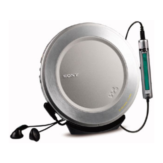
PORTABLE CD PLAYER
UK Model
E Model
Advertisement
Table of Contents

Related Manuals for Sony D-EJ985


Summary of Contents for Sony D-EJ985
- Page 1 ** Charging time varies depending on how the Power requirements rechargeable battery is used. For the area code of the model you *** When using Sony alkaline batteries LR6 (SG) purchased, check the upper left side of the (produced in Japan) bar code on the package.
-
Page 2: Table Of Contents
LINE WITH MARK 0 ON THE SCHEMATIC DIAGRAMS AND IN THE PARTS LIST ARE CRITICAL TO SAFE OPERATION. REPLACE THESE COMPONENTS WITH SONY PARTS WHOSE PART NUMBERS APPEAR AS SHOWN IN THIS MANUAL OR IN SUPPLEMENTS PUB- LISHED BY SONY. -
Page 3: Servicing Notes
D-EJ985 SECTION 1 SERVICING NOTES About CD-Rs/CD-RWs BEFORE REPLACING THE OPTICAL PICK-UP BLOCK Please be sure to check thoroughly the parameters as par the “Op- This CD player can play CD-Rs/CD-RWs recorded in the CD-DA tical Pick-Up Block Checking Procedures” (Part No.: 9-960-027- format*, but playback capability may vary depending on the qual- 11) issued separately before replacing the optical pick-up block. - Page 4 D-EJ985 SERVICE MODE 2. Operation in Service Mode When the Service mode is set, the LCD on the remote commander In the Service mode, this set can check the following. displays the following. 1. Service Mode Setting Method Remote commander LCD display To set the service mode, perform as follows.
- Page 5 D-EJ985 Remote Commander LCD display 010001 (1 time) 040004 (4 times) (For the rest, turn the power off and then turn it on again) • [SOUND] button on remote commander Servo auto adjustment 4. Service Mode Releasing Method To release the service mode, perform as follows.
-
Page 6: General
D-EJ985 SECTION 2 This section is extracted from instruction manual. GENERAL Remote control Locating the controls For details, see pages in parentheses. qd x (stop) button qg Display CD player (front) 1 EXT BATT (external battery)/ DC IN 4.5 V (external power input) -
Page 7: Disassembly
D-EJ985 SECTION 3 DISASSEMBLY • This set can be disassembled in the order shown below. 3-1. DISASSEMBLY FLOW 3-2. UPPER LID (A) SUB ASSY (Page 7) 3-3. CABINET (UPPER) SUB ASSY (Page 8) 3-4. MAIN BOARD, OPTICAL PICK-UP SECTION (CDM-3325ER) (Page 8) Note: Follow the disassembly procedure in the numerical order given. -
Page 8: Cabinet (Upper) Sub Assy
D-EJ985 3-3. CABINET (UPPER) SUB ASSY 3 claw 2 three screws (B2) 2 four screws (B2) AVLS knob G-PROTECTION knob 3 claw 1 screw (B2) 3 claw 7 spring (upper lid-2702) 4 cabinet (upper) sub assy 5 Remove the solder. -
Page 9: Electrical Check
D-EJ985 SECTION 4 ELECTRICAL CHECK Focus Bias Check The CD section adjustments are done automatically in this set. In case of operation check, confirm that focus bias. Condition: • Hold the set in horizontal state. Precautions for Check 1. Perform check in the order given. -
Page 10: Diagrams
D-EJ985 SECTION 5 DIAGRAMS 5-1. BLOCK DIAGRAM – MAIN Section (1/2) – RF AMP, DIGITAL SIGNAL PROCESSOR, DIGITAL SERVO PROCESSOR, D-RAM CONTROLLER IC601 DETECTOR WDCK DOUT DIGITAL DOUT WFCK (Page 11) D-RAM IC602 RFDC RFAC XTAO D0-D3 XTAI VCPU B+... -
Page 11: Block Diagram - Main Section (2/2)
D-EJ985 5-2. BLOCK DIAGRAM – MAIN Section (2/2) – B+ SWITCH VCC3 Q301 DOUT (Page 10) J301 OPTICAL TRANSCEIVER LINE OUT (OPTICAL) AOUTL AOUTR (Page 10) (LINE OUT JACK) MUTING Q303 J302 HEADPHONE AMP IC301 IN_L OUT_L IN_R OUT_R (Page 10) -
Page 12: Block Diagram - Power Section
D-EJ985 5-3. BLOCK DIAGRAM – POWER Section – (Page 10) POWER CONTROL IC403 (2/2) PAPC (Page 10) SYNC SYNC (Page 10) SDTO DATA BATM1 (Page 10) CHARGING BATTERY BATM2 CLOCK VOLTAGE DETECTOR (Page 10) CHGSW CIRCUIT CHGMNT VLGO4 LINEAR (Page 10) -
Page 13: Note For Printed Wiring Boards And Schematic Diagrams
D-EJ985 5-4. NOTE FOR PRINTED WIRING BOARDS AND SCHEMATIC DIAGRAMS • Waveforms 6 IC601 ik (RFDC) (CD play mode) 1 IC404 9 (CLK) Note on Printed Wiring Board Note on Schematic Diagram: • X : parts extracted from the component side. -
Page 14: Main Board (Component Side)
D-EJ985 5-5. PRINTED WIRING BOARD – MAIN Board (Component Side) – • Semiconductor Location Ref. No. Location D402 E-10 RECHARGEABLE D406 BATTERY D407 NH-14WM 2PCS. 2.4V D408 D801 D803 R421 D804 R444 D805 IC405 R413 R411 R416 IC602 Q301 C411... -
Page 15: Printed Wiring Board - Main Board (Conductor Side)
D-EJ985 5-6. PRINTED WIRING BOARD – MAIN Board (Conductor Side) – • Semiconductor MAIN BOARD (CONDUCTOR SIDE) Location Ref. No. Location D303 D304 D305 D306 D307 D401 D401 D D S D403 F-11 R484 Q417 D404 Q416 D405 C405 Q403... -
Page 16: Schematic Diagram - Main Board (1/3)
D-EJ985 5-7. SCHEMATIC DIAGRAM – MAIN Board (1/3) – • • See page 13 for Waveforms. See page 19 for IC Block Diagrams. (Page 17) (Page 18) The components identified by mark 0 or dotted line with mark 0 are critical for safety. -
Page 17: Schematic Diagram - Main Board (2/3)
D-EJ985 5-8. SCHEMATIC DIAGRAM – MAIN Board (2/3) – • See page 13 for Waveform. (Page 16) (Page 18) -
Page 18: Schematic Diagram - Main Board (3/3)
D-EJ985 5-9. SCHEMATIC DIAGRAM – MAIN Board (3/3) – • See page 13 for Waveforms. (Page 16) (Page 17) - Page 19 D-EJ985 • IC Block Diagrams IC301 TA2152FN (EL) C-AMP SW BEEP PW/MUTE SW BIAS IC404 TB2127AFN (EL) SYNC 24 PWM XBRK 23 APWM – TRIANGULAR 22 AGND WAVE GENERATING 21 VG CONTROL DGND 20 COM – XRST 19 UI –...
-
Page 20: Ic Pin Function Description
D-EJ985 5-10. IC PIN FUNCTION DESCRIPTION • IC403 TB2130AF (FOCUS/TRACKING COIL DRIVER, SLED MOTOR DRIVER, POWER CONTROL) Pin No. Pin Name Description VREF Reference voltage input terminal RF41 Power supply 4 (APC) section operational amplifier 1 output PAPC Power supply 4 (APC) section operational amplifier 1 non-invert input... - Page 21 D-EJ985 Pin No. Pin Name Description Battery charge circuit error amplifier non-invert input terminal for rechargeable battery INP1 Not used INW1 Battery charge circuit error amplifier invert input for rechargeable battery Battery charge circuit error amplifier output for rechargeable battery...
- Page 22 D-EJ985 • C601 CXD3039AR (RF AMP, DIGITAL SIGNAL PROCESSOR, DIGITAL SERVO PROCESSOR, D-RAM CONTROLLER) Pin No. Pin Name Description XRAS Row address strobe signal output to the D-RAM Data input enable signal output to the D-RAM 3 to 6 D1, D0, D3, D2...
- Page 23 D-EJ985 Pin No. Pin Name Description 53, 54 AVSS1, AVSS2 — Ground terminal (analog system) VREFR R-ch reference voltage output terminal AOUT2 R-ch analog audio signal output AVDD2 — Power supply terminal (analog system) TES1 Input terminal for the test (normally: fixed at “L”) TEST Input terminal for the test (normally: fixed at “L”)
- Page 24 D-EJ985 Pin No. Pin Name Description SFDR Sled servo drive signal (+) output to the TB2130AF SSTP Disc inner position detection signal input terminal Not used Spindle motor drive signal output to the spindle motor driver Spindle motor servo control signal output to the spindle motor driver C176 176.4 kHz clock signal output to the power control and spindle motor driver...
- Page 25 D-EJ985 • IC801 T5AJ4-4H37 (SYSTEM CONTROLLER) Pin No. Pin Name Description — Ground terminal (digital system) System clock input from the CXD3039AR XOUT High frequency oscillator output terminal Not used TEST Test terminal for IC Not used VCPU — Power supply terminal Digital output LED control signal output “L”: ON...
- Page 26 D-EJ985 Pin No. Pin Name Description 61 to 63 V3 to V1 Liquid crystal display drive bias control signal output terminal Not used Terminal for doubler circuit capacitor connection to develop liquid crystal display drive voltage 64, 65 C1, C0...
-
Page 27: Exploded Views
D-EJ985 SECTION 6 EXPLODED VIEWS NOTE: • -XX and -X mean standardized parts, so they • Items marked “*” are not stocked since they The components identified by mark 0 or dotted line with mark may have some difference from the original are seldom required for routine service. -
Page 28: Cabinet (Lower) Section
D-EJ985 6-2. CABINET (LOWER) SECTION CDM-3325ER R410 Ref. No. Part No. Description Remark Ref. No. Part No. Description Remark X-3382-561-1 CABINET (LOWER) ASSY (L) (BLUE) * 54 A-3347-678-A MAIN BOARD, COMPLETE (for SILVER) (EXCEPT KR) (EXCEPT UK) X-3382-562-1 CABINET (LOWER) ASSY (S) (SILVER) -
Page 29: Optical Pick-Up Section (Cdm-3325Er)
D-EJ985 6-3. OPTICAL PICK-UP SECTION (CDM-3325ER) M902 M901 The components identified by mark 0 or dotted line with mark 0 are critical for safety. Replace only with part number specified. Ref. No. Part No. Description Remark Ref. No. Part No. -
Page 30: Electrical Parts List
D-EJ985 SECTION 7 ELECTRICAL PARTS LIST MAIN NOTE: • Due to standardization, replacements in the • RESISTORS The components identified by mark 0 or dotted line with mark parts list may be different from the parts speci- All resistors are in ohms. - Page 31 D-EJ985 MAIN Ref. No. Part No. Description Remark Ref. No. Part No. Description Remark C464 1-164-156-11 CERAMIC CHIP 0.1uF < DIODE > C465 1-125-777-11 CERAMIC CHIP 0.1uF D303 8-719-422-37 DIODE MA8051-TX C466 1-104-847-11 TANTALUM CHIP 22uF D304 8-719-422-37 DIODE MA8051-TX...
- Page 32 D-EJ985 MAIN Ref. No. Part No. Description Remark Ref. No. Part No. Description Remark L403 1-414-404-11 INDUCTOR 100uH R409 1-218-965-11 RES-CHIP 1/10W L404 1-419-188-41 INDUCTOR 100uH R411 1-216-308-00 RES-CHIP 1/10W L405 1-414-404-11 INDUCTOR 100uH L406 1-400-145-21 INDUCTOR 47uH R413 1-217-671-11 METAL CHIP...
- Page 33 D-EJ985 MAIN Ref. No. Part No. Description Remark Ref. No. Part No. Description Remark R605 1-218-990-11 SHORT CHIP S806 1-786-407-41 SWITCH, PUSH (3 DIRECTION) (GRAY) R606 1-218-969-11 RES-CHIP 1/10W (. >, N X) (for BLUE, RED) R607 1-218-969-11 RES-CHIP 1/10W...
- Page 34 D-EJ985 Ref. No. Part No. Description Remark Ref. No. Part No. Description Remark ACCESSORIES *********** 1-477-464-11 REMOTE COMMANDER (RM-MC32EL) 1-477-496-11 ADAPTOR, AC (AC-ES455K) (JE) 1-477-497-11 ADAPTOR, AC (AC-ES455K) (KR) 1-477-499-11 ADAPTOR, AC (AC-ES455K) (CH) 1-477-500-11 ADAPTOR, AC (AC-ES455K) (E) 1-477-501-11 ADAPTOR, AC (AC-ES455K) (UK, HK)
- Page 35 D-EJ985 MEMO...
-
Page 36: Revision History
D-EJ985 REVISION HISTORY Clicking the version allows you to jump to the revised page. Also, clicking the version at the upper right on the revised page allows you to jump to the next revised page. Ver. Date Description of Revision...