Table of Contents
Advertisement
Quick Links
SERVICE MANUAL
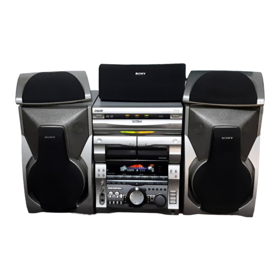
HCD-V919AV is the Amplifier, Video CD
player, Tape Deck and Tuner section in
MHC-V919AV.
This stereo system is equipped with the Dolby B-
type noise reduction system and Dolby Pro Logic
Surround decoder*.
* Manufactured under license from Dolby Labora-
tories Licensing Corporation.
DOLBY, the double-D symbol a and "PRO LOGIC"
are trademarks of Dolby Laboratories Licensing Cor-
poration.
MICROFILM
HCD-V919AV
Model Name Using Similar Mechanism
CD Mechanism Type
CD
Section
Base Unit Name
Optical Pick-up Name
Model Name Using Similar Mechanism
Tape
Deck
Tape Transport Mechanism Type
Section
SPECIFICATIONS
MINI Hi-Fi COMPONENT SYSTEM
E Model
Chinese Model
HCD-V717
CDM38L-5BD24AL
BU-5BD24AL
KSS-213D/Q-NP
HCD-V717
TCM-230AWR1/
230PWR1
– Continued on next page –
Advertisement
Table of Contents

Related Manuals for Sony HCD-V919AV


Summary of Contents for Sony HCD-V919AV
- Page 1 HCD-V919AV SERVICE MANUAL E Model Chinese Model HCD-V919AV is the Amplifier, Video CD player, Tape Deck and Tuner section in MHC-V919AV. This stereo system is equipped with the Dolby B- Model Name Using Similar Mechanism HCD-V717 type noise reduction system and Dolby Pro Logic...
- Page 2 HCD-V919AV 7-9. SCHEMATIC DIAGRAM – BD Section – • See page 86 for Waveforms. • See page 90 and 91 for IC Block Diagrams. (Page 43) The components identified by mark ! or dotted line with mark ! are critical for safety.
- Page 3 HCD-V919AV 7-11. SCHEMATIC DIAGRAM – VIDEO Section (1/2) – • See page 91 for IC Block Diagram. (Page 39) (Page 62) (Page 45) • Voltages and waveforms are dc with respect to ground in *Note VIDEO CD play mode. When replacing IC502, refer to “IC502 of no mark : VIDEO CD play VIDEO board”...
- Page 4 HCD-V919AV 7-12. SCHEMATIC DIAGRAM – VIDEO Section (2/2) – • See page 86 to 88 for Waveforms. • See page 91 for IC Block Diagram. (Page 43) – 45 – – 46 –...
- Page 5 HCD-V919AV 7-14. SCHEMATIC DIAGRAM – CD MOTOR Section – • See page 92 for IC Block Diagrams. MAIN BOARD CN104 (Page 62) MAIN BOARD CN103 (Page 62) – 49 – – 50 –...
- Page 6 HCD-V919AV 7-16. SCHEMATIC DIAGRAM – TAPE DECK Section – • See page 92 for IC Block Diagram. MAIN BOARD CN106 (Page 60) The components identified by mark ! or dotted line with mark ! are critical for safety. Replace only with part number specified.
- Page 7 HCD-V919AV 7-17. PRINTED WIRING BOARD – LEAF SW Section – • See page 35 for Circuit Boards Location. MAIN BOARD CN107 (Page 57) 7-18. SCHEMATIC DIAGRAM – LEAF SW Section – MAIN BOARD CN107 (Page 60) – 55 – – 56 –...
- Page 8 HCD-V919AV 7-20. SCHEMATIC DIAGRAM – MAIN Section (1/4) – (Page 56) (Page 54) (Page 61) (Page 61) (Page 65) (Page 65) (Page 61) (Page 63) (Page 63) (Page 65) • Voltages and waveforms are dc with respect to ground under no-signal (detuned) conditions.
- Page 9 HCD-V919AV 7-21. SCHEMATIC DIAGRAM – MAIN Section (2/4) – • See page 88 for Waveforms. (Page 60) (Page 43) (Page 60) (Page 50) (Page 50) (Page 60) • Voltages and waveforms are dc with respect to ground under no-signal (detuned) conditions.
- Page 10 HCD-V919AV 7-22. SCHEMATIC DIAGRAM – MAIN Section (3/4) – • See page 93 for IC Block Diagrams. (Page 59) (Page 59) (Page 65) (Page 65) (Page 65) (Page 62) (Page 85) • Voltages and waveforms are dc with respect to ground under no-signal (detuned) conditions.
- Page 11 HCD-V919AV 7-23. SCHEMATIC DIAGRAM – MAIN Section (4/4) – (Page 61) (Page 61) (Page 61) (Page 62) (Page 60) (Page 60) (Page 60) (Page 64) (Page 64) (Page 64) (Page 69) (Page 79) (Page 79) • Voltages and waveforms are dc with respect to ground under no-signal (detuned) conditions.
- Page 12 HCD-V919AV • Voltages and waveforms are dc with respect to ground under no-signal (detuned) conditions. 7-25. SCHEMATIC DIAGRAM – PANEL Section – • See page 89 for Waveforms. • See page 92 for IC Block Diagrams. no mark : FM...
- Page 13 HCD-V919AV 7-27. SCHEMATIC DIAGRAM – DISPLAY Section – (Page 70) (Page 69) (Page 70) • Voltages and waveforms are dc with respect to ground under no-signal (detuned) conditions. no mark : FM – 73 – – 74 –...
- Page 14 HCD-V919AV 7-28. SCHEMATIC DIAGRAM – MIC/HEADPHONE Section – 7-29. PRINTED WIRING BOARDS – MIC/HEADPHONE Section – • See page 92 for IC Block Diagrams. • See page 35 for Circuit Boards Location. (Page 78) (Page 79) (Page 77) (Page 79) •...
- Page 15 HCD-V919AV 7-31. SCHEMATIC DIAGRAM – POWER AMP Section – (Page 75) (Page 81) (Page 66) (Page 81) (Page 75) (Page 81) (Page 66) (Page 81) (Page 81) • Voltages and waveforms are dc with respect to ground The components identified by mark ! or dotted under no-signal (detuned) conditions.
- Page 16 HCD-V919AV 7-32. SCHEMATIC DIAGRAM – TRANSFORMER Section – • See page 83 for Printed Wiring Board. (POWER BOARD) • See page 83 for Printed Wiring Board. (TRANSFORMER BOARD) (Page 80) (Page 80) (Page 80) (Page 80) (Page (Page 80) • Voltages and waveforms are dc with respect to ground The components identified by mark ! or dotted under no-signal (detuned) conditions.
- Page 17 HCD-V919AV 7-35. SCHEMATIC DIAGRAM – SURROUND Section – (Page 63) (Page • Voltages and waveforms are dc with respect to ground The components identified by mark ! or dotted under no-signal (detuned) conditions. line with mark ! are critical for safety.
- Page 18 • Waveforms – BD Board – 1 IC101 @§ (RFDC) – VIDEO Board – 6 IC101 $¶ (BCLK) 1 IC501 5 (LRCK) 200 mV/DIV, 500 ns/DIV +0.25 Vp-p –0.20 5.2 Vp-p 5 Vp-p 474 ns 22.8 s 2 IC101 @¶ (TE) !£...
- Page 19 !ª &∞ !§ IC505 `⁄⁄⁄ (DA-BCK), IC509 !¶ (BCK) 6 IC402 !¡ IC505 (XIN) (C-OUT) 0.5 Vp-p 4.8 Vp-p 3.4 Vp-p 8.1 MHz 472 ns @º 7 IC402 *§ !™ IC505 !¶ Q301 (Base) (XOUT) (DA-XCLK) 1.8 Vp-p 4.2 Vp-p 5.2 Vp-p 8.1 MHz 60 ns...
- Page 20 – MAIN Board – @§ IC401 3 @¡ IC509 @º (384FSO) 1 IC501 0 (X2) 5.1 Vp-p 1 Vp-p 5.5 Vp-p 5 MHz 59 ns @™ IC509 @¡ (768FSO) @¶ IC401 1 2 IC501 !£ (XT2) 4.8 Vp-p 5 Vp-p 2 Vp-p 32.768 kHz 30 ns...
- Page 21 – PANEL Board – 1 IC601 8 (X-OUT) 4 Vp-p 8 MHz 2 IC801 2 (X-OUT) 4.3 Vp-p 8 MHz 3 IC851 2 (XT) 3.6 Vp-p 4.09 MHz – 89 –...
-
Page 22: Ic Block Diagrams
• IC Block Diagrams – BD Board – IC101 CXD2545Q 61 – 51 DA16 EXCK DA12 LRCK WDCK SQSO PSSL SQCK MUTE SENS XRST DIRC ASYE SCLK DFSW ATSK AVDD ASYO DATA XLAT CLOK ASYI MIRR DFCT BIAS RFAC AVSS CLTV FILI LOCK... -
Page 23: Video Board
IC103 CXA1821M-T6 LD ON LC/PD APC LD AMP VREF RF EQ AMP RF SUMMING AMP FOCUS ERROR AMP FE BIAS TRACKING ERROR AMP VC BUFFER –VIDEO Board – IC509 PCM1727E-2/T2 384fs CLOCK MANAGER • DUAL PLL DGND PGND POWER SUPPLY SCKO1 SCKO2 NCKO... -
Page 24: Panel Board
– MOTOR (TURN) Board – – PANEL Board – IC701 M54641L IC603 BA3833F-E2 RESET 18 RESET RESET REFERENCE REFFERENCE PREF 17 f01 POWER OUT2 INPUT CURRENT AMP. AMP. CONTROL LINE 16 f02 POWER OUT1 INPUT AMP. AMP. LINE 15 f03 BIAS 13 f Bias... - Page 25 – MAIN Board – IC201 LV1041M R BPF2 L BPF2 RECT RECT LOGIC LOGIC R BPF1 RECT RECT L BPF1 LOGIC LOGIC RT IN S DC OUT C DC OUT R DC OUT LT IN L DC OUT CONTROL DC CUT V REF V REF CONTROL...