Table of Contents
Advertisement
CDP-CX400/CX450
SERVICE MANUAL
Ver 1.1 2001. 10
Sony Corporation
9-929-232-12
2001J1600-1
Home Audio Company
© 2001.10
Published by Sony Engineering Corporation
Photo; CDP-CX400
Model Name Using Similar Mechanism
CD Mechanism Type
Base Unit Type
Optical Pick-up Type
SPECIFICATIONS
USA, Canadian
Europian
US Model
Canadian Model
CDP-CX400/CX450
AEP Model
UK Model
Australian Model
NEW
CDM62-K1BD35A
BU-K1BD35A
KSM-213BFN
230 V AC, 50/60 Hz
COMPACT DISC PLAYER
E Model
CDP-CX450
Advertisement
Table of Contents

Related Manuals for Sony CDP-CX400; CDP-CX450


Summary of Contents for Sony CDP-CX400; CDP-CX450
- Page 1 Model Name Using Similar Mechanism CD Mechanism Type CDM62-K1BD35A Base Unit Type BU-K1BD35A Optical Pick-up Type KSM-213BFN SPECIFICATIONS USA, Canadian Europian 230 V AC, 50/60 Hz COMPACT DISC PLAYER Sony Corporation 9-929-232-12 2001J1600-1 Home Audio Company © 2001.10 Published by Sony Engineering Corporation...
- Page 2 PIÈCES SONT CRITIQUES POUR LA SÉCURITÉ DE • Abbreviation FONCTIONNEMENT. NE REMPLACER CES COMPOSANTS CND : Canadian model QUE PAR DES PIÈCES SONY DONT LES NUMÉROS AUS : Australian model : Singapore model. SONT DONNÉS DANS CE MANUEL OU DANS LES MY : Malaysia model.
-
Page 3: Table Of Contents
SECTION 1 SERVICE NOTE TABLE OF CONTENTS NOTES ON HANDLING THE OPTICAL PICK-UP BLOCK OR BASE UNIT 1. SERVICING NOTE ............3 The laser diode in the optical pick-up block may suffer electrostatic 2. GENERAL ................6 break-down because of the potential difference generated by the charged electrostatic load, etc. - Page 4 CD-TEXT TEST DISC This unit is able to display the TEXT data (character information) written in the CD on its fluorescent indicator tube. The CD-TEXT TEST DISC (TGCS-313:J-2501-126-A) is used for checking the display. To check, perform the following procedure. Checking Method: Turn ON the power, set the disc on the disc table with the side labeled as “test disc”...
- Page 5 Table 2: CD-TEXT TEST DISC Recorded Contents and Display (In this unit, some special characters cannot be displayed. This is no a fault.) TRACK Recorded contents Display N All the same ! ” # $ % & ´ (21h to 27h)1kHz 0dB L&R N All the same + , –...
-
Page 6: General
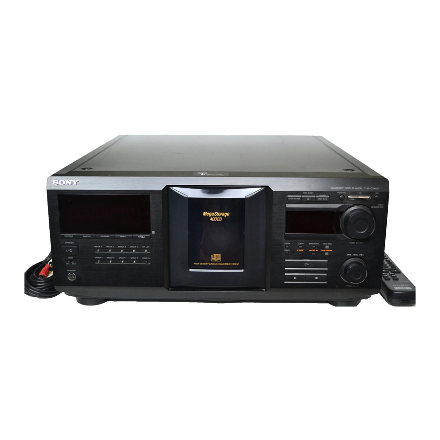
SECTION 2 GENERAL Front Panel q;qaqs qd qf qg qk ql ws wd ejeheg eae; wk wjwh Photo: CDP-CX400 LOCATION OF PARTS AND CONTROLS 1 1/u (power) button wa FADER button 2 STANDBY indicator ws X-FADE button 3 Display window wd NO DELAY button 4 CONTINUE button wf MEGA CONTROL button and indicator... -
Page 7: Disassembly
SECTION 3 DISASSEMBLY Note : Follow the disassembly procedure in the numerical order given. 3-1. UPPER CASE 1 Three screws (case 3 screw) 2 Two screws @ (case 3 screw) 3 Two screws @ (case 3 screw) 5 Upper Case 4 Two screws @ (case 3 screw) 3-2. -
Page 8: Front Panel Assembly
3-3. FRONT PANEL ASSEMBLY 1 Connector (CNP503) 2 Screw (BVTP 3 5 Remove the claw 3 Two screws (BVTP 3 6 Remove the claw 7 Front panel assembly 4 Three screws (BVTP 3 3-4. TABLE (400) ASSEMBLY 3 Table (400) assembly 1 Screw (BVTP 3 2 Guide (door) 4 Washer... -
Page 9: Base (Door, Driving) Assembly
3-5. BASE (DOOR DRI VING) ASSEMBLY 1 Two screws (BVTP 3 5 Cover (table) 4 Three screws (BVTP 3 2 Cover (PT) 9 Base (door driveing) assembly 6 Door assembly 3 Connector (CN602) 7 Two screws (BVTP 3 8 Eight screws (BVTP 3 3-6. -
Page 10: Back Panel Assembly
3-7. BACK PANEL ASSEMBLY 2 Cover (CDM) 1 Nine screws (BVTP 3 3 Three screws (BVTP 3 4 Bracket (CDM) 6 Four screws (BVTP 3 7 Back panel assembly 5 Connector (CN991) 3-8. CDM ASSEMBLY 5 Magnet assembly 3 Six screws (BVTP 3 6 Washer 8 CD mechanism 7 Spring... -
Page 11: Service Mode
SECTION 4 SERVICE MODE SPECIAL FUNCTION This unit is provided with several service modes. Details are shown in the following table. Turn on the power and press GROUP FILE , MEGA CONTROL and 1/u buttons. Rotate the DISC/CHARACTER dial to enter any of the following modes. Display Mech Adjust Mechanism adjustment mode... - Page 12 Special Aging Mode Functions Aging Procedure The aging mode is provided with the following convenient func- Turn on the power and press the GROUP FILE , MEGA CONTROL and 1/u buttons. tions • Disc setting mode (*1) Rotate DISC/CHARACTER dial, select “Normal Aging” and •...
- Page 13 LOADING AGING MODE TITLE MEMO SHIFT MODE • This mode is used for repeating loading operations continuously. • This mode is used for writing title memo information recorded in • Aging will be performed continuously unless an error occurs. this unit in a different unit. •...
- Page 14 MECHANISM ADJUSTMENT MODE • This mode is used for mechanism adjustments. Refer to the section on Mechanism Adjustments. SHIPMENT MODE • This mode is used for setting the unit to the shipment state. Do not execute it without a proper reason as it erases the memory of the title memo recorded by the customer.
-
Page 15: Test Mode
SECTION 5 TEST MODE 5-1. ADJ Mode 5-2. Key and Display Check Mode Turn ON the power of the unit, set disc to disc table, and perform To set this mode, connect the test point (AFADJ) on the MAIN chucking. board to Ground, and connect the power supply plug to the outlet. -
Page 16: Adjustments
SECTION 6 ADJUSTMENTS 6-1. MechaniCAL Adjustments Pop Up Mechanism Adjustment Turn on the power and set the dick to number 24. With the power ON, while pressing the GROUP FILE and MEGA CONTROL buttons, press the 1/u button to enter the Adjastment mode. - Page 17 Sensor Adjustment Enter the adjustment mode and select “Mech Adjust” with the JOG dial, and press the dial. Press the GROUP 1 button to operate the loading mechanism, and continue pressing until the disc table locks. (Fig-3) Loosen the fixing screw and move the holder so that both PLAY button LED (green) and the ARTIST MODE button LED (green) light.
-
Page 18: Electrical Adjustment
6-2. ELECTRICAL ADJUSTMENT Note: A clear RF signal waveform means that the shape “ ” can be clearly distinguished at the center of the waveform. Note: RF signal waveform CD Block is basically designed to operate without adjustment. Therefore, check each item in order given. VOLT/DIV : 200mV Use YEDS-18 disc (3-702-101-01) unless otherwise indicated. - Page 19 Disc Sensor Adjustment Rotate the DISC/CHARACTER knob in the counterclockwise Be sure to perform this adjustment after sensor adjustment in direction and the disc table starts to rotate in the same direction. MECHANICAL ADJUSTMENT. Check that the waveform at this time is the same as that in step 4.
-
Page 20: Diagrams
SECTION 7 DIAGRAMS 7-1. CIRCUIT BOARDS LOCATION LED board MAIN board D. SENS (IN) board DISPLAY board TRANS board D. SENS (OUT) board KEY board T. SENS board D. MOTOR board DOOR SW board JOG board BD board LOADING SW board L. -
Page 21: Block Diagrams
CDP-CX400/CX450 7-2. BLOCK DIAGRAMS – BD SECTION – IC101 OPTICAL PICK-UP DIGITAL SERVO BLOCK IC103 DIGITAL SIGNAL PROC. (KSM-213BFN) IC901 J903 RF AMP D/A CONV. DIGITAL DIGITAL D OUT CD IN OPTICAL MUTE RFAC IC401 IC302 IC302 Q324 RFDC LINE L OUT MUTE R-CH... -
Page 22: Main Section
CDP-CX400/CX450 – MAIN SECTION – IC501(2/2) SYSTEM CONTROL FL701 FL702 FLUORESCENT FLUORESCENT INDICATOR TUBE INDICATOR TUBE . D0 IC701 FL DRIVER IC504 FL DATA SRAM DIG1 FL CLK FL T1 DIG15 65 71 RESET Q701 DIG16 SEG01 SEG35 AD1(36) Q521 IC702 FL DRIVER D701-712,715... - Page 23 CDP-CX400/CX450 Waveforms THIS NOTE IS COMMON FOR PRINTED WIRING BOARDS AND SCHEMATIC DIAGRAMS. IC101 wh MDP IC101 yj XTAI (In addition to this, the necessary note is printed in each block.) 2.4Vp-p 3.1Vp-p For schematic diagrams. Note: • All capacitors are in µF unless otherwise noted. pF: µµF 16.9MHz 7.5 sec 50 WV or less are not indicated except for electrolytics...
-
Page 24: Schematic Diagram - Bd Section
CDP-CX400/CX450 7-3. Schematic Diagram – BD Section – • See page 23 for Waveforms. • See page 36 for IC Block Diagrams. • See page 38 for IC Pin Functions. KSM-213BFN PIN FUNCTION MAIN BOARD (Page 27) The components identified by Les composants identifiés par mark 0 or dotted line with mark une marque 0 sont critiques... -
Page 25: Printed Wiring Board - Bd Section
CDP-CX400/CX450 7-4. Printed Wiring Board – BD Section – • See page 20 for Circuit Boards Location. KSM-213BFN MAIN BOARD (Page 26) • Semiconductor Location Ref. No. Location IC101 IC102 IC103 Q101... -
Page 26: Printed Wiring Board - Main Section
CDP-CX400/CX450 7-5. Printed Wiring Board – MAIN Section – • See page 20 for Circuit Boards Location. • Semiconductor Location (Page 35) (Page 29) (Page 35) (Page 35) (Page 31) Ref. No. Location D327 D329 D501 D521 D580 D941 D942 IC302 IC401 IC402... -
Page 27: Schematic Diagram - Main (1/2) Section
CDP-CX400/CX450 Ver 1.1 2001.10 7-6. Schematic Diagram – MAIN (1/2) Section – • See page 23 for Waveforms. • See page 36, 37 for IC Block Diagrams. (Page 30) (Page 29) (Page 32) (Page 30) (Page 24) (Page 29) PIN FUNCTION CX400 : M30620MC-407FP CX450 : M30622MGA-309FP (Page 34) -
Page 28: Schematic Diagram - Main (2/2) Section
CDP-CX400/CX450 7-7. Schematic Diagram – MAIN (2/2) Section – • See page 23 for Waveforms. • See page 36 for IC Block Diagrams. • See page 40 for IC Pin Functions. -
Page 29: Printed Wiring Board - T. Sens Section
CDP-CX400/CX450 7-8. Printed Wiring Board – SENSOR Section – 7-9. Schematic Diagram – SENSOR Section – • See page 20 for Circuit Boards Location. MAIN BOARD (Page 26) (Page 27) (Page 27) (Page 26) -
Page 30: Schematic Diagram - Display Section
CDP-CX400/CX450 7-10. Schematic Diagram – DISPLAY Section – • See page 23 for Waveforms. • See page 37 for IC Block Diagrams. (Page 32) (Page 27) (Page 27) -
Page 31: Printed Wiring Board - Display Section
CDP-CX400/CX450 7-11. Printed Wiring Board – DISPLAY Section – • See page 20 for Circuit Boards Location. • Semiconductor (Page 33) (Page 26) Location Ref. No. Location D591 D592 D593 D594 D595 D596 D597 D598 D701 D702 D703 D704 D705 D706 D707 D708... -
Page 32: Schematic Diagram - Jog Section
CDP-CX400/CX450 7-12. Schematic Diagram – JOG Section – • See page 23 for Waveforms. (Page 30) (Page 27) (Page 27) -
Page 33: Printed Wiring Board - Jog Section
CDP-CX400/CX450 7-13. Printed Wiring Board – JOG Section – • See page 20 for Circuit Boards Location. • Semiconductor Location Ref. No. Location D711 D712 (Page 31) D715 IC704 CX450 : AEP,UK,SP, MY,AUS (Page 26) (Page 26) -
Page 34: Schematic Diagram - Power Section
CDP-CX400/CX450 7-14. Schematic Diagram – POWER Section – • See page 23 for Waveforms. • See page 37 for IC Block Diagrams. (Page 27) (Page 27) (Page 27) The components identified by Les composants identifiés par mark 0 or dotted line with mark une marque 0 sont critiques 0 are critical for safety. -
Page 35: Printed Wiring Board - Power Section
CDP-CX400/CX450 7-15. Printed Wiring Board – POWER Section – (Page 26) (Page 26) (Page 26) • Semiconductor Location Ref. No. Location D901 D902 D903 D904 D905 D906 D907 D911 D912 D913 D921 D922 D923 D924 D931 D932 D933 D934 D935 D991 IC941 IC961... -
Page 36: Ic Block Diagrams
CDP-CX400/CX450 7-16. IC BLOCK DIAGRAMS IC103 CXA2568M-T6 (BD BOARD) IC931 BA3993F (MAIN BOARD) IC101 CXD2587Q (BD BOARD) APC PD AMP LC/PD LD_ON HOLD AGCVTH VREF ERROR APC LD AMP DIGITAL CORRECTOR HOLD_SW DIGITAL ASYMMETRY CORRECTION AGCCONT (50%/30% OPERATIONAL OFF) LRCK AMPLIFIER RF_BOT ANALOG SWITCH... -
Page 37: Ic Pin Functions
IC803 CXA2075M (MAIN BOARD) VIDEO TRAP SWITCH DRIVER DRIVER Y/C MIX R-OUT G-OUT B-OUT INTERNAL TRAP SYNC DELAY Modulator REGULATOR Modulator PHASE PULBE CLAMP SIN-PULBE SHIFTER IC702 M66310FP (DISP BOARD) IC941, IC961 LA6510 (TRANS BOARD) – – 1 2 3 4 5 6 7 8 9 10... - Page 38 7-17. IC PIN FUNCTIONS • IC101 DIGITAL SIGNAL PROCESSOR (CXD2587Q) (BD board) Pin Name Function Pin No. SQSO Sub-Q 80-bit and PCM peak level data output (CD text data output) SQCK Clock input for SQSO read-out XRST System reset “L” : reset SYSM Muting input “H”...
- Page 39 Pin No. Pin Name Function Tracking error signal input Center servo analog input RF signal input RFDC Test pin (Not used) ADIO — Analog ground AVSS0 Stabilized current input for operational amplifiers IGEN — Analog power supply AVDD0 EFM full swing output ASYO Asymmetry comparate voltage input ASYI...
- Page 40 Ver 1.1 2001.10 • IC501 SYSTEM CONTROL (M30620MC-407FP) (CX400) (MAIN board) • IC501 SYSTEM CONTROL (M30622MGA-309FP) (CX450) (MAIN board) Pin No. Pin Name Function FLDATA Data output to fluorescent indicator driver FLCLK Clock output to fluorescent indicator driver RM_IN SIRCS input BUSOUT Ctrl-A1 output BUSIN...
- Page 41 Pin Name Function Pin No. JOGB Disc JOG input Interal illumination LED output TOSHIBA_SIRCS Bidirectional microprocessor 455 kHz output enable output (CX450) TOSHIBA_RST Bidirectional microprocessor reset output (C450) TOSHIBA/CE Bidirectional microprocessor bidirectional function ON/OFF(CX450) OPEN — Not used. SRAM address output —...
-
Page 42: Exploded Views
SECTION 8 EXPLODED VIEWS NOTE: The components identified by • The mechanical parts with no reference number • -XX, -X mean standardized parts, so they may mark 0 or dotted line with mark in the exploded views are not supplied. have some difference from the original one. -
Page 43: Chassis Section
Ref. No. Part No. Description Remark Ref. No. Part No. Description Remark 4-226-841-01 COVER(PT) 4-226-838-31 PANEL, BACK (CX450:CND) 4-226-855-11 UPPER CASE 4-226-838-41 PANEL, BACK (CX450:AEP,UK) 4-210-291-01 SCREW(CASE 3 TP2) 4-226-838-51 PANEL, BACK (CX450:AUS) 1-500-386-11 FILTER, CLAMP (FERRITE CORE) 4-226-838-61 PANEL, BACK (CX450:SP,MY) (CX450:US,CND) 1-792-466-11 WIRE(FLAT TYPE) (23 CORE) 1-569-008-21 ADAPTOR, CONVERSION (CX450:SP,MY) -
Page 44: Front Panel Section
8-2. CHASSIS SECTION not supplied not supplied not supplied not supplied CDM62-K1BD35A SECTION-2 CDM62-K1BD35A SECTION-1 CDM62-K1BD35A SECTION-3 Ref. No. Part No. Description Remark Ref. No. Part No. Description Remark X-4952-641-1 DOOR ASSY 1-676-833-11 D.SENS (IN) BOARD 3-356-601-11 SCREW, STEP 4-216-096-01 SCREW (T1), STEP 4-226-834-01 COVER (TABLE) 4-216-089-01 SHAFT (CENTER) 4-226-833-01 GUIDE (DOOR) -
Page 45: Mechanism Section 1 (Cdm54-K1Bd35E)
8-3. FRONT PANEL SECTION FL701 CX450 FL702 CX450 (AEP, UK, SP, MY, AUS) supplied Ref. No. Part No. Description Remark Ref. No. Part No. Description Remark X-4952-636-1 PANEL ASSY, FRONT (CX400) A-4725-036-A DISP BOARD, COMPLETE X-4952-637-1 PANEL ASSY, FRONT (CX450:US,CND) (CX450:AEP,UK,SP,MY,AUS) X-4952-638-1 PANEL ASSY, FRONT A-4725-049-A DISP BOARD, COMPLETE (CX400) -
Page 46: Mechanism Section 2 (Cdm54-K1Bd35E)
8-4. MECHANISM SECTION 1 (CDM62-K1BD35A) M603 Ref. No. Part No. Description Remark Ref. No. Part No. Description Remark 4-226-827-01 BASE (DOOR DRIVING) 4-216-104-01 SPRING (POP-UP), TENSION 4-216-093-01 ROLLER 4-219-326-01 BELT (DIA. 42X1.2) 4-216-100-01 HOLDER (POP-UP) 3-701-441-21 WASHER 4-933-134-11 SCREW (+PTPWH M2.6X8) 4-226-828-01 GEAR (CAM) 4-226-832-01 LEVER (PU JOINT) 4-226-829-01 GEAR (PULLEY) -
Page 47: Mechanism Section 3 (Cdm54-K1Bd35E)
8-5. MECHANISM SECTION 2 (CDM62-K1BD35A) not supplied M601, M602 not supplied Ref. No. Part No. Description Remark Ref. No. Part No. Description Remark A-4672-895-A MOTOR (400) ASSY 4-225-865-01 SLIDER (400) 4-951-620-01 SCREW (2.6X8), +BVTP A-4672-676-B CAMASSY 1-676-837-11 L.T.MOTOR BOARD 4-216-058-01 GEAR (CENTER) 4-933-134-11 SCREW (+PTPWH M2.6X8) 4-216-057-01 GEAR (CENTER 2) 1-676-835-11 LOCK SW BOARD... -
Page 48: Opeical Pick-Up Section (Ksm-213Bfn/M-Np)
8-6. MECHANISM SECTION 3 (CDM62-K1BD35A) 256 255 Ref. No. Part No. Description Remark Ref. No. Part No. Description Remark 3-325-697-21 WASHER X-4952-502-1 HOLDER (DISC R400) ASSY 4-216-078-01 LEVER (LOADING) X-4952-501-1 HOLDER (DISC L400) ASSY 4-216-079-02 LIMITTER (LEVER) X-4952-499-1 LEVER (LOCK 400) ASSY 4-216-080-01 SPRING (LIMITTER), TORSION X-4950-901-5 HOLDER ASSY, BU X-4950-900-1 BRACKET (LEVER) ASSY... -
Page 49: Electrical Parts List
SECTION 9 ELECTRICAL PARTS LIST Note: • Due to standardization, replacements in the parts • SEMICONDUCTORS The components identified by In each case, u: µ , for example: list may be different from the parts specified in the mark ! or dotted line with mark uA...: µ... - Page 50 DISP Ref. No. Part No. Description Remarks Ref. No. Part No. Description Remarks R111 1-216-121-91 RES-CHIP 1/10W C596 1-162-306-11 CERAMIC 0.01uF 20.00% 16V R113 1-216-121-91 RES-CHIP 1/10W (CX450) R116 1-216-025-91 RES-CHIP 1/10W C781 1-104-665-11 ELECT 100uF 20.00% 10V R117 1-216-049-91 RES-CHIP 1/10W C782 1-104-665-11 ELECT...
- Page 51 DISP DOOR SW D.MOTOR D.SENS(IN) D.SENS(OUT) Ref. No. Part No. Description Remarks Ref. No. Part No. Description Remarks < RESISTOR > S766 1-771-349-21 SWITCH, KEYBOARD (STANDBY) S768 1-570-157-51 SWITCH, SLIDE (TIMER) R591 1-249-383-11 CARBON 1/6W F ************************************************************ (CX450) R592 1-249-383-11 CARBON 1/6W F 1-676-838-11 DOOR SW BOARD (CX450)
- Page 52 Ref. No. Part No. Description Remarks Ref. No. Part No. Description Remarks C751 1-161-494-00 CERAMIC 0.022uF < SWITCH > C773 1-164-159-11 CERAMIC 0.1uF C774 1-124-584-00 ELECT 100uF S701 1-771-349-21 SWITCH, KEYBOARD (OPEN/CLOSE) C775 1-162-207-31 CERAMIC 22PF S702 1-771-349-21 SWITCH, KEYBOARD (EJECT) C776 1-164-159-11 CERAMIC 0.1uF...
- Page 53 LOADING SW LOCK SW L.T.MOTOR MAIN Ref. No. Part No. Description Remarks Ref. No. Part No. Description Remarks 1-676-840-11 LED BOARD C321 1-126-963-11 ELECT 4.7uF 20.00% 50V C327 1-124-282-00 ELECT 22uF 20.00% 25V ********* C328 1-162-290-31 CERAMIC 470PF 4-976-473-01 HOLDER (LED-S) C329 1-126-962-11 ELECT 3.3uF...
- Page 54 Ver 1.1 2001.10 MAIN Ref. No. Part No. Description Remarks Ref. No. Part No. Description Remarks C818 1-104-665-11 ELECT 100uF 20.00% 10V C951 1-164-159-11 CERAMIC 0.1uF (CX450) C952 1-164-159-11 CERAMIC 0.1uF C819 1-164-159-11 CERAMIC 0.1uF C953 1-104-664-11 ELECT 47uF 20.00% 16V (CX450) C954 1-164-159-11 CERAMIC...
- Page 55 MAIN Ref. No. Part No. Description Remarks Ref. No. Part No. Description Remarks < COIL > R327 1-249-441-11 CARBON 100K 1/4W R328 1-249-441-11 CARBON 100K 1/4W L501 1-410-396-41 INDUCTOR 0.45uH R329 1-249-441-11 CARBON 100K 1/4W L801 1-408-613-31 INDUCTOR 68uH (CX450) R339 1-215-485-00 METAL 470K...
- Page 56 MAIN TRANS Ref. No. Part No. Description Remarks Ref. No. Part No. Description Remarks R535 1-249-429-11 CARBON 1/4W R831 1-215-421-00 METAL 1/4W R570 1-249-425-11 CARBON 4.7K 1/4W F (CX450) R571 1-249-425-11 CARBON 4.7K 1/4W F R861 1-215-445-00 METAL 1/4W R580 1-249-429-11 CARBON 1/4W (CX450:AEP,UK,SP,MY,AUS)
- Page 57 TRANS Ref. No. Part No. Description Remarks Ref. No. Part No. Description Remarks C921 1-126-768-11 ELECT 2200uF 20.00% 16V < COIL > C922 1-126-768-11 ELECT 2200uF 20.00% 16V C930 1-161-494-00 CERAMIC 0.022uF 0 L991 1-424-485-11 FILTER, LINE C931 1-126-768-11 ELECT 2200uF 20.00% 16V C932...
- Page 58 CDP-CX400/CX450 TRANS T.SENS Ref. No. Part No. Description Remarks Ref. No. Part No. Description Remarks 0 T901 < RELAY > 1-433-877-11 TRANSFORMER, POWER (CX450:AUS) 0 T911 1-435-327-11 TRANSFORMER, POWER (CX400/ 0 RY991 1-755-299-11 RELAY CX450:US,CND) 0 T911 1-435-328-11 TRANSFORMER, POWER <...
- Page 59 CDP-CX400/CX450 MEMO...
- Page 60 CDP-CX400/CX450 REVISION HISTORY Clicking the version allows you to jump to the revised page. Also, clicking the version at the upper right on the revised page allows you to jump to the next revised page. Ver. Date Description of Revision 2001.10 Correction of Part No.