Sony BDP-BX1 Service Manual
Blu-ray disc/dvdplayer
Hide thumbs
Also See for BDP-BX1:
- Service manual (129 pages) ,
- Operating instructions manual (79 pages) ,
- Specifications (2 pages)
Table of Contents
Advertisement
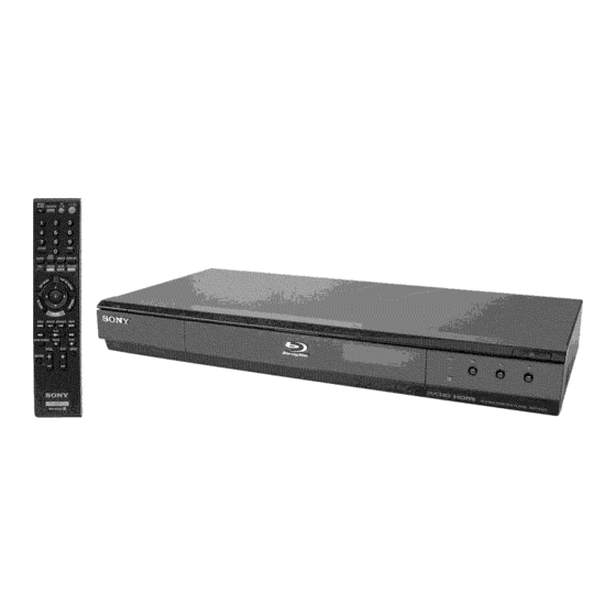
BDP-BX1/S35
RMT-B102A/B102P/B103A
SERVICE
MANUAL
Ver. 1.2 2008.09
Photo: BDP-S350
US Model
Canadian Model
BDP-BX1/S350
AEP Model
UK Model
E Model
Australian
Model
Chinese Model
Russian
Model
Hong Kong Model
Taiwan Model
Korea Model
Thai Model
BDP-S350
System
Laser:
Semiconductor
laser
Inputsandoutputs
(Jack
name:
Jack type/Output
level/Load
impedance)
LINE
OUT R-AUDIO-L:
Phono jack/2
Vrms/l
0 kilohms
DIGITAL
OUT (OPTICAL):
Optical
output jack/
18 dBln
(wave length 660 nm)
DIGITAL
OUT (COAXIAL):
Phono jack/0.5
Vp-p/75
ohms
HDMI
OUT:
HDMI
19-pin standard
connector
COMPONENT
VIDEO
OUT
(Y, PB, PR) (US, Canadian):
Phono jack/Y:
1.0 Vp-p/
Pm P_: 0.7 Vp-p/75
ohms
(g, PB/Cs, PR/CR) (Except
US, Canadian):
Phono jack/Y:
1.0 Vp-p/
PB/CB,
PR/CR:
0.7Vp-p/75ohms
LINE
OUT VIDEO:
Phono jack/1.0
Vp-p/75
ohms
SPECIFICATIONS
LINE
OUT S VIDEO:
4-pin mini DIN/
Y: 1.0Vp-p,
C: 0.286Vp-p/75ohms
(US, Canadian,
E, Chinese,
Hong Kong,
Taiwan,
Korea, Thai)
4-pin mini DIN/
Y: 1.0Vp-p,
C: 0.3Vp-p/75ohms
(AER UK, Australian,
Russian)
LAN (100):
100BASE-TX
Terminal
EXT:
External
nlelnory
slot (For COlmecting the
external
memory)
DC output: 5 V 500 mA Max
General
Power
requirements:
110V AC, 60Hz (Taiwan)
110 240 V AC, 50160Hz (E, Hong Kong, Thai)
120V AC, 60Hz (US, Canadian)
220V AC, 60Hz (Korea)
220 240 V AC, 50160Hz
(AEP, UK, Australian,
Chinese)
Power
consumption:
26 W
Dimensions
(approx.):
430 mmx
220 mm x 60 mm
(17 in. x 8 314 in. x 2 31s in.)
(width/depth/height)
incl. projecting
parts
Mass
(approx.):
2.9 kg (6 3/8 lb)
Operating
temperature:
5 °C to3 5 °C( 41 °Ft o 95 ':'F)
Operating
humidity:
25 % to 80 %
Supplied accessories
• Audio/video
cable
(phono
plug
x3) (l)
• AC power
cord (1)
• HDM[
cable
(1) (BDP-BXI)
• Remote
commander
(remote)
(1)
• Size AA (R6)
batteries
(2)
• Plug Adaptor
(1) (E)
Specifications
and design
are subject
to
change
without
notice.
L_VCHi_TM
_"tJ _
rJ['_ |
__-) _
_
,:-.
B/zz-ra_/O*_g
v
gD E o
OgGgTALAUOIO
_
,_
A
lava
POWERED
BLU-RAY
DISC/DVD
PLAYER
SON
9-883-989-13
Sony Corporation
Video
Business
Group
200810500-1
© 2008.9
Published
by Quality Assurance
Dept.
Advertisement
Table of Contents

Related Manuals for Sony BDP-BX1


Summary of Contents for Sony BDP-BX1
- Page 1 Power consumption: Phono jack/1.0 Vp-p/75 ohms 26 W L_VCHi_TM _"tJ _ rJ['_ | BLU-RAY DISC/DVD PLAYER __-) _ ,:-. lava POWERED B/zz-ra_/O*_g gD E o OgGgTALAUOIO 200810500-1 Sony Corporation © 2008.9 9-883-989-13 Video Business Group Published by Quality Assurance Dept.
- Page 2 LA SECURITE It is best to use only unleaded solder but unleaded solder may FONCTIONNEMENT. NE REMPLACER CES COM- POSANTS QUE PAR DES PI#CES SONY DONT LES NUMEROS SONT also be added to ordinary solder. DONNF:S DANS MANUEL DANS SUPPLE-...
-
Page 3: Table Of Contents
BDP-BX1/S350 TABLE OF CONTENTS Section Title PaQe Section Title Paqe SERVICE NOTE Schematic Diagram (4/11) ..........4-14 4-15. MB-124 Board (FLASH/HOST) Schematic Diagram (5/11) ..........4-15 1-1. Disc Removal Procedure If The Tray Cannot Be 4-16. MB-124 Board (USB) Schematic Diagram (6/11) ..4-16 Ejected (Forced Ejection) .......... -
Page 4: Service Note
BDP-BX1/S350 SECTION SERVICE NOTE DISC REMOVAL PROCEDURE IF THE TRAY CANNOT BE EJECTED (FORCED EJECTION) 1-1. Remove the upper case. (Refer to page 2-1) Insert a clip in the hole of a drive and open a tray. Note: Use a clip of about 1.2 mm in the diameter clip (Use that of about 1.2 mm in the diameter' hole... -
Page 5: Test Disc
BDP-BX1/S350 1-3. TEST DISC Part Description Layer J-6090-199-A B LX- 104 Single Layer J-6090-200-A BLX-204 Dual Layer 3-702-101-01 CD (YEDS-18) J-6090-088-A HLX-504 Single Layer (NTSC) J-6090-089-A HLX-505 Dual Layer (NTSC) J-6090-077-A HLX-506 Single Layer (PAL) J-6090-078-A HLX-507 Dual Layer (PAL) 1-3-1. - Page 6 BDP-BX1/S350 1-3-1-1. BLX-104 Menu Function (1) Main Menu ii!iiii When the disc is inserted, 1. Video Signal of 59.94Hz/1080i of the Main Menu is selectively displayed. 1-3-1-2. BLX-104 Menu Function (2) Main Menu Menu after playbackof T62 Cl Menu after playbackof T61 Cl To Main Menu after playbackfrom T54 01 to T60 01 Sub menu3 is displayed Main Menu after playbackof T21 01...
- Page 7 BDP-BX1/S350 1-3-1-3. BLX-104 Menu Function (3) Main Menu To Main Menu after playbackof T52 Cl Main Menu after playbackof T51 Cl Main Menu after playbackfrom T44 C1 to T50 C1 ... Sub menu2is displayed -I_To Main Menu after playbackof T42 Cl Main Menu after playbackof T41 01 Main Menu after playbackfrom T23 01 to T40 01 ,_ Sub menu4is displayed...
- Page 8 BDP-BX1/S350 1-3-1-4. BLX-104 Menu Function (4) Sub menu1 1) At the display of Sub menul, 1. Color Bar 100% is selectively displayed. Selection of 1. Color Bar 100% -+ Return to Sub menul after seamless playback from TI CI to TI C13.
- Page 9 BDP-BX1/S350 1-3-1-5. BLX-104 Menu Function (5) Sub menu2 × 1) At the display of Sub menu2, 1. Color Bar 100% is selectively displayed. Selection of 1. Color Bar 100% --* Return to Sub menu2 after seamless playback from T43 CI to T43 C13.
- Page 10 BDP-BX1/S350 1-3-1-6. BLX-104 Menu Function (6) Sub menu3 × × 1) At the display of Sub menu3, 1. Color Bar 100% is selectively displayed. Selection of 1. Color Bar 100% --* Return to Sub menu3 after seamless playback from T53 CI to T53 C13.
- Page 11 BDP-BX1/S350 1-3-1-7. BLX-104 Menu Function (7) Sub menu4 1) At the display of Sub menu4, 1. Color Bar 100% is selectively displayed. Selection of 1. Color Bar 100% --_ Return to Sub menu4 after seamless playback from T22 C1 to T22 C13.
- Page 12 BDP-BX1/S350 1-3-2-1. BLX-204 Menu Function (1) Main Menu When the disc is inserted, 1. Video Signal of 59.94Hz/1080i of the Main Menu is selectively displayed. 1-3-2-2. BLX-204 Menu Function (2) Main Menu ii!i! i;i ,To Main Menu after playbackof T83 01 Main Menu after playbackof T62--*T82 Main Menu after playbackof T61 01 To Main Menu after playbackof T54 01-T60 01--*T83 01-T94 01...
- Page 13 BDP-BX1/S350 1-3-2-3. BLX-204 Menu Function (3) Main Menu _To Main Menu after playbackof T70 01 To Main Menu after playbackof T52 01--,T69 To Main Menu after playbackof T51 01 To Main Menu after playback ofT44 01-T50 01--,T71 01-T81 01 Sub menu2 is displayed Main Menu after playback of T68 01 Main Menu after playback of T42 01 _- To Main Menu after playback of T41 01...
- Page 14 BDP-BX1/S350 1-3-2-4. BLX-204 Menu Function (4) Sub menu 1 X_-- 1) At the display of Sub menul, 1. Color Bar 100% is selectively displayed. Selection of 1. Color Bar 100% --* Return to Sub menul after seamless playback from T1 C1 to T1 C13. 1.
- Page 15 BDP-BX1/S350 1-3-2-5. BLX-204 Menu Function (5) Sub menu 2 1) At the display of Sub menu2, 1. Color Bar 100% is selectively displayed. Selection of 1. Color Bar 100% --* Return to Sub menu2 after seamless playback from T43 C1 to T43 C13.
- Page 16 BDP-BX1/S350 1-3-2-6. BLX-204 Menu Function (6) Sub menu 3 X_-- 1) At the display of Sub menu3, 1. Color Bar 100% is selectively displayed. Selection of 1. Color Bar 100% --_ Return to Sub menu3 alter seamless playback from T53 C1 to T53 C13.
- Page 17 BDP-BX1/S350 1-3-2-7. BLX-204 Menu Function (7) Sub menu 4 _@HL 1) At the display of Sub menu4, 1. Color Bar 100% is selectively displayed. Selection of 1. Color Bar 100% --_ Return to Sub menu4 after seamless playback from T22 C1 to T22 C13.
-
Page 18: Disassembly
BDP-BX1/S350 SECTION DISASSEMBLY • This set can be disassembled in the order shown below. 2-1. DISASSEMBLY FLOW 2-2. UPPER CASE (Page 2-1) 2-7. REAR PANEL BLOCK 2-3. TRAY COVERASSY (Page 2-4) (Page 2-2) 2-4. FRONT PANELASSY (Page 2-2) 2-5. IFD-003 BOARD (Page 2-3) -
Page 19: Tray Coverassy
BDP-BX1/S350 2-3. TRAY COVER ASSY Note: If the tray cover assy or BD drive are not ex- change, it need not be this work. (_) Insert a clip in the hole of a drive and open a tray. @ tray cover assy @ two claws 2-4. -
Page 20: Board
BDP-BX1/S350 IFD-003 BOARD 2=5. @ fan motor harness (CN501) O three screws (BV3) (tightening torque = 7 to 9 kgf,cm) O harness (CN101) harness (DM-146) (ca 102) (Note) (_) flexible flat cable (FFI-002) flexible flat cable (FMI-005) (CN505) (CN503) (_) IFD-003 board Note: Do not touch the upper case. -
Page 21: Rear Panel Block
BDP-BX1/S350 2-7. REAR PANEL BLOCK (_ rear panel block (_) screw (P3) torque = 6.5 to 7.5 kgf°cm) @ two screws (BV3) @ non-halogene tape (tightening torque = 7 to 9 kgf°cm) harness (PA-149) __./-_(_) two screws @ (CN202) (tightening torque = 7 to 9 kgf°cm) (_) two screws (BV3) (tightening torque = 7 to 9 kgf°cm) screw (P3) -
Page 22: Bd Drive
BDP-BX1/S350 2-9. BD DRIVE @ four screws (BV3) (tightening torque = 7 to 9 kgf°cm) @ harness (PD-143) @ BD drive (CN201) @ harness (SAT-003) (ca700) Note: Do not touch this to the flexible flat cable (FMA-021). Pass the harness (SAT-003) through the clamper. -
Page 23: Circuit Boards Location
BDP-BX1/S350 2-11. CIRCUIT BOARDS LOCATION switching regul USB-008 board FL-187 board AV-123 board FC-096 board MB-124 board FR-294 board IFD-003 board 2-6E... -
Page 24: Block Diagrams
BDP-BX1/S350 SECTION BLOCK DIAGRAMS 3-1. OVERALL BLOCK DIAGRAM (1/2) MB-124BOARD(1/2) AV-123BOARD(1/2) SD Y/C SD Y/C HD Y/PB/PR HD Y/PB/PR HT+/-0 HR+/-0 VIDEO COMPONENT VIDEO OUT (I/2) MAINSYSTEMCONTROL, AUDIO L/R AO1BD, EMMA CSl0 DO DSP, SATA I/F, AO1BD, EMMA CSI0 DO MEMORY CONTROL, DAC RST DAC RST... - Page 25 BDP-BX1/S350 3-2. OVERALL BLOCK DIAGRAM (2/2) iFD-OO3 BOARD MB-124BOARD(2/2) FR-294BOARD li - LED DT,LED CK, IF SDIIIFSDO FLD STB GPD1-1&11,12 ND701 SEGl-16 XIF RST XIF RST FLUORESCENT INDICATOR TUBE FR 6V DC/DC F1,F2 _Q706,707,T701 CONVERTER XIF RST OVERALL-t SUB SYSTEM CONTROL LED24P LED24P...
-
Page 26: Dsp Block Diagram
BDP-B×l/S350 3-3. DSP BLOCK DIAGRAM MB-124BOARD(1/3) (I/3) MAIN SYSTEM CONTROL, DSP,SATAFF,MEMORY CONTROL CN90t I UAORXDB UAOTXDB I CN700 (JIG) GRO11 DIPSW1 SATXP0 GPIO10 DIPSW0 SATXN0 SARXN0 CLOCK GENERATOR SARXP0 SACREFP _B SSCLK _____ X 701 X,N/OLK,. d> T 5MHz XOUT d'_ CN904 IF SDI R4,R3,P2T4,T3,U3,U4,V1... -
Page 27: A/V Out Block Diagram
BDP-BX1/S350 3-4. A/V OUT BLOCK DIAGRAM AV-123BOARD MB-124BOARD (2/3) J202 VIDEOAMP CN203 CN801 SD ¥ SYIN SYOUT _ SD C "( SClN SCOUT I HD Y .iT; )YIN VOUT HD PB VAB dF PBIN J201 HD PR PRIM YOUT XVMUTE GPIO18 dE PBOUT COMPONENT... -
Page 28: Usb/Ether Block Diagram
USB/ETHER BLOCK DIAGRAM 3-5, r'"--- ETHERNET PHY MB-124BOARD(3/3/ HD_,_ ETHERNET I/F,USB WP RXP( EI_XD0 ( EI_XD1 I PCIAD0-31 ETMDC ( ETMDIO ( ETCRS ( ETRXDO( _CICBEB1 ETRXDI/ ]poICBEB2 ETRXER : PCIIRDYB PCITRDYB pcISTOPB )CIDEVSELB PCIPAR CN702 _OISERRB TMDSS PCIREQB2 PCIGNTBI PCIGNTB2 GPIO30 ) PCICLKI... -
Page 29: It Block Diagram
BDP-BX1/S350 3-6. IT BLOCK DIAGRAM IFD-003BOARD FR-294BOARD SUB SYSTEM CONTROL CN503 IF SDI FL DRIVER IF SDI CN504 CNT01 LED DT FLD SO0, IF SDO SEG1-16 SG1-16_4 LED CK FLD SCK, IF SCK IF SCK FLD STB 32,31} GPDI-8J%12 FLD STB, "{ GP1-8,11,12 _.42-3_ XlF CS... -
Page 30: Power Block Diagram (1/2)
BDP-BX1/S350 3-7. POWER BLOCK DIAGRAM (1/2) AV-123BOARD CNO01 CN202 UNSW12V PSI01 I PS2Ol UNSW-12V swsvo_/__ CN2°3E_: SW5VD POWER_2 PCONT2 (SEE PAGE 3-8) AO_V ,_o_ _o3 UNSW6V SWITCHING _.33v ,c°_T_-._ REGULATOR L204 _ L201 IFD-003BOARD CN201 CN203 CN1Ol PS6O2 UNSW12V CN102 UNSW12V ."... - Page 31 BDP-BX1/S350 3-8. POWER BLOCK DIAGRAM (2/2) MB-124BOARD DAC3.3V CN901 FL306 EMMA SW3.3 _F'_ (JIG) SW3.3 SATAI 8V CN301 UNSW12V UNSW12V UNSW5.8V UNSW6V L302 FL304'305 DDR2 18V DRVL_ .yVS,N vooosNs_j- FL303,307,308 CORE 105V MAIN SYSTEMCONTROL, DSP, . L3Ol OTHER 10_V _ ]I0. SATA I/F,MEMORYCONTROL, DCSW5V FL309...
-
Page 32: Schematic Diagrams
BDP-BXl/S350 SECTION SCHEMATIC DIAGRAMS 4-1. THiS NOTE iS COMMON FOR SCHEMATIC DIAGRAMS • All capacitors are in HF unless otherwise noted, pF : HHF. 50V or less are not indicated except for electrolytics and tantal- ums. ° All resistors are in ohms, 1/4 W (Chip resistors : 1 /10 W) un-less otherwise specified. - Page 33 BDP-BXl/S350 4-2. FRAME SCHEMATIC DIAGRAM 1G I AC-INLET I AV-123 BOARD ....PA-149 ....HARNESS FMA-022 FMA-021 UV-003 HARNESS =i=i=i=i=i=i=i=i=i=i=i= USB-008 BOARD SWITCHING REGULATOR (ZSSR774MA) ! BD-DRIVE : US SAT-003 , (BPD-200) o,,_o, (ZSSR774HA) HARNESS o,_p0 MB-124 BOARD ..: AEP, UK, AUS, RUS, C_201...
-
Page 34: Board (Audio Out) Schematic Diagram (1/2)
BDP-BX1/S350 4-3. AV-123 BOARD (AUDIO OUT) SCHEMATIC DIAGRAM (1/2) • See page 5-2 for printed wiring board. - Re£ No.: AV-123board; 20,000 series - AV-123 BOARD (1/2) AUDIO OUT QOO2 2SB1561T100Q XX MARK:NO MOUNT 12.3 PS102 C004 NO MARK:PB MODE 0.SA 11.6 CN001... -
Page 35: Board (Video Out) Schematic Diagram (2/2)
JL2/3 R235 FORMATI ___;_ i_ PCONT2 L203 /euH R218 /1/2) UNSWgV _J" AV 123 REGULATOR REGULATOR 10205 IC202 L79M05TLL SONY TL E Q2O1©207 TK11133CSCL G SWITCH Q207 2SD1781KT146QR Q201 DTA124EUA T106 R208 3 3k R209 R216 C209 Note: Note: The components... -
Page 36: Fc-096 Board (Led) Schematic Diagram
BDP-BX1/S350 4-5. FC-096 BOARD (LED) SCHEMATIC DIAGRAM • See page 5-4 for printed wiring board. - Ref. No.: FC-096 board; 20,000 series - FC-096 BOARD NO MARK:PB MODE CN301 IFD-003 LED0 BOARD LED0 D301 (3/3) NSSW008CT-P1-T177 ("L'_ LEDO B DK _ V/BLU-RA¥ DiSC I NDICATOR/ CN505 R301 (SEE PAGE 4-10) -
Page 37: Board (Switch) Schematic Diagram
BDP-BX1/S350 4-6. FL-187 BOARD (SWITCH) SCHEMATIC DIAGRAM • See page 5-5 for printed wiring board. - Ref. No.: FL-187 board; 20,000 series - FL-187 BOARD SWITCH $331 CN331 REGULATOR (2/3) P ON... -
Page 38: Board (Fl Driver) Schematic Diagram
BDP-BX1/S350 FR-294 BOARD (FL DRIVER) SCHEMATIC DIAGRAM • See page 5-6 for printed wiring board. 4-7, - Re£ No.: FR-294 board; 20,000 series - ND701 FR-294 BOARD FLUORESCENT INDICATOR TUBE BBBB FL DRIVER XX MARK:NO MOUNT NO MARK:PB MODE CN701 IT 3 3V _gpfl_109_11Z)\1 )I 0... -
Page 39: Board (Power) Schematic Diagram (1/3)
BDP-BX1/S350 4-8. IFD-003 BOARD (POWER) SCHEMATIC DIAGRAM (1/3) • See page 5-8 for printed wiring board. - Re£ No.: IFD-O03board; 20,000 series - IFD-003 BOARD (1/3) POWER XX MARK:NO MOUNT NO MARK:PB MODE R624 PCONT3 IFD-003 R629 0 (2/3) UNSW3.3V (3/3) UNSW5.8V SW3.3V... -
Page 40: Board (If Controller)
BDP-BX1/S350 4-9. IFD-003 BOARD (IF CONTROLLER) SCHEMATIC DIAGRAM (2/3) • See page 5-8 for printed wiring board. - Re£ No.: IFD-003 board; 20,000 series - IFD-003 BOARD (2/3) IF CONTROLLER XX MARK:NO MOUNT NO MARK:PB MODE IFD003 /ATA POONT <_ PCONT _LEDI (1/3) -
Page 41: Board (Fan) Schematic Diagram (3/3)
BDP-BX1/S350 4-10. IFD-003 BOARD (FAN) SCHEMATIC DIAGRAM (3/3) • See page 5-8 for printed wiring board. - Re£ No.: IFD-O03board; 20,000 series - IFD-003 BOARD (3/3) XX MARK:NO MOUNT CN504 NO MARK:PB MODE <IMPOSSIBLE TO MEASURE UNSW3.3V > 3.3V CN501 IFD-003 UNSW12V IFD-O03... -
Page 42: Mb-124 Board (Emma3P Ddr2-A Schematic Diagram (1/11)
BDP-BX1/S350 4-11. MB-124 BOARD (EMMA3P DDR2-A) SCHEMATIC DIAGRAM (1/11) • See page 5-10 for printed wiring board. - Re£ No.: MB-124 board; 10,000 series - RB/0! MB-124 BOARD (1/11) ;:,_ EMMA3P DDR2-A M_ 12t XX MARK:NO MOUNT DO_2 VTTO_V _ (2/,,) RB/02 XX D0_,... - Page 43 BDP-BX1/S350 4-12. MB-124 BOARD (EMMA3P DDR2-B) SCHEMATIC DIAGRAM (2/11) • See page 5-10 for printed wiring board. - Re£ No.: MB-124 board; 10,000 series - RB201 _,,_, MB-124 BOARD (2/11 ) IqST6iq (2/11/ EMMA3P DDR2-B CI61 MC 1O06BF/ M_ 12_ XX MARK:NO MOUNT _B202 XX _a2_...
-
Page 44: Board (Emma3P Ddr2-B)
BDP-BX1/S350 4-13. MB-124 BOARD (POWER1) SCHEMATIC DIAGRAM (3/11) • See page 5-10 for printed wiring board. - Re£ No.: MB-124 board; 10,000 series - MB-124 BOARD (3/11) POWER1 XX MARK:NO MOUNT NO MARK:PB MODE MB/24 PS302 3 15A MS124 (_/11)(7/11) (8/11)(9/11) (10//i) Q301... - Page 45 BDP-BX1/S350 4-14. MB-124 BOARD (CLK/POWER2) SCHEMATIC DIAGRAM (4/11) • See page 5-10 for printed wiring board. - Re£ No.: MB-124 board; 10,000 series - MB-124 BOARD (4/11) C417 MB 124 -HI w _*m(2m < CORE 1 05V (311) (6/11) CLK/POWER2 /9'11) 11111) C416 I IC101...
-
Page 46: Schematic Diagram
BDP-BX1/S350 4-15. MB-124 BOARD (FLASH/HOST) SCHEMATIC DIAGRAM (5/11) • See page 5-10 for printed wiring board. - Re£ No.: MB-124 board; 10,000 series - MB-124 BOARD (5/11) FLASH/HOST MARK:NO MOUNT MARK:PB MODE 4M NOR FLASH ROM _C501 :IMPOSSIBLE MEASURE S29AL004DTOTFI010 P3G02 EMI ADW <PCIP... -
Page 47: Board (Usb) Schematic Diagram (6/11)
BDP-BX1/S350 4-16. MB-124 BOARD (USB) SCHEMATIC DIAGRAM (6/11) • See page 5-10 for printed wiring board. - Re£ No.: MB-124 board; 10,000 series - 106O1 MB-124 BOARD (6/11) TK73651 XX MARK:NO MOUNT ONTO0 NO MARK PB MODE 4¢,' R655 0 R657 0 ,IMPOSSIBLE MEASL JRE... -
Page 48: Board (Hdmi/Sata) Schematic Diagram (7/11)
BDP-BX1/S350 4-17. MB-124 BOARD (HDMI/SATA) SCHEMATIC DIAGRAM (7/11) • See page 5-10 for printed wiring board. - Re£ No.: MB-124 board; 10,000 series - MB-124 BOARD (7/11) I Ic703I [ IC701 I IC704 +1 ov REGULATOR HDMI/SATA +3 3V REGULATOR REGULATOR MB /24 (311) -
Page 49: Mb-124 Board (Audio/Video Schematic Diagram (8/11)
BDP-BX1/S350 4-18. MB-124 BOARD (AUDIO/VIDEO) SCHEMATIC DIAGRAM (8/11) • See page 5-10 for printed wiring board. - Re£ No.: MB-124 board; 10,000 series - MB-124 BOARD (8/11) AUDIO/VIDEO XX MARK:NO MOUNT 0N801 NO MARK:PB MODE <IMPOSSIBLE TO MEASURE BW5VD I Iclol I (8/11) MAiN SYSTEM CONTROL,... -
Page 50: Board (Gpio/Jtag) Schematic Diagram (9/11)
BDP-BX1/S350 4-19. MB-124 BOARD (GPIO/JTAG) SCHEMATIC DIAGRAM (9/11) • See page 5-10 for printed wiring board. - Re£ No.: MB-124 board; 10,000 series - CN905 MB-124 BOARD (9/11) JLg_9 GPIO/JTAG XX MARK:NO MOUNT (9/11) NO MARK PB MODE _,Te 124 [10/11) CECVP() MAIN... -
Page 51: Mb-124 Board (Ipio Schematic Diagram (10/11)
BDP-BX1/S350 4-20. MB-124 BOARD (IPIO) SCHEMATIC DIAGRAM (10/11) • See page 5-10 for printed wiring board. - Re£ No.: MB-124 board; 10,000 series - MB-124 BOARD (10/11 ) IPIO XX MARK:NO MOUNT MB-124 (3/II) (4/11) ----. EMMA SW33V (5/11) (6/11) (9/11) (11/11) RB70t0 RB7000... -
Page 52: Board (Ethernet) Schematic Diagram (11/11)
BDP-BX1/S350 4-21. MB-124 BOARD (ETHERNET) SCHEMATIC DIAGRAM (11/11) • See page 5-10 for printed wiring board. - Re£ No.: MB-124 board; 10,000 series - MB-124 BOARD (11/11) ETHERNET MB-124 ;;;; °0i°o.72°o<°o.0G< XX MARK:NO MOUNT R8002 < SW3.3V (3/tl)(6/11) (7/11)(I0/11) FB8001 NO MARK:PB MODE -TTTT... -
Page 53: Board (Usb Connector)
BDP-BX1/S350 4-22. USB-008 BOARD (USB CONNECTOR) SCHEMATIC DIAGRAM - Ref. No.: USB-008 board; 20,000 series - • See page 5-12 for printed wiring board. USB-008 BOARD USB CONNECTOR XX MARK:NO MOUNT CN361 CN362 MB-124 VBUS BOARD (6/11) CN600 (SEE PAGE 4-16) 4-22... -
Page 54: 4-23. Waveforms
BDP-BX1/S350 4-23. WAVEFORMS IFD-003 BOARD MB-124 BOARD AV-123 BOARD ® IC402 (_ (XOUT) IC602 @ (PCLK) IC206 (&) (SCIN) IC206 (_) (PROUT) IC206 _}) (SCOUT) 1.6 Vp-p 3.8 v_-_ 3.6 Vp-p 1.4 Vp-p 33 MHz 10 MHz 0.5V/OI_Z 2 0IJs/OlV 0.5 V/DI_ 20 Ius/DIV 0.5 V/DI_ 20 ps/DIV 1.0 V/DI_ 50 ns!DIV... -
Page 55: Printed Wiring Boards
BDP-BX1/S350 SECTION PRINTED WIRING BOARDS 5-1. THIS NOTE IS COMMON FOR PRINTED WIRING BOARDS • " Uses unleaded solders. • Pattern from the side which enables seeing. (The other layers' patterns are not indicated) Caution: Pattern face side: Parts on the pattern face side seen from (SIDE B) the pattern face are indicated. -
Page 56: Board (Audio/Video Out) Printed Wiring Board (Side A)
BDP-BX1/S350 5-2. AV-123 BOARD (AUDIO/VIDEO OUT) PRINTED WIRING BOARD (SIDE A) • See page 2-6 for circuit boards location. There are a few cases that the part isn't mounted in this model is printed on this diagram. - Re£ No.: AV-123 board; 20,000 series - '_F: Uses unleaded solder. - Page 57 BDP-BX1/S350 AV-123 BOARD (AUDIO/VIDEO OUT) PRINTED WIRING BOARD (SIDE B) • See page 2-6 for circuit boards location. 5-3, There are a few cases that the part isn't mounted in this model is printed on this diagram. - Re£ No.: AV-123 board; 20,000 series - Uses...
- Page 58 BDP-BX1/S350 5-4. FC-096 BOARD (LED) PRINTED WIRING BOARD - Ref. No.: FC-096 board; 20,000 series - • See page 2-6 for circuit boards location. ,J-F : Uses unleaded solder. There are a few cases that the part isn't mounted in this model is printed on this diagram. FC-096 BOARD (SIDE A) FC-096 BOARD (SIDE A)
-
Page 59: Printed Wiring Board (Side B)
BDP-BX1/S350 5-5. FL-187 BOARD (SWITCH) PRINTED WIRING BOARD - Ref. No.: FL-187 board; 20,000 series - • See page 2-6 for circuit boards location. ,i_ : Uses unleaded solder. There are a few cases that the part isn't mounted in this model is printed on this diagram. FL-187 BOARD (SIDEA) FL-187 BOARD (SIDE B) -
Page 60: Board (Fl Driver) Printed Wiring Board (Side A)
BDP-BX1/S350 5-6. FR-294 BOARD (FL DRIVER) PRINTED WIRING BOARD (SIDE A) • See page 2-6 for circuit boards location. There are a few cases that the part isn't mounted in this model is printed on this diagram. - Re£ No.: FR-294 board;... -
Page 61: Board (Fl Driver) Printed Wiring Board (Side B)
BDP-BX1/S350 5-7. FR-294 BOARD (FL DRIVER) PRINTED WIRING BOARD (SIDE B) • See page 2-6 for circuit boards location. There are a few cases that the part isn't mounted in this model is printed on this diagram. - Re£ No.: FR-294 board; 20,000 series - '_F: Uses unleaded solder. -
Page 62: Board (If Controller) Printed Wiring Board (Side A)
BDP-BX1/S350 5-8. IFD-003 BOARD (IF CONTROLLER) PRINTED WIRING BOARD (SIDE A) • See page 2-6 for circuit boards location. There are a few cases that the part isn't mounted in this model is printed on this diagram. - Re£ No.: IFD-003 board; 20,000 series - 'llF: Uses unleaded solder. - Page 63 BDP-BX1/S350 • See page 2-6 for circuit boards location. 5-9. IFD-003 BOARD (IF CONTROLLER) PRINTED WIRING BOARD (SIDE There are a few cases that the part isn't mounted in this model is printed on this diagram. - Re£ No.: IFD-003 board; 20,000 series - '_F: Uses unleaded solder.
-
Page 64: Board (Main) Printed Wiring Board (Side A)
BDP-BX1/S350 5-10. MB-124 BOARD (MAIN) PRINTED WIRING BOARD (SIDE A) • See page 2-6 for circuit boards location. There are a few cases that the part isn't mounted in this model is printed on this diagram. - Re£ No.: MB-124 board; 10,000 series - '_F: Uses unleaded solder. -
Page 65: Board (Main) Printed Wiring Board (Side B)
BDP-BX1/S350 • See page 2-6 for circuit boards location. 5-11. MB-124 BOARD (MAIN) PRINTED WIRING BOARD (SIDE B) There are a few cases that the part isn't mounted in this model is printed on this diagram. - Re£ No.: MB-124 board; 10,000 series - 'llF: Uses unleaded solder. -
Page 66: Board (Usb Connector)
BDP-BX1/S350 5-12. USB-008 BOARD (USB CONNECTOR) PRINTED WIRING BOARD - Ref. No.: USB-008 board; 20,000 series - • See page 2-6 for circuit boards location. ,J-F : Uses unleaded solder. There are a few cases that the part isn't mounted in this model is printed on this diagram. USB-008 BOARD (SIDEA) USB-008 BOARD (SIDE B) USB-O08 BOARD (SIDE B) -
Page 67: Ic Pin Function Description
BDP-BX1/S350 SECTION IC PIN FUNCTION DESCRIPTION 6-1. MAIN SYSTEM CONTROL PIN FUNCTION (MB-124 BOARD IC101 : MC-10068F1-207-RNA-A) Pin No. Name Description VOID This pin is not ball. VOID This pin is not ball. VDD3 3.3V supply (I/O buffers) PCIAD17 PCI Address Data PCITRDYB PCI Target... - Page 68 BDP-BX1/S350 Name Pin No. Description GPIO10 EMMA DIPSW0 (Fixed at "H") EJTMS JTAG I/F 0 Mode EJTDO JTAG I/F 0 Data Output EJTDI JTAG I/F 0 Data Input SPDIF output (Optical and coaxial terminal output signal) VOID This pin is not ball. Ground for digital and DDR2...
- Page 69 BDP-BX1/S350 Name Pin No. Description GPIO29 Not used (Fixed at "H") GPIO22 EJ2TDI (JTAG 1 Data Input) Ground for digital and DDR2 SDRAM GPIO8 Not used (Fixed at "L") GPIO6 PCI REQ1 (Not used) GPIO3 Not used (Fixed at "L") VDD3 3.3V supply (I/O buffers)
- Page 70 BDP-BX1/S350 Name Pin No. Description SAVDDTIO 1.8V supply (Serial ATA Tx I/O) SAVDDDIG 1.05V supply (Serial ATA digital VDD) GPIO27 EJ2DINT (JTAG 1 debug interrupt) GPIO30 PCI INT A (PCI Interrupt: USB) GPIO25 EJ2TMS (JTAG 1 Mode Set) GPIO24 EJ2TDO (JTAG 1 Data Out) GPIO 17...
- Page 71 BDP-BX1/S350 Name Pin No. Description VOID This pin is not ball. VOID This pin is not ball. VOID This pin is not ball. VOID This pin is not ball. VOID This pin is not ball. VOID This pin is not ball. VOID This pin is not ball.
- Page 72 BDP-BX1/S350 Pin No. Name Description VOID This pin is not ball. VOID This pin is not ball. VOID This pin is not ball. VOID This pin is not ball. VOID This pin is not ball. VOID This pin is not ball. VOID This pin is not ball.
- Page 73 BDP-BX1/S350 Name Pin No. Description DOQ13 DDR2 Data Input/Output DOQ14 DDR2 Data Input/Output Ground for digital and DDR2 SDRAM DOVDD 1.8V supply (DDR2 SDRAM) Ground for digital and DDR2 SDRAM VOID This pin is not ball. VOID This pin is not ball. VOID This pin is not ball.
- Page 74 BDP-BX1/S350 Name Pin No. Description Ground for digital and DDR2 SDRAM Ground for digital and DDR2 SDRAM Ground for digital and DDR2 SDRAM Ground for digital and DDR2 SDRAM DOQ2 DDR2 Data Input/Output DOQ15 DDR2 Data Input/Output Ground for digital and DDR2 SDRAM DOVDD 18 1.8V supply (DDR2 SDRAM) Ground for digital and DDR2 SDRAM...
- Page 75 BDP-BX1/S350 Pin No. Name Description VOID This pin is not ball. AVDDRGB Analog 3.3v supply for main Video DACs AGNDRGB Analog Ground for main Video DACs VARSETYC 680-ohm Resister VAREFRGB Voltage Reference Input for DAC (1.32V) VARSETRGB 470-ohm Resister HGNDANA Analog Ground for HDMI HGNDANA Analog Ground for HDMI...
- Page 76 BDP-BX1/S350 Pin No. Name Description Ground for digital and DDR2 SDRAM VOID This pin is not ball. VOID This pin is not ball. VOID This pin is not ball. VOID This pin is not ball. VOID This pin is not ball. VDD10 1.05V supply (core) Ground for digital and DDR2 SDRAM...
- Page 77 BDP-BX1/S350 Name Pin No. Description VDD10 1.05V supply (core) Ground for digital and DDR2 SDRAM VDD10 1.05V supply (core) Ground for digital and DDR2 SDRAM PGND Ground for PLL PVDD 1.05V supply for PLL VOID This pin is not ball. VOID This pin is not ball.
- Page 78 BDP-BX1/S350 Pin No. Name Description AAll VOID This pin is not ball. AA12 VOID This pin is not ball. AA13 PVDD 1.05V supply for PLL AA14 PVDD 1.05V supply for PLL AA15 Ground for digital and DDR2 SDRAM AA16 VDD10 1.05V supply (core) AA17...
- Page 79 BDP-BX1/S350 Pin No. Name Description DOVDD 1.8V supply (DDR2 SDRAM) Ground for digital and DDR2 SDRAM VOID This pin is not ball. VOID This pin is not ball. AC10 VOID This pin is not ball. ACll VOID This pin is not ball. AC12 VOID This pin is not ball.
- Page 80 BDP-BX1/S350 Pin No. Name Description DODQS2B DDR2 Negative Data Strobe Ground for digital and DDR2 SDRAM DOVDD 1.8V supply (DDR2 SDRAM) D0Q 16 DDR2 Data Input/Output DOVDD 1.8V supply (DDR2 SDRAM) Ground for digital and DDR2 SDRAM DOVDD 1.05V supply (DDR2 SDRAM DLL)
- Page 81 BDP-BX1/S350 Name Pin No. Description AF29 RDATA 1/GDATA Data bus for external memory and peripheral AF30 RDATA2/GDATA2 Data bus for external memory and peripheral AF31 RDATA3/GDATA3 Data bus for external memory and peripheral AF32 RDATA4/GDATA4 Data bus for external memory and peripheral AF33 RDATA5/GDATA5...
- Page 82 BDP-BX1/S350 Name Pin No. Description AH24 D1VDD18 1.8V supply (DDR2 SDRAM) AH25 Ground for digital and DDR2 SDRAM AH26 Ground for digital and DDR2 SDRAM AH27 Ground for digital and DDR2 SDRAM AH28 Ground for digital and DDR2 SDRAM AH29 Ground for digital and DDR2...
- Page 83 BDP-BX1/S350 Pin No. Name Description AK19 D1Q0 DDR2 Data Input/Output AK20 Ground for digital and DDR2 SDRAM AK21 D1Qll DDR2 Data Input/Output AK22 D1Q14 DDR2 Data Input/Output AK23 Ground for digital and DDR2 SDRAM AK24 D1Q8 DDR2 Data Input/Output AK25 GCSB1 Chip select for external...
- Page 84 BDP-BX1/S350 Name Pin No. Description AM14 D1ADD5 DDR2 Address Output AM15 D1VDD18 1.8V supply (DDR2 SDRAM) AM16 D1BA1 DDR2 Bank Address AM17 D1DM0 DDR2 Data Mask AM18 Ground for digital and DDR2 SDRAM AM19 Ground for digital and DDR2 SDRAM AM20 D1Q2 DDR2...
- Page 85 Main Functions • Launching the service mode Turn on the AC power from the off state while holding down specific keys (<PLAY> key, <STOP> key and <OPEN/CLOSE> key) on the front panel. Release the keys when "SERVICE" appears on the front display tube. The unit is in the service mode when the service mode screen appears on the monitor.
- Page 86 Menu Tree...
-
Page 87: Service Mode
Service Mode Menu (Top Menu) Description: This is the top menu of service mode. Each function is accessed from this screen. Operation: Moves to Diag screen Moves to Log (Error Log/Command Log display) screen Moves to Factory Initialize (factory settings) screen Moves to Network screen Moves to Version Up (DISC version update) screen Moves to System Information (system information... - Page 88 Diag (Device Test) Description: This screen is used to test devices mounted on the board. This screen is also used to perform video and audio tests. Screen 1 : Selects the test category Operation: [LEFT] [RIGHT] Selects the category [DOWN] lENT] Moves to the selected category Screen 2: Device test Selects the device to test after selecting Device Test in screen 1.
- Page 89 Log: Error Log/Command Log (Output of each Log) Description: This screen displays the contents of each log. Screen 1 : Selects the type of log to display Operation: Moves to the Error Log output screen Moves to the Command Log output screen [UP] [DOWN] Moves the cursor [ENT]...
- Page 90 Diag (Video/Audio Test) Description: This screen performs video and audio tests. Screen 1: When video test category is selected Operation: [ENT] Shows/hides the color bar [UP] [RET] Returns to the selection of test category Screen 2: When audio test category is selected Operation: [ENT] Plays back/stops the tone sound...
- Page 91 Factory Initialize (Factory Settings) Description: This screen returns the set to the factory settings. All changes settings will be restored to the factory settings, and all saved titles will be deleted. Note that executing this function does not complete the initialization process.
- Page 92 Network (Network Test Diagnosis Screen: Ifconfig) Description: Network menu Each network diagnosis function is accessed from this screen. Screen 1: Ifconfig test Operation: [ENT] Executes the Ifconfig command (displays network settings) [RIGHT] Moves to the Ping test [RTN] Returns to the top menu of the service mode Screen 2: Ping test Screen: [LEFT]...
- Page 93 Network (Network Test Diagnosis Screen: Ping) Description: Ping test Screen 1: Ping test Operation: [UP] Sets the IP address of the Ping destination [DOWN] Prepares for execution [RTN] Returns to the top menu of the service mode Screen 2: Specifies the IP address of the Ping destination (IP input mode) Ping To: Input the IP address by pressing [ENT] when highlighted Operation: [ENT]...
- Page 94 Version Up (Version Update using DISC) Description: This screen performs version updates using DISC. Screen 1: Screen when entering the Version Up menu Operation: [ENT] Starts update using DISC -> (opens tray and displays screen 2) [RET] Returns to the top menu of the service mode Screen 2: Insert version update DISC Operation: [ENT]...
- Page 95 System Information (System Information Display) Description: This screen displays system information. Operation: Measures A lOP of the drive (takes a few seconds: 1 time only) [ENT] [RET] Returns to the top menu of the service mode *When measuring A lOP, Version Up function in the Service Mode menu will no longer be available.
-
Page 96: Error Log List
BDP-BX1/S350 SECTION ERROR LOG LIST [Operation] How to confirm <1> Display method 1-1 Plug AC code during "PLAY" button, "STOP" button and "OPEN/CLOSE" button, then, go to service mode. 1-2 Select "[2] Log" -> "[1] Error Log" on Menu screen. <2>... - Page 97 BDP-S550 Error list A list of problems •Transmission OnlyDevice (ex. DAC 2ch/8ch, ES DAC 2ch/8ch device) Write "Log data" on your repair data when transmission interrupt task completion time is over •Transmission and receiving Device (ex. IFcon device) Write "Log data" on your repair data when receiving interrupt task completion time is over •...
- Page 98 BDP-S550 iiiiiiiiiiiiiiiiiiiiiiiiiiiiiiiiiiiiiiiiiiiiiiiiiiiiiiiiiiiiiiiiiiiiiiiiiiiiiiiiiiiiiiiiiiiiiiiiiiiiiiiiiiiiiiiiiiiiiiiiiiiiiiiiiiiiiiiiiiiiiiiiiiiiiiiiiiiiiiiiiiiiiiiiiiiiiiiiiiiiiiii i i iiiiiiiiiiiiiiiiiiiiiiiiiiiiiiiiiiiiiiiiiiiiiiiiiiiiiiiiiiiiiiiiiiiiiiiiiiiiiiiiiiiiiiiiiiiiiiiiiiiiiiiiiiiiiiiiiiiiiiiiiiiiiiiiiiiiiiiiiiiiiiiiiiiiiiiiiiiiiiiiiiiiiiiiiiiiiiiiiiiiiiiiii_ A list of problems Ox01 •Write "Log data" on your repair data when Thermal Shutdown occurs on Check environmental temperature around the unit Shutdown by set temperature rise Temperature rise A list of problems Ox02 ExchangeFan •Write "Log"...
- Page 99 Main Flow Start (and return from each flow) Does the WAIT display appear on the FLD in IN£_b,IT ° Power (System) Flow about 10 seconds after AC IN? " I Does the WELCOME display clear in a few _.[Replace MB board seconds after SW on of power? Does the WAIT display appear...
- Page 100 Power (System) Flow The WAIT display does not appear on the FLD n about 10 seconds after AC N AII flexible harnesses are connected -£_Correctty connect flexible harnesses Is each voltage to CN101 of the IFD board? ,_ Replace power block •...
- Page 101 Drive Power Flow power supplied 5V/12V is not to the drive Power harness is connected between •-'Correctly connect the harness "1 power b ock and dr ve If the unit recovers after replacing IFD board, Is there voltage higher than Hi (2.5V) at _.
- Page 102 IFD Board Flow #1Replace power block I_ each voltage supplied to CN101? *pTSe--e_t_ _C'-N_'_ for voltage Ivalues Each voltage is not supplied to CN102 duringlNo #lReplace IC402 microcomputer ..e diagram CN102 for voltage Remove the IFD board and check the .]Replace MB board, and then repalce open PS601, 602 and 603 are not open...
- Page 103 AV Board Audio Section Flow power supplied board? _tTo Power (System) Flow CN001 pin 1 +6V CN001 pin 3 -av Is each to the AV CN001 pin5 +12V CN203 pin 21 +5V ISound properly output ,_Video is not properly output --_To AV Board Video Section Flow...
- Page 104 AV Board Video Section Flow Ch[..___ input of each power _Replace IC link Replace PS201 if Q207 is NG q 2p-"_'Te-_'_ _ If IC202 is NG, check the pattern from IC202 pin 5 is +6V CN001 pin 1 power output of each power _lCheck control lines q 2['6-_f-0_...
- Page 105 FL/FR Flow ( 1/3) Power button on the main unit does not work FLD°eSboard?Sympt°m improve when replacing The potential of pin 1 of CN301 does not I_._ F-" To IFD Board Flow change from 3,3V to near 0V when pressing the power button Disconnected harness.
- Page 106 FL/FR F low (2/3) FLD does n ot l ight voltage IIs there ofabout 3,3V PS701 t-N-Q-- ITo Surrounding F LD Switch Check Check the circuits surrounging the FLD DC- Is there voltage of about -22V at JL701 ? DC CONVERTER, f NG, then rep ace FL board.
- Page 107 FL/FR Flow (3/3) Remote control does not operate ,..IAre there signals to pin 17 of IFD board Symptom improve when replacing FL board? !No ..- Replace FFC VlCN504? Are there signals to pin 24 of IC402? ..- Check IFD board pattern To IFD Board Flow Is there output of about 3.3V for potential of ,_ Check FR board pattern...
- Page 108 Drive Flow DVD TEST DISC HLX-513 BLX-104 CD TEST DISC YEDS-18 lBDP-BX1/S350 can play the BD-disc. ]-_'t Check Drive Power Supply 12V/5V? t-_-_ To Drive Power Flow Check/replace the SATA cable, and check BDP-BX1/S350 operates norma BDP-BX1/S350 can play the DVD/CD-disc. Check the drive by drive test tool.
- Page 109 Fan F low FAN ERR display appears on the FLD Enter the service mode and set FAN to ON from the fcon menu .._ls there a disconnection between pin 1 of Is the voltage of pin 3 of tFD board CN501 Remove the harness from the fan inserted...
- Page 110 Ether Flow Cannot connect to network. Cannot perform network update. IIs the LAN cable correctly inserted? #ISecurely insert the LAN cable Is the HUB router LED on (LINK LED)? _--lls power input to the MB board? _.-To Power (System) Flow I Replace MB board I Yes Are network settings in the menu correct?
- Page 111 USB Device Flow USB device is not recognized EXT display appears on the FLD EXT appears when turning on/off the power EXT appears when reinserting memory ;Yes ° Iturninq power on/oi _£_,_To FL/FR Flow Not recognized (CUE) after inserting memory Memory completely inserted...
-
Page 112: Exploded Views
BDP=BXl/S350 SECTION REPAIR PARTS LIST 9=1. EXPLODED VIEWS NOTE: • -XX -X mean standardized parts, so they • The mechanical parts with no reference number The components identified by mark _x or dotted in the exploded views are not supplied. have some difference... -
Page 113: Front/Rear Chassis Section
BDP=BXl/S350 9-1-2. FRONT/REAR CHASSIS SECTION not supplied not supplied (tapping) not supplied not supplied not supplied not supplied- (+BV3) not supplied not supplied not supplied not supplied (+E V3) (+BV3) _ not suppfied (+BV3) not supplied (+BV3) main chassis section not supplied (+BV3) not supplied... -
Page 114: Main Chassis Section
BDP-B×l/S350 9-1-3. MAIN CHASSIS SECTION not supplied not supplied not supplied not supplied not supplied not supplied (+BV3) not supplied ¢ not supplied (+BV3) "X_ (+BV3) not supplied not supplied Les composants identifi4s par une marque d2 sont critiquens pour or dotted line with mark _ are s4curit4. -
Page 115: 9-1-4. Accessories
BDP-B×l/S350 9-1-4. ACCESSORIES AC Power Cord Remote Commander Remote Commander (RMT-B 103A) (RMT-B 102A/B 102P) (BX1) (S350) @®®1 @®® ®@®/ ®®® ®®® ®@® cH .,_, j Conversion Adaptor (E) HDMI Cable Audio/Video Cable (Phono Plug x3) ($350: E/BX1) Les composants identifids par une The components identified by mark marque z_ sont critiquens pour la A2 or dotted line with mark _ are... -
Page 116: Electrical Parts List
IC AK4382AVTN-E2 0205 1-126-947-11 ELECT 47uF IC008 8-759-656-83 IC NJM4580MD-(TE2) IC202 6-702-302-01 I0 TK111330SOL-G C206 1-107-826-11 CERAMICCHIP 0.1uF IC205 8-759-667-17 IC L79M05TLL-SONY-TL-E C207 1-100-566-91 CERAMICCHIP 0.1uF C208 1-126-947-11 ELECT 47uF IC206 6-712-336-01 IC NJM2564AV(TE2) 0209 1-126-964-11 ELECT 10uF O210 1-107-826-11 CERAMICCHIP 0.1uF... - Page 117 BDP-BXl/S350 Ref. No. Part No. Remark Remark Description Ref. No. Part No. Description < COIL > R087 1-218-674-11 METALCHIP 0.5% 1/10W R096 1-218-674-11 METALCHIP 0.5% 1/10W L201 1-469-967-21 10uH R097 1-218-710-11 METALCHIP 5.6K 0.5% 1/10W INDUCTOR L202 1-469-967-21 10uH R106 1-218-710-11 METALCHIP 5.6K...
- Page 118 BDP-BXl/S350 Ref. No. Part No. Description Remark Ref. No. Part No. Description Remark A-1540-044-A FC-096BOARD,COMPLETE <FUSE> (Ref. No. 20, 000 Series) z_ PS701 1-576-570-11 FUSE0.63A 32V < CONNECTOR> z_ PS702 1-576-570-11 FUSE0.63A 32V CN301 1-816-184-51 CONNECTOR,FFC/FPC5P < TRANSISTOR > < DIODE > Q701 8-729-028-97 TRANSISTOR...
- Page 119 BDP-BXl/S350 IFD-003 Ref. No. Part No. Remark Description Remark Ref. No. Part No. Description C503 1-100-591-91 CERAMICCHIP R408 1-216-849-11 METALCHIP 220K 1/10W 0505 1-162-927-11 CERAMICCHIP 100PF R409 1-216-829-11 METALCHIP 4.7K 1/10W 0507 1-162-970-11 CERAMICCHIP 0.01uF O601 1-135-960-91 CERAMICCHIP 10uF R410 1-216-837-11 METALCHIP 1/10W...
- Page 120 Descriti1_9£ _Remark Remark Ref.No. Part No. Ref. No. Part No. Description C122 1-100-567-81 CERAMICCHIP 0.01uF 1/10W R513 1-216-829-11 METALCHIP 4.7K O123 1-100-506-91 CERAMICCHiP 6.3V 1/10W R601 1-216-827-11 METALCHIP 3.3K O124 1-164-937-11 CERAMICCHIP 0.001uF O125 1-164-937-11 CERAMICCHIP 0.001uF 1-216-864-11 SHORTCHIP 0.5% 1/10W _603 1-218-863-11...
- Page 121 BDP=BXl/S350 Ref. No. Part No. Ref. No. Part No. Description Remark Description Remark C209 1-164-937-11 CERAMICCHIP 0.001uF C276 1-164-937-11 CERAMICCHIP 0.001uF O210 1-164-937-11 CERAMICCHIP 0.001uF 0277 1-164-937-11 CERAMICCHIP 0.001uF O211 1-164-937-11 CERAMICCHIP 0.001uF O301 1-165-989-11 CERAMICCHIP 10uF 6.3V O212 1-164-937-11 CERAMICCHIP 0.001uF 0302...
- Page 122 BDP=BXl/S350 Ref. No. Part No. Remark Ref. No. Part No. Description Description Remark C425 1-107-820-11 CERAMICCHIP 0.1uF C646 1-164-943-81 CERAMICCHIP 0.01uF 0426 1-107-820-11 CERAMICCHIP 0.1uF 0700 1-164-943-81 CERAMICCHIP 0.01uF 0427 1-107-820-11 CERAMICCHIP 0.1uF O701 1-164-943-81 CERAMICCHIP 0.01uF 0428 1-107-820-11 CERAMiCCHIP 0.1uF 0703 1-164-943-81...
- Page 123 BDP=BXl/S350 MB=124 Ref. No. Part No. Ref. No. Part No. Remark Description Remark Description C810 1-125-777-11 CERAMICCHIP 0.1uF < FERRITEBEAD> O811 1-125-777-11 CERAMICCHIP 0.1uF O812 1-125-777-11 CERAMICCHIP 0.1uF FB8001 1-469-324-21 FERRITE,EMI(SMD)(2012) O813 1-125-777-11 CERAMICCHIP 0.1uF FB8002 1-469-324-21 FERRITE,EMI(SMD)(2012) C815 1-165-908-11 CERAMICCHIP <...
- Page 124 BDP-BXl/S350 Ref. No. Part No. Remark Ref. No. Part No. Remark Description Description < TRANSISTOR> R230 1-218-935-11 RES-CHIP 1/16W Q300 6-550-663-01 RSSl00N03FD5TB R231 1-218-935-11 RES-CHIP 1/16W TRANSISTOR 6-550-663-01 RSSl00N03FD5TB R232 1-218-935-11 RES-CHIP 1/16W Q301 TRANSISTOR 6-550-663-01 RSSl00N03FD5TB R233 1-218-937-11 RES-CHIP 1/16W TRANSISTOR Q302...
- Page 125 BDP=BXl/S350 Ref. No. Part No. Remark Ref. No. Part No. Remark Description Description R518 1-218-965-11 RES-CHIP 1/16W R637 1-218-965-11 RES-CHIP 1/16W R519 1-218-959-11 RES-CHIP 3.3K 1/16W R639 1-218-965-11 RES-CHIP 1/16W R520 1-218-990-81 SHORTCHIP R641 1-218-965-11 RES-CHIP 1/16W R522 1-218-965-11 RES-CHIP 1/16W R642 1-218-945-11...
- Page 126 Ref. No. Part No. Remark Ref. No. Part No. Remark Description Description R813 1-208-663-11 METALCHIP 0.5% 1/16W R902 1-218-965-11 RES-CHIP 1/16W R814 1-208-663-11 METALCHIP 0.5% 1/16W R903 1-218-990-81 SHORTCHIP R815 1-208-883-81 METALCHIP 0.5% 1/16W R904 1-218-965-11 RES-CHIP 1/16W R816 1-208-663-11 METALCHIP 0.5% 1/16W...
- Page 127 BDP=BXl/S350 Ref. No. Part No. Remark Ref. No. Part No. Remark Description Description R966 1-218-965-11 RES-CHIP 1/16W R8026 1-218-990-81 SHORTCHIP R967 1-218-965-11 RES-CHIP 1/16W R8027 1-218-990-81 SHORTCHIP R969 1-218-977-11 RES-CHIP 100K 1/16W R8028 1-218-990-81 SHORTCHIP R970 1-218-965-11 RES-CHIP 1/16W R8029 1-218-990-81 SHORTCHIP R972...
- Page 128 BDP=BXl/S350 IMB-1241 USB-008 Remark Remark Ref. No. Part No. Description Ref. No. Part No. Description 1-835-296-11 CABLE,FLEXIBLEFLAT(FMA-022) RB520 1-234-400-21 CONDUCTOR, N ETWORK(1005X4) RB600 1-242-963-21 zL101 1-474-088-11 RES,NETWORK 33(1005X4) REGULATOR, S WITCHING(ZSSR774MA) RB601 1-242-963-21 RES,NETWORK 33(1005X4) (US,CND) RB602 1-242-963-21 zL101 1-474-088-31 RES,NETWORK 33(1005X4) REGULATOR, S WITCHING(ZSSR774HA) RB603...
- Page 129 BDP-BX1/S350 REVISION HISTORY Vet. Date Description of Revision 2008.06 2008.08 Addition of AEP, UK and Australian models. 2008.09 Addition of E, Chinese, Russian, Hong Kong, Taiwan, Korea and Thai models.