Table of Contents
Advertisement
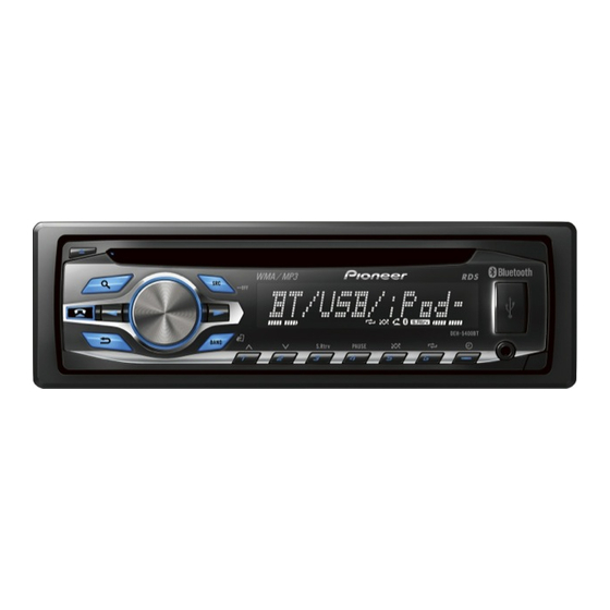
CD RDS RECEIVER
DEH-64BT
DEH-6400BT
DEH-5400BT
DEH-4400BT
DEH-4450BT
DEH-4490BT
This service manual should be used together with the following manual(s):
Model No.
Order No.
CRT4759
CX-3287
PIONEER CORPORATION
PIONEER ELECTRONICS (USA) INC. P.O. Box 1760, Long Beach, CA 90801-1760, U.S.A.
PIONEER EUROPE NV Haven 1087, Keetberglaan 1, 9120 Melsele, Belgium
PIONEER ELECTRONICS ASIACENTRE PTE. LTD. 253 Alexandra Road, #04-01, Singapore 159936
PIONEER CORPORATION 2011
Mech. Module
S11.6STD
CD Mech. Module : Circuit Descriptions, Mech. Descriptions, Disassembly
1-1, Shin-ogura, Saiwai-ku, Kawasaki-shi, Kanagawa 212-0031, Japan
DEH-64BT/XNUC
/XNUC
/XNUC
/XNEW5
/XNES
/XNID
Remarks
ORDER NO.
CRT4746
/XNUC
K-ZZZ JULY 2011 Printed in Japan
Advertisement
Table of Contents

Related Manuals for Pioneer DEH-5400BT


Summary of Contents for Pioneer DEH-5400BT
- Page 1 PIONEER CORPORATION 1-1, Shin-ogura, Saiwai-ku, Kawasaki-shi, Kanagawa 212-0031, Japan PIONEER ELECTRONICS (USA) INC. P.O. Box 1760, Long Beach, CA 90801-1760, U.S.A. PIONEER EUROPE NV Haven 1087, Keetberglaan 1, 9120 Melsele, Belgium PIONEER ELECTRONICS ASIACENTRE PTE. LTD. 253 Alexandra Road, #04-01, Singapore 159936...
-
Page 2: Safety Information
SAFETY INFORMATION CAUTION This service manual is intended for qualified service technicians; it is not meant for the casual do-it-yourselfer. Qualified technicians have the necessary test equipment and tools, and have been trained to properly and safely repair complex products such as those covered by this manual. Improperly performed repairs can adversely affect the safety and reliability of the product and may void the warranty. - Page 3 Laser diode characteristics Wave length : 785 nm to 814 nm Maximum output : 1 190 µW(Emitting period : unlimited) Additional Laser Caution Transistors Q101 in PCB drive the laser diodes. When Q101 is shorted between their terminals, the laser diodes will radiate beam. If the top cover is removed with no disc loaded while such short-circuit is continued, the naked eyes may be exposed to the laser beam.
-
Page 4: Table Of Contents
CONTENTS SAFETY INFORMATION............................. 2 1. SERVICE PRECAUTIONS ..........................5 1.1 SERVICE PRECAUTIONS ........................5 1.2 NOTES ON SOLDERING .......................... 7 2. SPECIFICATIONS ............................8 2.1 SPECIFICATIONS ............................. 8 2.2 DISC/CONTENT FORMAT ........................10 3. BASIC ITEMS FOR SERVICE.........................11 3.1 CHECK POINTS AFTER SERVICING......................11 3.2 PCB LOCATIONS ............................ -
Page 5: Service Precautions
1. SERVICE PRECAUTIONS 1.1 SERVICE PRECAUTIONS 1. You should conform to the regulations governing the product (safety, radio and noise, and other regulations), and should keep the safety during servicing by following the safety instructions described in this manual. 2. Before disassembling the unit, be sure to turn off the power. Unplugging and plugging the connectors during power-on mode may damage the ICs inside the unit. - Page 6 8. Capacitor Bond Lock (UC, EW5) Acetate Tape (GYH1026) Please stick acetate tape along white line. Please confirm line hiding with acetate tape. * length of tape : 24 ± 4 mm 9. Capacitor Bond Lock (ID, ES, ES1) Silicon Glue (GEM1017) Place the capacitor in the center of the silk print, and confirm it does not touch to the connector.
-
Page 7: Notes On Soldering
1.2 NOTES ON SOLDERING For environmental protection, lead-free solder is used on the printed circuit boards mounted in this unit. Be sure to use lead-free solder and a soldering iron that can meet specifications for use with lead-free solders for repairs accompanied by reworking of soldering. -
Page 8: Specifications
2. SPECIFICATIONS 2.1 SPECIFICATIONS DEH-64BT/XNUC, DEH-6400BT/XNUC, DEH-5400BT/XNUC General Power source ....14.4 V DC (10.8 V to 15.1 V al- USB standard specification lowable) ........USB 2.0 full speed Grounding system ... Negative type Maximum current supply Maximum current consumption ........ - Page 9 DEH-4400BT/XNEW5 General WAV signal format ....Linear PCM & MS ADPCM Power source......14.4 V DC (10.8 V to 15.1 V (Non-compressed) allowable) Grounding system....Negative type USB standard specification Maximum current consumption ...........USB 2.0 full speed ...........10.0 A Maximum current supply ..1 A Backup current ....
-
Page 10: Disc/Content Format
DEH-4450BT/XNES, DEH-4490BT/XNID General Rated power source ..14.4 V DC USB standard specification (allowable voltage range: ........USB 2.0 full speed 12.0 V to 14.4 V DC) Maximum current supply Grounding system ... Negative type ........1 A Maximum current consumption USB Class ....... -
Page 11: Basic Items For Service
3. BASIC ITEMS FOR SERVICE 3.1 CHECK POINTS AFTER SERVICING To keep the product quality after servicing, please confirm following check points. r i f Confirm whether the customer complain has The customer complain must not be been solved. reappeared. If the customer complain occurs with the Display, audio and operations must be specific media, use it for the operation check. -
Page 12: Pcb Locations
3.2 PCB LOCATIONS CD Core Unit (S11.6STD) BT Unit Tuner Amp Unit Keyboard Unit (A,B) Keyboard Unit (C,D,E,F) A:DEH-64BT/XNUC B:DEH-6400BT/XNUC C:DEH-5400BT/XNUC D:DEH-4400BT/XNEW5 E:DEH-4450BT/XNES F:DEH-4490BT/XNID Unit Number : QWM3362(A) : QWM3300(B) : QWM3299(C) : QWM3298(D) : QWM3301(E) : QWM3302(F) Unit Name... -
Page 13: Jigs List
3.3 JIGS LIST - Jigs List Name Jig No. Remarks 16P FFC GGD1310 Tuner Amp Unit - CD Core Unit Test Disc TCD-782 Checking the grating L.P.F. Checking the grating (Two pieces) Acetate Tape GYH1026 Capacitor Bond Lock Silicon Glue GEM1017 Capacitor Bond Lock - Grease List... -
Page 14: Block Diagram
4. BLOCK DIAGRAM TUNER AMP UNIT JA401 ANTENNA FMMIXIN1 DACOUTL PINDIN LNAIN RF FRONT END IC IC231 IC401 PCM1753DBQ TDA7706 I2CSCL TUNSCL DACCS I2CSDA TUNSDA DACSCK RSTN TUNPCE1 DACLRCK LRCK DACDATA DATA RESET DACBDATA IC651 DACBSCK S-80827CNMC-B8M AUDIO_XOUT VOUTL FLASH ROM IC671 B :PEB009A8 ILMPW... - Page 15 :DEH-64BT/XNUC JA251 PRE OUTPUT :DEH-6400BT/XNUC :DEH-5400BT/XNUC RCAG Q251 :DEH-4400BT/XNEW5 753DBQ RCAG :DEH-4450BT/XNES ELECTRONIC VOLUME/ :DEH-4490BT/XNID SOURCE SELECTOR Q252 IC201 PML022A TUNL IN2_L POUT_L IN1_L VOUTL JA901 IN3_L B.UP AUXL IN4+_L ILM+B FLIn FRONT_L RLIn REAR_L DATA IC301 PAL007E Q871 MUTE...
- Page 16 Q1859 Q1864 Q1855 Q1860 Q1865 Q1851 D1851 D1852 D1853 D1854 CN1911 ILM+B ILM+B ILM+B ILM+B USB5V USB5V KEYBOARD UNIT (DEH-5400BT/XNUC,DEH-4400BT/XNEW5,DEH-4450BT/XNES,DEH-4490BT/XNID) JA1921 CN1821 AUXR 3 AUXL AUXL FRONT_AUX AUXG 1 S1826 SOURCE ROTARY COMMANDER S1827 S1842 ROT0 KDT3 ROT1 KST2 KDT1...
-
Page 17: Diagnosis
5. DIAGNOSIS 5.1 OPERATIONAL FLOWCHART Power ON Vcc = 1.2 V Pin 5 PVcc = 3.3 V Pin 1 BSENS Pin 141 BSENS = L ASENS Pin 143 ASENS = L DSENS Pin 140 DSENS = L Starts communication with Grille microcomputer. -
Page 18: Error Code List
5.2 ERROR CODE LIST ERROR CODES If a CD memory device is inoperable, or operation of such media is stopped by an error, the error mode is established and a cause of the error is displayed by an error code. Indication of error codes is intended to reduce the number of calls from customers and facilitate failure analysis and repair work in servicing. - Page 19 USB storage device/iPod Message Cause Action Message Cause Action Turn the plug Connect a USB NO DEVICE When plug and N/A USB The USB device play is off, no and play on. connected to is Mass Storage Connect a com- USB storage de- not supported Class compliant...
- Page 20 ERROR-23 USB storage de- USB storage de- above action, vice was not for- vice should be for- please contact matted with matted with your dealer or an FAT12, FAT16 or FAT12, FAT16 or authorized FAT32. FAT32. Pioneer Service Station. DEH-64BT/XNUC...
-
Page 21: Connector Function Description
5.3 CONNECTOR FUNCTION DESCRIPTION ANTENNA MICROPHONE WIRED FRONT INPUT REMOTE OUTPUT 15 13 11 9 7 5 3 1 CONTROL 16 14 12 10 8 6 4 2 REAR OUTPUT or SUBWOOFER OUTPUT 1 FL+ 9 NC 2 FR+ 10 NC 11 NC 3 FL- 12 NC... -
Page 22: Service Mode
6. SERVICE MODE 6.1 DISPLAY TEST MODE The information such as the system microcomputer version is checked. [How to enter Test mode] Press “ 1 ” and “ 3 ” keys simultaneously to start resetting. [Operation key] Operation key Processing Remarks Enter display test mode 1 + 3... -
Page 23: Cd Test Mode
6.2 CD TEST MODE - Flow Chart [Key] [4]+[6]->BUP+ACC ON [CD] or [SOURCE] Test Mode IN Source ON Contents Display [BAND] Power On RF AMP (T.Offset is adjusted) Gain switching 00 00 00 [BAND] [>] [<] Power Off Focus Close Focus Mode switching Tracking Servo CRG +... -
Page 24: Disassembly
7. DISASSEMBLY While the photograph shown is slightly different from this model in shape, the disassembly procedure is the same. Removing the Panel Assy (Fig.1) Remove the two hooks. Remove the two hooks and then remove the Panel Assy. Fig.1 Panel Assy Removing the CD Mechanism Module (Fig.2, 3, 4) Remove the screw. - Page 25 Removing the BT Unit and Tuner Amp Unit (Fig.5) BT Unit Disconnect the FFC. Straighten the tabs at three locations indicated and then remove the BT Unit. Remove the two screws. Remove the two screws. Straighten the tabs Fig.5 at two locations indicated and then remove the Tuner Amp Unit.
- Page 26 Disassembling the Panel Part (Fig.7, 8) 1. Remove the arm while bending the rib of the panel upward. Fig.7 2. Press the upside hook and the bottom side hook of the button at the same time, and pull out the button. Fig.8 Assembling the Panel Part (Fig.9, 10, 11) 1.
- Page 27 3. Fit the spring in the groove at the position shown in the figure. 4. Fit the boss on the lower side of the arm in the lower hole of the panel, and then warp the rib on the panel in the direction shown in the figure and fit the boss of the arm in the panel.
- Page 28 How to carry the mecha unit 1. Hold the designated points (shown with dashed lines) of the upper chassis and the front/rear bracket. 2. Be careful not to hold the solid line portions or the CRG mecha part or insert foreign substances, to prevent distortion. 3.
- Page 29 How to remove the PU unit 1. Create an empty-clamp state according to “How to create empty clamp state (motor drive)”. 2. Hook the feeding screw biasing spring to a tentative hooking portion (Fig 2b). Be careful not to get injured by the spring edge.
-
Page 30: Each Setting And Adjustment
8. EACH SETTING AND ADJUSTMENT 8.1 CD ADJUSTMENT 1) Cautions on adjustments 2) Test mode This mode is used to adjust the CD mechanism module. In this product the single voltage (3.3 V) is used for the regulator. The reference voltage is the REFO1 (1.65 V) To enter the test mode. -
Page 31: Checking The Grating After Changing The Pickup Unit
8.2 CHECKING THE GRATING AFTER CHANGING THE PICKUP UNIT Note : The grating angle of the PU unit cannot be adjusted after the PU unit is changed. The PU unit in the CD mechanism module is adjusted on the production line to match the CD mechanism module and is thus the best adjusted PU unit for the CD mechanism module. - Page 32 Grating waveform Ech -> Xch 20 mV/div, AC Fch -> Ych 20 mV/div, AC 0 degrees 30 degrees 45 degrees 60 degrees 75 degrees 90 degrees DEH-64BT/XNUC...
-
Page 33: Pcl Output Confirmation
8.3 PCL OUTPUT CONFIRMATION - PCL output With the TESTIN (22 pin) status of IC601 to be “H”, it is shifted to PCL Output Test mode after reset started. Check that square wave of 600.0 kHz is output from PCL (8 Pin) of IC601. If clock signal is out of this range, this resonator (X602) must be changed for a new one. -
Page 34: Exploded Views And Parts List
9. EXPLODED VIEWS AND PARTS LIST OTES : Parts marked by " * " are generally unavailable because they are not in our Master Spare Parts List. The > mark found on some component parts indicates the importance of the safety factor of the part. Therefore, when replacing, be sure to use parts of identical designation. - Page 35 * QRB3188 Finnish * QRB3189 Danish * QRB3190 Portuguese * QRB3191 Greek * QRB3192 Turkish All operation manuals are supplied in PDF files by the CD-ROM. Regarding the availability of paper manual, contact Pioneer Service representative in your region. DEH-64BT/XNUC...
-
Page 36: Exterior
9.2 EXTERIOR DEH-5400BT/XNUC DEH-4400BT/XNEW5 DEH-4450BT/XNES DEH-4490BT/XNID DEH-64BT/XNUC... - Page 37 See Contrast table (2) Holder QNC3036 Label See Contrast table (2) Heat Sink QNR3002 (2) CONTRAST TABLE DEH-64BT/XNUC, DEH-6400BT/XNUC, DEH-5400BT/XNUC, DEH-4400BT/XNEW5, DEH-4450BT/XNES and DEH-4490BT/XNID are constructed the same except for the following: DEH-64BT/ DEH-6400BT/ DEH-5400BT/ DEH-4400BT/ DEH-4450BT/ DEH-4490BT/ Mark No.
-
Page 38: Cd Mechanism Module
9.3 CD MECHANISM MODULE (A) : GEM1024 (B) : GEM1043 DEH-64BT/XNUC... - Page 39 CD MECHANISM MODULE SECTION PARTS LIST Mark No. Description Part No. Mark No. Description Part No. Damper CNW1198 ..Screw BSZ20P040FTC CNW1726 Screw(M2 x 4) CBA1835 Motor Unit(M2)(LOAD/CRG) CXC4026 Washer CBF1038 Screw Unit CXC8894 Spring CBH3010 Arm Assy CXE5027 Washer CBF1037 Spring CBH2855...
-
Page 40: Schematic Diagram
10. SCHEMATIC DIAGRAM 10.1 TUNER AMP UNIT (GUIDE PAGE) Note: When ordering service parts, be sure to refer to " EXPLODED VIEWS AND PARTS LIST" or "ELECTRICAL PARTS LIST". Large size CN701 SCH diagram C707 C408 C432 CCG1205 CN701 C421 100p 100p C708... - Page 41 2.2k KYDT ANTPW R808 2.2k ROT0 ANTPW A DEH-64BT/XNUC R810 2.2k ROT1 B DEH-6400BT/XNUC L851 IC801 C DEH-5400BT/XNUC R875,R877,R874,R872, Q874,R885,D875,D876, MOUNT R882 D DEH-4400BT/XNEW5 C871,D872,R873,R884, OUTY : The power supply is shown with the marked box. R876,Q871,Q872,R879, MOUNT E DEH-4450BT/XNES...
- Page 42 PRE OUTPUT 1000p/50 C259 C260 C321 C320 C261 C319 100p/50 100p/50 100p/50 100p/50 C318 C255 C256 C257 C258 1p/50 100p/25 100p/50 R255 R256 R257 R258 C315 C314 C317 u/16 RN1910 RN1910 Q251 Q252 R303 R304 CCG1192-A C351 R352 C334 C333 C332 C331 R334...
- Page 43 10p/50 C321 10p/50 C320 10p/50 C319 10p/50 C318 100p/2 C315 0.1u/16 C312 D301 CRG03 C927 1000p/50 C923 CCG1192-A 1000p/50 C926 C351 1000u/16 C922 0.1u/16 0.1u/16 LTC114EUB 4.7k Q953 C931 C921 1/10W R352 R951 CCG1201-A 4.7u R912 C920 1000p/50 C919 4.7k 220u/6.3 CRG03 C924...
- Page 44 C238 C237 TRST ASEBRK TRST CCG1192-A ASEBRKAK/ASEBRK PCM1753DBQ C233 R619 0.01u/16 VOUTR C232 9 AGND VOUTL AUDIO_X2 10 VCOM R618 AUDIO_X1 1000p/50 11 ZEROR/ZEROA 0.1u/10 PVCC6 12 ZEROL/NA C239 C620 DGND VSS7 0.1u/10 LRCK VCC4 except LRCK C619 10p/50 DATA AUDIO_XOUT DATA R617...
- Page 45 R620 R642 BTRX BTRX VSS4 C851 CKIO 0.1u/10 PVCC4 C621 4.7k BTTX BTTX R851 KYDT/TESTDI KYDT DPDT/TESTDO 8.2k DPDT R809 0.1u/10 C618 VCC3 VSS3 0.1u/10 220p/50 C811 PVCC3 C616 220p/50 C810 TESIN TESTIN 100k R615 MUTE MUTE DZ2S068C D811 /USBFLG 2.2k DZ2S068C D810...
-
Page 46: Keyboard Unit
GP1UXC14RK SEG14 REMOTE DGND R1804 R1803 R1805 DGND DGND RED Key 0.01u/ DGND GREEN Key BLUE Key V1801 CAW2017-A SEGMENT LCD A DEH-64BT/XNUC B DEH-6400BT/XNUC R1896 R1897 C DEH-5400BT/XNUC ILMGND D DEH-4400BT/XNEW5 E DEH-4450BT/XNES F DEH-4490BT/XNID D1851 D1852 D1853 DEH-64BT/XNUC... - Page 47 KEYBOARD UNIT REFERNECE AREA MAP (only A, B) GRILLE uCON & LCD :1801-1820 KEY MATRIX&CONNECTOR :1821-1850 :1851-1910 :1911-1920 :1921-1930 BAND S1837 S1838 SOURCE KYDT DPDT S1839 ROTARY DISP COMMANDER L1801 S1840 C1912 S1842 S1841 0.1u/16 CN1821 CKS6287 DGND DGND ILMGND ILMGND SWVDD CSD1168-A...
-
Page 48: Cd Core Unit (S11.6Std)
10.3 CD CORE UNIT (S11.6STD) PICKUP UNIT(P10.6) (SERVICE) CXX3556 V3R3 E:P5+P10 F:P1+P6 PUEN Q102 LTA123JUB Q101 R109 2.2k 2SA1577(QR) V+3A ATEST V+3A P5+P10 P1+P6 REFO VREF A.VDD1 C221 A.GND1 0.1u/10 C216 1800p/50 RFAGC AGCO C220 HOLOGRAM UNIT 0.1u/10 C219 AGCI 0.1u/10 FOCUS ACT C228... - Page 49 CD CORE UNIT (S11.6STD) C302 C303 1000p/50 1000p/50 PUEN C304 0.022u/16 C305 0.1u/10 R310 4.7k R311 4.7k R312 4.7k R313 4.7k TEMP TEMP R215 TH201 Q201 TESTIN Mask Flash ATEST R232 ADENA R281 ADENA R282 R291 R294 BSCK0 /WAIT A.VDD1 A.GND1 C216 R291...
-
Page 50: Keyboard Unit
SIZE SYMBOL V1801 RS1/10SR***J-T CAW2017 RS1/4SA***J-T SEGMENT LCD ILMGND C, E, F D1851-D1865 SMLE12BC7T(NP) SML-D12V8W(PQ) COLOR BLUE R1851 A DEH-64BT/XNUC R1852 R1853 B DEH-6400BT/XNUC R1854 C DEH-5400BT/XNUC R1855 R1869 D DEH-4400BT/XNEW5 R1870 R1856 E DEH-4450BT/XNES R1857 F DEH-4490BT/XNID R1858 DEH-64BT/XNUC... - Page 51 KEYBOARD UNIT (only C, D, E, F) KEY MATRIX RIGHT S1833 ILMGND JA1921 S1834 CKN1090 AUXR CN1821 AUXL AUXG C1921 C1922 LIST CKS6287 BAND DGND S1828 S1837 ILMGND AUX:+2.2 dBs SWVDD S1829 S1838 DGND ROT1 S1842 ILM+B S1830 ROT0 S1835 S1839 USBGND KYDT...
-
Page 52: Bt Unit
10.5 BT UNIT 1u/10 CN21 CKS6346 SPK1N SPK1P MIC_BIAS MIC1P 1V8_EN MIC1N BT1.8V BT1.8V BTAGND BOOTS RESET BT1.8V IC21 BT3.3V BT3.3V NJM2846DL3-18 3.3V DBG_Tx DBG_Rx BTAGND U1OUT U1IN BT MODULE CWX4123 DEH-64BT/XNUC... - Page 53 BT UNIT CN22 VKN1189 U1OUT U1IN NRST_CPU BTAGND MIC1P CN961 MIC1N BT3.3V IC22 S-1206B33-U3 3.3V DEH-64BT/XNUC...
-
Page 54: Waveforms
10.6 WAVEFORMS - CD CORE UNIT(S11.6STD) Note : 1. The encircled numbers denote measuring points in the circuit diagram. 2. Reference voltage REFO1(1.65 V) 1DSCSNS 1DSCSNS 5 V/div 500 ms/div 5 V/div 500 ms/div 3HOME 5CLCONT 5 V/div 5 V/div 4LOEJ 4LOEJ 5 V/div... - Page 55 fRFAGC fRFAGC gLRCK 1 V/div 2 ms/div 1 V/div 200 ms/div 2 V/div 10 us/div hBCLK 500 mV/div 1 V/div 2 V/div 9TIN 8CIN 500 mV/div 500 mV/div DOUT(DATA) 2 V/div 7SIN 2 V/div 32 Tracks Jump waveform Search operation(Outter to Inner) Digital Out waveform (Zoom of 100 Track Jump waveform) Ref.:...
-
Page 56: Pcb Connection Diagram
C503 R501 R504 C502 R503 R502 C514 C508 C506 R506 R505 IC501 D501 R507 L501 C509 CN22 CN701 A DEH-64BT/XNUC B DEH-6400BT/XNUC C DEH-5400BT/XNUC D DEH-4400BT/XNEW5 (A, B) CN1821 E DEH-4450BT/XNES F DEH-4490BT/XNID (C, D, E, F) CN1821 FRON DEH-64BT/XNUC... - Page 57 SIDE A CEK1286 POWER SUPPLY L901 Q751 C321 JA901 IC301 D751 C754 R754 C309 C320 R753 Q752 D954 C310 R353 Q351 C319 C318 C901 ANTENNA R304 R302 R301 JA401 R303 D902 D901 Q301 C206 R952 R951 D941 KN401 C927 Q951 Q953 L941 Q952...
- Page 58 TUNER AMP UNIT TESTIN DEH-64BT/XNUC...
- Page 59 SIDE B DEH-64BT/XNUC...
-
Page 60: Keyboard Unit
11.2 KEYBOARD UNIT KEYBOARD UNIT SIDE A (only A, B) A DEH-64BT/XNUC B DEH-6400BT/XNUC C DEH-5400BT/XNUC D DEH-4400BT/XNEW5 E DEH-4450BT/XNES F DEH-4490BT/XNID DEH-64BT/XNUC... - Page 61 C1857 C1805 C1804 R1851 R1887 R1892 R1889 C1851 R1888 R1893 R1894 R1863 R1862 R1895 R1876 R1875 Q1860 C1863 Q1855 C1855 R1861 Q1853 Q1863 Q1859 A DEH-64BT/XNUC B DEH-6400BT/XNUC Q1854 Q1864 Q1858 C DEH-5400BT/XNUC D DEH-4400BT/XNEW5 E DEH-4450BT/XNES F DEH-4490BT/XNID DEH-64BT/XNUC...
-
Page 62: Cd Core Unit (S11.6Std)
11.3 CD CORE UNIT (S11.6STD) CD CORE UNIT (S11.6STD) SIDE A PICKUP UNIT(P10.6)(SERVICE) R254 TH201 LOADING/CARRIAGE C235 CN101 MOTOR R246 R232 HOME C102 S901 C201 D101 CN702 R253 R245 C238 R706 C240 C710 C205 R297 C299 C707 C705 C220 R702 R701 SPINDLE MOTOR... - Page 63 CD CORE UNIT (S11.6STD) SIDE B C104 Q102 R108 Q101 C202 X201 R109 R294 C203 C239 C209 C225 C101 C110 C233 C111 R237 C224 C210 C223 R296 C211 Q201 R240 R282 R293 C204 R283 R281 C284 C222 IC201 C281 C218 R292 C301 C282...
-
Page 64: Keyboard Unit
(only C, D, E, F) C1864 D1864 D1865 C1865 D1863 C1863 C1862 D1862 C1858 D1858 D1857 C1857 D1866 D1855 C1855 C1852 D1852 C1859 D1859 A DEH-64BT/XNUC B DEH-6400BT/XNUC C1860 C1851 C DEH-5400BT/XNUC D1851 D1860 C1853 D DEH-4400BT/XNEW5 E DEH-4450BT/XNES C1861 F DEH-4490BT/XNID D1861 DEH-64BT/XNUC... - Page 65 R1867 R1857 VA1923 C1922 C1923 C1921 CN801 C1804 C1805 R1801 R1802 R1860 R1859 R1822 R1821 R1863 R1853 R1865 R1855 A DEH-64BT/XNUC R1862 R1852 R1851 B DEH-6400BT/XNUC R1861 C DEH-5400BT/XNUC R1866 R1856 D DEH-4400BT/XNEW5 R1869 R1870 E DEH-4450BT/XNES F DEH-4490BT/XNID DEH-64BT/XNUC...
-
Page 66: Bt Unit
11.5 BT UNIT BT UNIT SIDE A IC21 CN22 IC22 CN961 CN21 BT MODULE BT UNIT SIDE B DEH-64BT/XNUC... -
Page 67: Electrical Parts List
IC 301 (A, 91, 111) IC NJM2068V Circuit Symbol and No. Part No. Circuit Symbol and No. Part No. : QWM3298(D) A:DEH-64BT/XNUC : QWM3301(E) B:DEH-6400BT/XNUC : QWM3302(F) C:DEH-5400BT/XNUC Unit Name : Tuner Amp Unit D:DEH-4400BT/XNEW5 MISCELLANEOUS E:DEH-4450BT/XNES IC 201 (A,98,112) IC PML022A F:DEH-4490BT/XNID... - Page 68 Circuit Symbol and No. Part No. Circuit Symbol and No. Part No. D 602 (A,127,50) Diode RB751S-40 D 751 (A,138,134) Diode RKZ8.2KG(B2) R 201 (A,100,59) RAB4CQ102J D 801 (A,114,13) Diode DZ2S068C R 231 (A,147,56) RS1/16SS821J D 802 (A,117,12) Diode DZ2S068C R 232 (A,148,56) RS1/16SS821J...
- Page 69 Circuit Symbol and No. Part No. Circuit Symbol and No. Part No. R 604 (A,104,76) RAB4CQ473J R 812 (A,120,18) (A,B) RS1/10SR222J R 607 (A,104,70) RS1/16SS473J R 813 (A,105,14) (A,B) RS1/10SR222J R 608 (A,104,69) RS1/16SS473J R 814 (A,105,11) (C,D,E,F) RS1/10SR0R0J R 609 (A,132,66) RS1/16SS101J R 815...
- Page 70 Circuit Symbol and No. Part No. Circuit Symbol and No. Part No. C 217 (A,96,105) CKSRYB105K10 C 423 (A,136,95) CKSSYB103K16 C 424 (A,162,91) CKSSYB472K25 C 232 (A,144,52) CKSSYB103K16 C 425 (A,162,92) CKSSYB472K25 C 233 (A,149,54) 10 uF CCG1192 C 234 (A,145,63) 10 uF CCG1192 C 426...
- Page 71 Circuit Symbol and No. Part No. Circuit Symbol and No. Part No. Q 1859 (B,21,23) Transistor LSC4081UB C 632 (A,115,47) CCSSCH120J50 Q 1860 (B,60,28) Transistor LSC4081UB C 633 (A,113,47) CCSSCH120J50 Q 1861 (B,53,16) Transistor LSC4081UB C 638 (A,122,43) CKSRYB105K10 Q 1862 (B,48,27) Transistor LSC4081UB C 651...
- Page 72 Circuit Symbol and No. Part No. Circuit Symbol and No. Part No. R 1884 (B,24,23) RS1/16SS101J R 215 (B,17,28) RS1/16SS393J R 1885 (B,18,26) RS1/16SS181J R 216 (B,12,35) RS1/16SS122J R 1886 (B,18,25) RS1/16SS181J R 217 (B,10,32) RS1/16SS562J R 1887 (B,70,22) RS1/16SS101J R 218 (B,10,35) RS1/16SS472J...
- Page 73 Circuit Symbol and No. Part No. Circuit Symbol and No. Part No. C 228 (B,10,33) CCSSCH270J50 CN1911 (A,155,22) Connector CKS6267 JA1921 (A,154,8) Jack CKN1090 C 229 (B,9,40) CKSSYB104K10 V 1801 (A,106,23) Segment LCD CAW2017 C 233 (B,32,46) CKSSYB103K16 RESISTORS C 236 (B,8,40) CKSSYB104K10 C 238...
- Page 74 Circuit Symbol and No. Part No. C 26 (A,33,38) 10 uF CCG1192 C 28 (A,23,49) CEVW470M6R3 C 29 (A,28,51) CKSRYB105K10 C 31 (A,35,46) CKSRYB103K50 C 33 (A,22,54) 10 uF CCG1192 C 34 (A,42,27) CKSRYB105K10 C 36 (A,35,49) CKSRYB104K16 Miscellaneous Parts List Pickup Unit(P10.6)(Service) CXX3556 Motor Unit(SPINDLE)