Table of Contents
Advertisement
SERVICE MANUAL
Ver 1.1 2002.08
Sony Corporation
9-873-618-02
2002H0500-1
e Vehicle Company
C 2002.08
Published by Sony Engineering Corporation
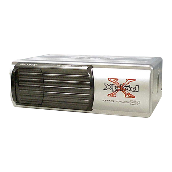
CDX-757MX
SPECIFICATIONS
System
Compact disc digital audio system
Laser diode properties Material: GaAlAs
Wavelength: 780 nm
Emission Duration: Continuous
Laser out-put Power: Less than
44.6 µW*
* This output is the value measured at a distance of 200 mm
from the objective lens surface on the Optical Pick-up Block.
Frequency response
5 – 20,000 Hz
Wow and flutter
Below the measurable limit
Signal-to-noise ratio
102 dB
Outputs
BUS control output (8 pins)
Analog audio output (RCA pin)
Current drain
800 mA (during CD playback)
800 mA (during loading or ejecting
a disc)
Operating temperature –10°C to +55°C (14°F to 131°F)
Approx. 262 × 90 × 185 mm
Dimensions
/8 × 3
/8 × 7
3
5
(10
(w/h/d) not incl. projecting parts
and controls
Mass
Approx. 2.1 kg (4 lb. 10 oz.)
Power requirement
12 V DC car battery
(negative ground)
Supplied accessories
Disc magazine (1)
Parts for installation and
connections (1 set)
Design and specifications are subject to change without
notice.
Canadian Model
Model Name Using Similar Mechanism
CD Drive Mechanism Type
Optical Pick-up Name
3
/8 in.)
COMPACT DISC CHANGER
US Model
E Model
CDX-747X
MG-251B-137
KSS-720A
Advertisement
Table of Contents

Related Manuals for Sony 757MX - Xplod CDX CD


Summary of Contents for Sony 757MX - Xplod CDX CD
- Page 1 (negative ground) Supplied accessories Disc magazine (1) Parts for installation and connections (1 set) Design and specifications are subject to change without notice. COMPACT DISC CHANGER Sony Corporation 9-873-618-02 2002H0500-1 e Vehicle Company C 2002.08 Published by Sony Engineering Corporation...
-
Page 2: Servicing Notes
SUR LES DIAGRAMMES SCHÉMATIQUES ET LA LISTE DES PIÈCES SONT CRITIQUES POUR LA SÉCURITÉ DE FONCTIONNEMENT. NE REMPLACER CES COM- POSANTS QUE PAR DES PIÈCES SONY DONT LES NUMÉROS SONT DONNÉS DANS CE MANUEL OU DANS LES SUPPLÉMENTS PUBLIÉS PAR SONY. - Page 3 CDX-757MX TEST DISC MP3 (MPEG 1 Audio Layer-3) is a standard technology and format for compressing a sound sequence. The file is compressed to about 1/10 of its This set can playback a CD-R, CD-RW for audio use. When test original size.
- Page 4 CDX-757MX Can the unit play a data CD with Q14 Is a file name/a folder name of FAQ- about MP3 Audio File folder levels? MP3 different from the name when creating a data CD (the The unit can play a data CD with folder What is MP3? levels.
-
Page 5: Table Of Contents
CDX-757MX TABLE OF CONTENTS SERVICING NOTES ............2 GENERAL Installation ............... 6 Connections ..............7 DISASSEMBLY 2-1. Disassembly Flow ............8 2-2. Case (Upper. T), Front Panel Assy ......... 9 2-3. Mechanism Deck (MG-251B-137) ......... 9 2-4. JACK Board ..............10 2-5. -
Page 6: General
CDX-757MX SECTION 1 This section is extracted from instruction manual. GENERAL Installation Installation Precautions Précautions • Choose the mounting location carefully, observing the following: • Choisir l’emplacement de montage en tenant compte des — The unit is not subject to temperatures exceeding 55°C (131°F) observations suivantes : (such as in a car parked in direct sunlight). -
Page 7: Connections
Connections/Connexions Connection diagram/Schéma de connexion For details, refer to the Installation/Connections manual of the car audio. Pour plus de détails, consulter le manuel d’installation/connexions de Sony BUS compatible car audio l’autoradio. Autoradio compatible BUS Sony BUS AUDIO IN BUS CONTROL IN Note For connecting two or more changers, the XA-C30 source selector (optional) is necessary. -
Page 8: Disassembly
CDX-757MX SECTION 2 DISASSEMBLY • This set can be disassembled in the order shown below. 2-1. DISASSEMBLY FLOW Note 1: The process described in can be performed in any order. Note 2: Without completing the process described in , the next process can not be performed. 2-2. -
Page 9: Case (Upper. T), Front Panel Assy
CDX-757MX Note: Follow the disassembly procedure in the numerical order given. 2-2. CASE (UPPER. T), FRONT PANEL ASSY 3 screw (PTT2.6 × 6) 3 screw (PTT2.6 × 6) 4 lever (FLT. 838) 5 case (upper. T) 1 screw (PTT2.6 × 6) 3 screw (PTT2.6 ×... -
Page 10: Jack Board
CDX-757MX 2-4. JACK BOARD Remove the jack board of the arrow. 1 ground point screw (PTT2.6 × 6) 2 jack board 2-5. MAIN BOARD, SLIDE VARIABLE RESISTOR (ELEVATOR HEIGHT SENSOR) (RV202) 1 main flexible board (CNJ101) 5 two screws (FP) 5 screw (FP) 6 main board 2 Remove two solders of... -
Page 11: Elj Motor Assy (Elevator) (M104)
CDX-757MX 2-6. ELJ MOTOR ASSY (ELEVATOR) (M104) 1 screw (PTT2 × 4) 2 bracket (EVM.S) 3 ELJ motor assy (elevator) (M104) 2-7. ESCUTCHEON (T) 3 two claws 2 Remove the claw in the direction of arrow A . 4 Remove the ditch in the direction of arrow B . -
Page 12: Chassis (U.s) Sub Assy
CDX-757MX 2-8. CHASSIS (U.S) SUB ASSY 2 Remove the edge in the direction 1 three screws of arrow A . (PTT2 × 4) 1 two screws (PTT2 × 4) 5 chassis (U.S) sub assy 1 screw (PTT2 × 4) 4 spring (SUT) 2-9. -
Page 13: Rf Board
CDX-757MX 2-10. RF BOARD 3 two screws (PS2 × 4) 4 RF board 3 two screws (PS2 × 4) 2 Remove four solders of the LSW board leads and spindle motor leads (M102). 2 Remove two solders of the sled motor leads 1 OP flexible board (CN102). -
Page 14: Lsw Board, Spindle Motor (S) Sub Assy (M102)
CDX-757MX 2-12. LSW BOARD, SPINDLE MOTOR (S) SUB ASSY (M102) 8 two precision screws (P1.7 × 2.2) 3 spring (chucking) 6 retainer (disc) 1 precision screw 4 precision screw (P2 × 2.5) (P2 × 2.2) 5 bracket (CP) 2 LSW board 9 Remove the spindle motor (S) sub assy (M102) in the direction of the arrow. -
Page 15: Assembly
CDX-757MX SECTION 3 ASSEMBLY • This set can be assembled in the order shown below. 3-1. ASSEMBLY FLOW 3-2. OPTICAL PICK-UP COMPLETE ASSY (Page 15) 3-3. GEAR (LOMINI) / (LOAD 1) ASSY (Page 16) 3-4. OPERATION CHECK (Page 16) 3-2. OPTICAL PICK-UP COMPLETE ASSY 1 Move the lever (LOCK 3A) in the direction of arrow A , and return it a little in the direction of arrow B... -
Page 16: Gear (Lomini)/(Load 1) Assy
CDX-757MX 3-3. GEAR (LOMINI)/(LOAD 1) ASSY gear (LOAD 2) 2 Attach the gear (LOMINI) at the position shown in Fig. A. gear (LOMINI) shaft (rotary prevention C) chuck plate 1 Move the lever (LOCK 3A) fully in the direction of arrow B to move the chuck plate up. -
Page 17: Mechanical Adjustment
CDX-757MX SECTION 4 MECHANICAL ADJUSTMENT • Elevator Height (Address) Adjustment Adjustment Method: Note: This adjustments is necessary when the system controller (IC201), variable resistor (RV201), slider (R), slider (L), or chassis (ELV) 1. Connect this set to the master unit (e.g. MDX-C7970), load a was replaced for any repair. -
Page 18: Electrical Check
Connection: 3. Be sure to use the disc “YEDS-18” parts code: 3-702-101-01, but only – RF Board (Component Side) – when indicated. 4. Use a master unit that supports SONY bus system. Connection: power supply (DC 14.4 V) master unit... - Page 19 CDX-757MX TRACKING OFFSET CHECK Connection: – RF Board (Component Side) – oscilloscope (DC range) TP (VC) – IC101 TP (TE) Procedure: 1. Connect the oscilloscope to TP (TE) and TP (VC) on the RF board. 2. Put the set into play mode by loading the disc (YEDS-18). 3.
-
Page 20: Diagrams
CDX-757MX SECTION 6 DIAGRAMS 6-1. BLOCK DIAGRAM – SERVO Section – DIGITAL SIGNAL PROCESSOR, FILTER DIGITAL SERVO PROCESSOR, DIGITAL DOUT D-RAM CONTROLLER 15 85 IC101 66 69 68 67 RF AMP, PCMDI 15 89 (Page 21) FOCUS/TRACKING ERROR AMP IC101 PCMD 15 88 RFAC... -
Page 21: Block Diagram - Main Section (1/2)
CDX-757MX 6-2. BLOCK DIAGRAM – MAIN Section (1/2) – SIGNAL PATH : CD PLAY DATA SERIAL VOUTL INPUT LRCK INTERFACE 8 TIME OVER SAMPLING ENHANCED OUTPUT AMP CN901 (1/2) LOW-PASS VCOM DIGITAL FILTER MULTI-LEVEL FILTER AUDIO OUT WITH DELATA-SIGMA CONVERTER LOW-PASS IC401 FUNCTION... -
Page 22: Block Diagram - Main Section (2/2)
IC305 CDON 29 CN901 (2/2) RESET SIGNAL GENERATOR CONTROL IC303 PS901 +3.3V BUS INTERFACE B. UP +3.3V REGULATOR B. UP (FOR SONY BUS) Q303, 304 IC302 DATA DATA EXTAL SCLK X201 12.288MHz BUSON OUT 63 XTAL BUSON BUSON OUT BUSON IN... -
Page 23: Note For Printed Wiring Boards And Schematic Diagrams
CDX-757MX 6-4. NOTE FOR PRINTED WIRING BOARDS AND SCHEMATIC DIAGRAMS • Circuit Boards Location Note on Printed Wiring Board: Note on Schematic Diagram: • X : parts extracted from the component side. • All capacitors are in µF unless otherwise noted. pF: µµF •... -
Page 24: Printed Wiring Boards - Rf/Lsw Boards
CDX-757MX 6-5. PRINTED WIRING BOARDS – RF/LSW Boards – • See page 23 for Circuit Boards Location. • Semiconductor Location Ref. No. Location IC101 IC201 Q101 Q102 M101 (SLED) M103 (CHUKING) OPTICAL PICK-UP BLOCK (KSS-720A) OP FLEXIBLE BOARD (RFAC) (VC) (TE) MAIN FLEXIBLE BOARD... -
Page 25: Schematic Diagram - Rf/Lsw Boards
CDX-757MX 6-6. SCHEMATIC DIAGRAM – RF/LSW Boards – • • See page 31 for for Waveforms. See page 34 for IC Block Diagrams. Q101 MSB709 -RT1 Q102 MUN2212T1 MAIN BOARD CN101 (1/3) (Page 28) The components identified by mark 0 or dotted Les composants identifiés par une marque 0 sont line with mark 0 are critical for safety. -
Page 26: Printed Wiring Boards - Main Board (Component Side)
CDX-757MX 6-7. PRINTED WIRING BOARDS – MAIN Board (Component Side) – • See page 23 for Circuit Boards Location. • Semiconductor Location MAIN BOARD (COMPONENT SIDE) Ref. No. Location D201 D301 IC306 D302 D303 D306 D310 IC605 IC101 IC501 IC102 IC201 IC202 F-11... -
Page 27: Printed Wiring Boards - Main (Conductor Side)/Switch Boards
CDX-757MX 6-8. PRINTED WIRING BOARDS – MAIN (Conductor Side)/SWITCH Boards – • See page 23 for Circuit Boards Location. • Semiconductor Location MAIN BOARD (CONDUCTOR SIDE) Ref. No. Location IC304 H-12 IC305 E-12 (CHASSIS) BP121 BP122 IC305 BP201 BP301 BP302 TP303 TP304 TP302... -
Page 28: Schematic Diagram - Main Board (1/3)
CDX-757MX 6-9. SCHEMATIC DIAGRAM – MAIN Board (1/3) – • • See page 31 for for Waveforms. See page 34 for IC Block Diagram. (1/3) R116 C114 IC102 GM71VS17403CLT-6 XCAS XRAS XCAS XRAS CN101 TP101 C101 D-RAM TP102 TP103 SRDR SRDR TP104 SFDR... -
Page 29: Schematic Diagram - Main (2/3)/Switch Boards
-TE85R DATA R115 R301 VREF (CHASSIS) BUSON BUSON BUSON BUSON RB604 100k ELEVATOR MOTOR DRIVE C301 C302 C303 BUS INTERFACE (FOR SONY BUS) GATE SWITCH IC604 TC7SH08FU -TE85R Q302 Q303 DTA115EKA-T146 2SB1184-TLR (CHASSIS) CN301 BUCHK RB603 RB602 S-RAM TP305 100k... -
Page 30: Schematic Diagram - Main Board (3/3)
CDX-757MX 6-11. SCHEMATIC DIAGRAM – MAIN Board (3/3) – • • See page 31 for for Waveforms. See page 34 for IC Block Diagram. (Page 28) (3/3) R501 D201 M1MA152WK-T1 R202 C201 100k XRDE DIGITAL FILTER, D/A CONVERTER C501 IC501 PCM1748E/2K DATA DATA... - Page 31 CDX-757MX • Waveforms – MAIN Board – – RF Board – 1 IC101 qh (FE) 1 IC101 rd (MDP) 6 IC601 qf (LRCKIA) qa IC501 qh (SCK) 2 Vp-p Approx. 4.5 Vp-p 100 mVp-p 5 Vp-p 3.8 µ s 22.7 µ s 59.1 ns 2 IC101 qk (TE) 2 IC101 ih (LRCK), ij (LRCKI)
-
Page 32: Printed Wiring Boards - Jack Board
6-12. PRINTED WIRING BOARDS – JACK Board – • See page 23 for Circuit Boards Location. JACK BOARD (COMPONENT SIDE) JACK BOARD (CONDUCTOR SIDE) CONTROL (FOR SONY BUS) (11) JACK FLEXIBLE BOARD CN901 MAIN BOARD CN301 (Page 26) AUDIO OUT... -
Page 33: Schematic Diagram - Jack Board
6-13. SCHEMATIC DIAGRAM – JACK Board – CNJ901 B.UP TP901 JACK TP902 FLEXIBLE DATA DATA TP903 CONTROL BOARD BUSON BUSON TP904 (FOR SONY BUS) TP905 CN901 SIRCS PS901 B.UP TP906 AUDIO OUT D901 B.UP STZ6.8N C901 C902 C904 -T146 0.001 100p B.UP... - Page 34 CDX-757MX • IC Block Diagrams – RF Board – IC101 CXA2581N-T4 RW/ROM DC OFST RFDCI – – RFDCO – RW/ROM VOFST APC AMP EQ ON/OFF RFAC EQ IN RW/ROM RFAC AC SUM SUMMING VOFST – – RW/ROM TE BAL RW/ROM –...
- Page 35 CDX-757MX IC201 LA6576L-TE-L S-GND THERMAL SHUT DOWN CH2-4 INPUT MUTE2 MUTE VCC2 MUTE1 MUTE VLO– OUTPUT VIN4 CONTROL VLO+ VIN4– – – VO4+ VIN4+ LEVEL – SHIFT VO4– VREF-IN VIN1/VREF VIN1 (VREF)-SW SWITCH VO3+ LEVEL VREF-OUT (CH1) SHIFT 5VREG VO3– –...
- Page 36 CDX-757MX – MAIN Board – IC101 CXD3027R 120 119 118 117 116 115 114 113 112 111 110 109 108 107 106 105 104 103 102 101 100 99 98 97 96 95 94 93 92 91 ERROR CLOCK PCMD CORRECTOR GENERATOR SELECTOR...
- Page 37 CDX-757MX IC301 LB1930M-TLM BUFFER OUT1 MOTOR CONTROL DRIVE CIRCUIT CIRCUIT OUT2 BUFFER P-GND S-GND IC302 BA8272AFV-E2 RESET SWITCH IC501 PCM1748E/2K 15 14 ZERO DETECT SYSTEM FUNCTION CLOCK OUTPUT AMP AND CONTROL LOW-PASS FILTER MANAGER CONVERTER INTERFACE 8 TIME OVER SAMPLING ENHANCED DIGITAL FILTER MULTI-LEVEL...
- Page 38 CDX-757MX IC601 CXD9684R-004 16 CE AD10 SWITCH 15 AD5 ROUND & LIMIT 14 LRCKIA VDDT C-POINTER REGISTER GENERAL OUTPUT 13 BCKIA PORT ADDRESS Y-POINTER CALC. REGISTER 12 SDI0 2 SETS 11 AD4 X-POINTER REGISTER AUDIO 10 AD3 ERAM 2k WORD 9 SDO REGISTER X0 X1 X2...
-
Page 39: Ic Pin Function Description
CDX-757MX 6-14. IC PIN FUNCTION DESCRIPTION • MAIN BOARD IC201 HD6432238RWN21TEIV (SYSTEM CONTROLLER) Pin No. Pin Name Description TEST Test mode setting terminal “L”: test mode Not used DECXRST Reset signal output to the CD-ROM/MP3 decoder “L”: reset DECSTBY Standby mode control signal output to the CD-ROM/MP3 decoder “H”: standby Focus OK signal input from the DSP “L”: NG, “H”: OK Guard frame sync signal input from the DSP “L”: NG, “H”: OK... - Page 40 Sub system clock input terminal Not used (fixed at “L”) System reset signal input from the SONY bus interface and reset signal generator “L”: reset For several hundreds msec. after the power supply rises, “L” is input, then it changes to “H”...
-
Page 41: Exploded Views
CDX-757MX SECTION 7 EXPLODED VIEWS NOTE: • -XX and -X mean standardized parts, so they • Items marked “*” are not stocked since they The components identified by mark 0 or dotted line with mark may have some difference from the original are seldom required for routine service. -
Page 42: Mechanism Deck Section-1 (Mg-251B-137)
CDX-757MX 7-2. MECHANISM DECK SECTION-1 (MG-251B-137) mechanism deck section-3 mechanism deck section-2 Ref. No. Part No. Description Remark Ref. No. Part No. Description Remark X-3378-091-1 CHASSIS (U. S) SUB ASSY 3-011-997-01 SPRING (STOPPER. LOWER) 3-024-161-01 SPRING (SUT) 7-685-781-09 SCREW +PTT 2X4 (S) -
Page 43: Mechanism Deck Section-2 (Mg-251B-137)
CDX-757MX 7-3. MECHANISM DECK SECTION-2 (MG-251B-137) M104 Ref. No. Part No. Description Remark Ref. No. Part No. Description Remark 3-024-170-01 SPRING (SB), TENSION * 154 3-014-685-01 SPACER (MO) * 152 3-040-790-02 BRACKET (EVM. S) M104 A-3301-123-A ELJ MOTOR ASSY (ELEVATOR) X-3378-092-7 CHASSIS (D. -
Page 44: Mechanism Deck Section-3 (Mg-251B-137)
CDX-757MX 7-4. MECHANISM DECK SECTION-3 (MG-251B-137) mechanism deck section-4 M103 Ref. No. Part No. Description Remark Ref. No. Part No. Description Remark * 201 3-024-150-01 RETAINER (CHM) * 211 A-3290-194-M MAIN ASSY, CHASSIS (EVY) * 202 X-3378-080-1 BRACKET (CHM. D) ASSY 3-010-254-11 SHAFT (ROTARY PREVENTION C) 3-321-813-01 WASHER, COTTER POLYETHYLENE 3-010-253-01 GEAR (LOMINI) -
Page 45: Mechanism Deck Section-4 (Mg-251B-137)
CDX-757MX 7-5. MECHANISM DECK SECTION-4 (MG-251B-137) not supplied not supplied M102 not supplied M101 not supplied The components identified by Les composants identifiés par une mark 0 or dotted line with marque 0 sont critiques pour la mark 0 are critical for safety. sécurité. -
Page 46: Electrical Parts List
CDX-757MX SECTION 8 ELECTRICAL PARTS LIST JACK MAIN NOTE: • Due to standardization, replacements in the • Items marked “*” are not stocked since they The components identified by 0 or dotted line with mark mark parts list may be different from the parts speci- are seldom required for routine service. - Page 47 CDX-757MX MAIN Ref. No. Part No. Description Remark Ref. No. Part No. Description Remark < TRANSISTOR > C407 1-115-651-11 ELECT 100uF C408 1-164-156-11 CERAMIC CHIP 0.1uF Q202 8-729-421-22 TRANSISTOR MUN2211T1 C409 1-115-650-11 ELECT 47uF Q301 8-729-010-25 TRANSISTOR MSD601-RT1 C410 1-115-650-11 ELECT 47uF Q302 8-729-028-62 TRANSISTOR...
- Page 48 CDX-757MX MAIN Ref. No. Part No. Description Remark Ref. No. Part No. Description Remark R411 1-216-847-11 METAL CHIP 150K 1/10W C209 1-164-227-11 CERAMIC CHIP 0.022uF R412 1-216-847-11 METAL CHIP 150K 1/10W C217 1-164-156-11 CERAMIC CHIP 0.1uF R413 1-216-809-11 METAL CHIP 1/10W R414 1-216-809-11 METAL CHIP...
- Page 49 CDX-757MX SWITCH Ref. No. Part No. Description Remark Ref. No. Part No. Description Remark < SWITCH > 1-529-566-31 SWITCH, PUSH (1 KEY) (CHUCKING END DETECT) 1-529-566-31 SWITCH, PUSH (1 KEY) (SAVE END DETECT) ************************************************************** 1-684-651-11 SWITCH BOARD ************* SW801 1-692-431-21 SWITCH, TACTILE (Z) ************************************************************** MISCELLANEOUS **************...
- Page 50 CDX-757MX US Model Canadian Model SERVICE MANUAL E Model Ver 1.1 2002.08 SUPPLEMENT-1 File this supplement with the service manual. Subject: Change of MAIN/SWITCH/JACK boards. (Suffix-12) (ECN-CSA06141) In this set, MAIN, SWITCH and JACK boards have been changed in the midway of production. Printed wiring boards and schematic diagrams of new type, and changed parts list are described in this supplement-1.
- Page 51 CDX-757MX • DIAGRAMS NOTE FOR PRINTED WIRING BOARDS AND SCHEMATIC DIAGRAMS Note on Printed Wiring Board: Note on Schematic Diagram: • X : parts extracted from the component side. • All capacitors are in µF unless otherwise noted. pF: µµF •...
- Page 52 CDX-757MX SCHEMATIC DIAGRAM – MAIN Board (1/3) – (1/3) R116 C114 IC102 GM71VS17403CLT-6 XCAS XRAS XCAS XRAS CN101 TP101 C101 D-RAM TP102 TP103 SRDR SRDR TP104 SFDR TP105 SFDR DIGITAL SIGNAL PROCESSOR, C162 TRDR TRDR SFDR DIGITAL SERVO PROCESSOR, TP106 MAIN D-RAM CONTROLLER TFDR...
- Page 53 -TE85R DATA R115 R301 VREF (CHASSIS) BUSON BUSON BUSON BUSON RB604 100k ELEVATOR MOTOR DRIVE C301 C302 C303 BUS INTERFACE (FOR SONY BUS) GATE SWITCH IC604 TC7SH08FU -TE85R Q302 Q303 (CHASSIS) DTA115EKA-T146 2SB1184-TLR CN301 BUCHK RB603 RB602 S-RAM TP305 100k...
- Page 54 CDX-757MX SCHEMATIC DIAGRAM – MAIN Board (3/3) – (Page 3) (3/3) D201 M1MA152WK-T1 R501 R202 C201 100k XRDE DIGITAL FILTER, D/A CONVERTER C501 IC501 PCM1748E/2K DATA DATA C502 LRCK LRCK DGND ZEROL ZEROR VOUTL MUTE VCOM MUTE LIM_SW VOUTR AGND SAVE R213 SAVE_SW...
- Page 55 CDX-757MX PRINTED WIRING BOARDS – MAIN Board (Component Side) – • Semiconductor Location MAIN BOARD (COMPONENT SIDE) Ref. No. Location D201 D202 IC306 D301 D302 D303 D306 IC605 D310 IC501 IC101 IC102 IC201 IC202 F-11 IC301 IC101 IC302 IC303 IC306 IC401 IC501 IC401...
- Page 56 CDX-757MX PRINTED WIRING BOARDS – MAIN (Conductor Side)/SWITCH Boards – • Semiconductor Location MAIN BOARD (CONDUCTOR SIDE) Ref. No. Location IC304 H-12 IC305 E-12 (CHASSIS) BP121 BP122 IC305 BP201 BP301 BP302 TP303 TP304 TP302 TP301 IC304 1-684-649- (12) (CHASSIS) M104 (ELEVATOR) SWITCH BOARD RV202...
- Page 57 CDX-757MX PRINTED WIRING BOARDS – JACK Board – JACK BOARD (COMPONENT SIDE) JACK BOARD (CONDUCTOR SIDE) CONTROL (FOR SONY BUS) (12) JACK FLEXIBLE BOARD CN901 MAIN BOARD CN301 (Page 6) AUDIO OUT (12) 1-684-650- SCHEMATIC DIAGRAM – JACK Board –...
- Page 58 CDX-757MX • EXPLODED VIEWS NOTE: • -XX and -X mean standardized parts, so they • Items marked “*” are not stocked since they may have some difference from the original are seldom required for routine service. Some one. delay should be anticipated when ordering •...
- Page 59 CDX-757MX JACK MAIN • ELECTRICAL PARTS LIST NOTE: When indicating parts by reference • Due to standardization, replacements in the • Items marked “*” are not stocked since they number, please include the board. parts list may be different from the parts speci- are seldom required for routine service.
- Page 60 CDX-757MX MAIN Ref. No. Part No. Description Remark Ref. No. Part No. Description Remark C501 1-164-156-11 CERAMIC CHIP 0.1uF C502 1-115-650-11 ELECT 47uF Q402 8-729-424-08 TRANSISTOR MUN2111T1 C503 1-164-156-11 CERAMIC CHIP 0.1uF Q410 8-729-920-21 TRANSISTOR DTC314TK-T-146 C504 1-115-650-11 ELECT 47uF Q420 8-729-920-21 TRANSISTOR DTC314TK-T-146...
- Page 61 CDX-757MX MAIN SWITCH Ref. No. Part No. Description Remark Ref. No. Part No. Description Remark R416 1-216-845-11 METAL CHIP 100K 1/10W R501 1-216-813-11 METAL CHIP 1/10W R601 1-216-821-11 METAL CHIP 1/10W R602 1-216-845-11 METAL CHIP 100K 1/10W R603 1-216-809-11 METAL CHIP 1/10W R607 1-216-814-11 METAL CHIP...
- Page 62 CDX-757MX MEMO...
-
Page 63: Revision History
CDX-757MX REVISION HISTORY Clicking the version allows you to jump to the revised page. Also, clicking the version at the upper right on the revised page allows you to jump to the next revised page. Ver. Date Description of Revision 2002.03 2002.08 Change of MAIN/SWITCH/JACK boards (Suffix-12)