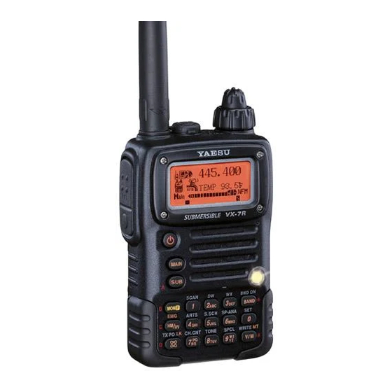
Yaesu VX-7R - TECHNICAL Service Manual
50/144/430 mhz triple-band heavy duty submersible transceiver
Hide thumbs
Also See for VX-7R - TECHNICAL:
- Operating manual (104 pages) ,
- Service manual (64 pages) ,
- Brochure & specs (4 pages)
Advertisement
50/144/430 MHz Triple-Band
Heavy Duty Submersible Transceiver
VX-7R
Technical Supplement
©2002 VERTEX STANDARD CO., LTD. Printed in Japan.
Specification .................................................................................................................................... 2
Exploded View & Miscellaneous Parts ........................................................................................ 4
Block Diagram ................................................................................................................................. 5
Interconnection Diagram ............................................................................................................... 6
Circuit Description ........................................................................................................................ 7
Alignment ...................................................................................................................................... 11
Board Unit (Schematics, Layouts & Parts)
RF Unit .................................................................................................................................................................... 19
AF Unit .................................................................................................................................................................... 33
CNTL Unit .............................................................................................................................................................. 43
VCO Unit ................................................................................................................................................................ 53
EH009M90A
Introduction
the VX-7R 50/144/430 MHzTriple-Band Heavy Duty Submersible Trans-
ceiver.
chip components. Attempts by non-qualified persons to service this
equipment may result in permanent damage not covered by the war-
ranty, and may be illegal in some countries.
this transceiver. Each side of the board is referred to by the type of the
majority of components installed on that side ("Side A" or "Side B"). In
most cases one side has only chip components, and the other has either
a mixture of both chip and leaded components (trimmers, coils, electro-
lytic capacitors, ICs, etc.), or leaded components only.
DW
TEX STANDARD assumes no liability for damage that may occur as a
result of typographical or other errors that may be present. Your coop-
eration in pointing out any inconsistencies in the technical information
would be appreciated.
Contents
VERTEX STANDARD CO., LTD.
4-8-8 Nakameguro, Meguro-Ku, Tokyo 153-8644, Japan
VERTEX STANDARD
US Headquarters
10900 Walker Street, Cypress, CA 90630, U.S.A.
International Division
8350 N.W. 52nd Terrace, Suite 201, Miami, FL 33166, U.S.A.
YAESU EUROPE B.V.
P.O. Box 75525, 1118 ZN Schiphol, The Netherlands
YAESU UK LTD.
Unit 12, Sun Valley Business Park, Winnall Close
Winchester, Hampshire, SO23 0LB, U.K.
VERTEX STANDARD HK LTD.
Unit 5, 20/F., Seaview Centre, 139-141 Hoi Bun Road,
Kwun Tong, Kowloon, Hong Kong
This manual provides the technical information necessary for servicing
Servicing this equipment requires expertise in handing surface-mount
Two PCB layout diagrams provided for each double-sided board in
While we believe the information in this manual to be correct, VER-
1
Advertisement
Table of Contents

Related Manuals for Yaesu VX-7R - TECHNICAL


Summary of Contents for Yaesu VX-7R - TECHNICAL
-
Page 1: Table Of Contents
10900 Walker Street, Cypress, CA 90630, U.S.A. VX-7R International Division 8350 N.W. 52nd Terrace, Suite 201, Miami, FL 33166, U.S.A. YAESU EUROPE B.V. P.O. Box 75525, 1118 ZN Schiphol, The Netherlands YAESU UK LTD. Technical Supplement Unit 12, Sun Valley Business Park, Winnall Close Winchester, Hampshire, SO23 0LB, U.K. -
Page 2: Specification
Specifications General Frequency Ranges: Rx (MAIN): 0.5 - 1.8 MHz (BC Band) 1.8 - 30 MHz (SW Band) 30-59 MHz (50 MHz HAM: USA version) 30-76 MHz (50 MHz HAM: EXP version) 59-108 MHz (FM: USA version) 76-108 MHz (FM: EXP version) 108-137 MHz (Air Band) 137-174 MHz (144 MHz HAM) 174-222 MHz (VHF-TV) -
Page 3: Specifications
Specifications Transmitter RF Power Output: 5/2.5/1.0/0.5 W (50/144/430 MHz, FM) 0.3 W (220 MHz, FM) 1.0 W (50 MHz, FM) Modulation Type: FM: Variable Reactance AM: Early Stage (Low Level) Maximum Deviation: ±5/±2.5 kHz Spurious Emission: At least 60 dB below (@ Tx 1W) Microphone Impedance: 2 k-ohm Receiver... -
Page 4: Exploded View & Miscellaneous Parts
Exploded View & Miscellaneous Parts No. VXSTD P/N DISCRIPTION QTY. À U9900137 BINDING HEAD SCREW M2X21.7 (W/ O RING) Â Á U9900138 BINDING HEAD SCREW M2X5 (W/ O RING) Â RA0417100 Â Â Â U07225120 PAN HEAD SCREW M2X2.5SUS#1 PANEL FRAME Ã... -
Page 5: Block Diagram
Block Diagram... -
Page 6: Interconnection Diagram
Interconnection Diagram... -
Page 7: Circuit Description
Circuit Description The VX-7R consists of a RF-UNIT, a CNTL-UNIT and filter characteristics are provided for each specific oper- an AF-UNIT. The RF-UNIT contains the receiver front ating frequency. end, PLL IC, power and switching circuits, and the VCO- (3) 435-MHz Band and 222-540MHz Reception UNIT for transmit and receive local signal oscillation. - Page 8 Circuit Description (5) 0.5 - 30 MHz Reception tal X1001 on the RF-UNIT is multiplied fourfold by Q2004 Received signals between 0.5 and 30 MHz pass through (2SC4915-0) and Q2012 (2SC4154E) to provide the 46.8- the Triplexer circuit, low-pass filter circuit, HF T/R switch MHz second local signal, applied to the Narrow IF IC.
- Page 9 Circuit Description it switches Q1048 (KRC654U) to disable the receiver cir- ered by amplifier Q4006 and Q1016 and delivered cuits. This causes the "red" mode of BUSY/TX lamp D3033 through UHF T/R diode switch D1045 to the RF-UNIT. to light. The modulated low-level UHF transmit signal from the VCO is passed through diode switch D1045 (HN2D01FU) (2) Modulation...
- Page 10 Circuit Description PLL Frequency Synthesizer a pulse corresponding to the phase difference between them. This pulse is fed to the charge pump, and the out- PLL IC Q1019 on the RF-UNIT consists of a data shift put from the charge pump passes through a loop filter register, reference frequency divider, phase comparator, composed of L1044, R1089, C1175, and either R1090, charge pump, "intermittent operation"...
-
Page 11: Alignment
Alignment Introduction and Precautions Required Test Equipment The VX-7R has been carefully aligned at the factory for RF Signal Generator with calibrated output level at 500 MHz the specified performance across the specified amateur Deviation Meter (linear detector) bands. Realignment should therefore not be necessary In-line Wattmeter with 5% accuracy at 500 MHz except in the event of a component failure. -
Page 12: Test Setup
Alignment Test Setup Squelch Preset Threshold (THLD SQL) [86] Set up the test equipment as shown below for transceiv- Inject a –15.0 dBµ RF signal (1 kHz tone @ ±3.5 kHz er alignment, and apply 8.7 V DC power to the transceiv- deviation), then press the V/M button, then press the er. - Page 13 Alignment L1 Tx Power Adjustment (L1 POWER) High TX Power Adjustment (L2 POWER) Transmit, and adjust the output power level for 50 mW Transmit, and adjust the output power level for 1.0 W (+50/-30 mW) by rotating the DIAL, then press the V/M (±0.1 W) by rotating the DIAL, then press the V/M but- button.
- Page 14 Alignment Squelch Preset Threshold (THLD SQL) L1 Tx Power Adjustment (L1 POWER) Inject a –15.0 dBµ RF signal (1 kHz tone @ ±3.5 kHz Transmit, and adjust the output power level for 50 mW deviation), then press the V/M button, then press the (+50/-30 mW) by rotating the DIAL, then press the V/M MON/F button twice.
- Page 15 Alignment High TX Power Adjustment (L3 POWER) Press the BAND button to activate the 145 MHz band Transmit, and adjust the output power level for 2.5 W internal alignment routine. (±0.2 W) by rotating the DIAL, then press the V/M but- The alignment frequency will automatically be set to ton.
- Page 16 Alignment High TX Power Adjustment (HI POWER) Press the MON/F to activate the TX Power and Devia- Transmit, and adjust the output power level for 5.0 W tion alignment routine. (±0.3 W) by rotating the DIAL, then press the V/M but- The alignment frequency will automatically be set to ton.
- Page 17 Alignment DCS Tx Deviation Adjustment (DCS DEV) DCS Tx Deviation Adjustment (DCS DEV) Press the V/M button, then transmit and adjust the de- Press the V/M button, then transmit and adjust the de- viation for 0.6 kHz (±0.1 kHz) by rotating the DIAL, viation for 0.6 kHz (±0.1 kHz) by rotating DIAL, then then press the V/M button.
- Page 18 Alignment Press the SUB button to activate the SUB band inter- Squelch Preset Tight (TIGH SQL) nal alignment routine. Adjust the generator level to –4.0 dBµ, then press the The alignment frequency will automatically be set to V/M button, then press the MON/F button twice. Press 435.100 MHz (USA Version: 440.100 MHz) on the SUB the V/M button, then rotate the DIAL to select the next band.
-
Page 19: Rf Unit
RF Unit Circuit Diagram MAIN NFM RX:+14.7dBµ (50M TX:1.84V) 435.000MHz, @12dB SINAD (144M TX:1.85V) 1000pF Coupling Capacitor. 800M RX:1.87V (430M TX:2.85V) 800M RX:0.8V 145M TX:+5.1dBm 800M RX:0.73V 800M RX:1.61V 13.5V 430M TX:+6.9dBm (13.3V) (1.86V) 1000pF Coupling Capacitor. (1.98V) (3.97V) MAIN NFM RX:+7.3dBµ 435.000MHz 1000pF Coupling Capacitor. - Page 20 RF Unit Parts Layout Side A Side B NJM12902V MB15A01PFV1 2SA1774 (FR) 2SK3475 KRC654U-RTK (Q1022) HN2D01FU (A1) 1SS321 (F9) (Q1019) UMW1 (W1) (Q1033, 1036, 1038, (Q1023) (Q1040, 1048, 1049) (D1045, 1046) (D1047) (Q1044) 1046, 1052) DAN222 (N) (D1006, 1007, 1008, 1009, 1010, 1011, 1012, 1027, 1028, 1041, 1043, 1044,...
-
Page 21: Parts List
RF Unit Parts List REF. DESCRIPTION VALUE TOL. MFR’S DESIG VXSTD P/N VERS. LOT. SIDE LAY ADR. PCB with Components (with VCO Unit) CB7372002 PCB with Components (with VCO Unit) EXPORT CB7372003 PCB with Components (with VCO Unit) GERMANY CB7372004 Printed Circuit Board FR008200C C 1001 CHIP CAP. - Page 22 RF Unit REF. DESCRIPTION VALUE TOL. MFR’S DESIG VXSTD P/N VERS. LOT. SIDE LAY ADR. C 1062 CHIP CAP. UMK105CH040CW-F K22178252 C 1063 CHIP CAP. UMK105CH040CW-F K22178252 C 1064 CHIP CAP. 0.001uF UMK105B102KW-F K22178829 C 1065 CHIP CAP. 0.001uF UMK105B102KW-F K22178829 C 1066 CHIP CAP.
- Page 23 RF Unit REF. DESCRIPTION VALUE TOL. MFR’S DESIG VXSTD P/N VERS. LOT. SIDE LAY ADR. C 1124 CHIP CAP. 56pF UMK105CH560JW-F K22178276 C 1125 CHIP CAP. 0.001uF UMK105B102KW-F K22178829 C 1126 CHIP CAP. UMK105CH060DW-F K22178254 C 1127 CHIP CAP. UMK105CK020CW-F K22178250 C 1128 CHIP CAP.
- Page 24 RF Unit REF. DESCRIPTION VALUE TOL. MFR’S DESIG VXSTD P/N VERS. LOT. SIDE LAY ADR. C 1200 CHIP CAP. 0.001uF UMK105B102KW-F K22178829 C 1201 CHIP CAP. 0.001uF UMK105B102KW-F K22178829 C 1202 CHIP CAP. GRM39F105Z10PT K22105001 C 1203 CHIP CAP. GRM39F105Z10PT K22105001 C 1205 CHIP CAP.
- Page 25 RF Unit REF. DESCRIPTION VALUE TOL. MFR’S DESIG VXSTD P/N VERS. LOT. SIDE LAY ADR. C 1258 CHIP CAP. 0.001uF UMK105B102KW-F K22178829 C 1259 CHIP CAP. UMK105CK020CW-F K22178250 C 1260 CHIP CAP. 0.001uF UMK105B102KW-F K22178829 C 1262 CHIP CAP. UMK105CK010CW-F K22178248 C 1264 CHIP CAP.
- Page 26 RF Unit REF. DESCRIPTION VALUE TOL. MFR’S DESIG VXSTD P/N VERS. LOT. SIDE LAY ADR. C 1323 CHIP CAP. 0.001uF UMK105B102KW-F K22178829 D 1001 DIODE 1SS362 TE85R G2070268 D 1002 DIODE 1SS362 TE85R G2070268 D 1003 DIODE 1SS362 TE85R G2070268 D 1004 DIODE 1SV271 TPH3 G2070476...
- Page 27 RF Unit REF. DESCRIPTION VALUE TOL. MFR’S DESIG VXSTD P/N VERS. LOT. SIDE LAY ADR. D 1061 DIODE RB751S-40TE61 G2070850 D 1062 DIODE 1SV271 TPH3 G2070476 D 1063 DIODE DAN222 TL G2070174 D 1064 DIODE 1SS400 TE61 G2070634 FB1001 CHIP COIL BLM21P300SPT L1690840 HS1001 HEATSINK PLATE...
- Page 28 RF Unit REF. DESCRIPTION VALUE TOL. MFR’S DESIG VXSTD P/N VERS. LOT. SIDE LAY ADR. L 1050 M.RFC 0.1uH C1608CA-R10G L1691045 L 1051 COIL E2 0.25-1.85-8.5T-L L0022576 L 1052 COIL E2 0.4-1.3-2T-L L0022580 L 1053 M.RFC 4.7uH LK1608 4R7K-T L1690688 L 1054 COIL E2 0.5-1.4-2.5T-L L0022750...
- Page 29 RF Unit REF. DESCRIPTION VALUE TOL. MFR’S DESIG VXSTD P/N VERS. LOT. SIDE LAY ADR. Q 1034 TRANSISTOR DTC144EE TL G3070075 Q 1035 TRANSISTOR DTC144EE TL G3070075 Q 1036 TRANSISTOR 2SA1774 TL R G3117748R Q 1037 TRANSISTOR KRA760U-RTK G3070278 Q 1038 TRANSISTOR 2SA1774 TL R G3117748R Q 1039 TRANSISTOR...
- Page 30 RF Unit REF. DESCRIPTION VALUE TOL. MFR’S DESIG VXSTD P/N VERS. LOT. SIDE LAY ADR. R 1043 CHIP RES. 100k 1/16W RMC1/16S 104JTH J24189049 R 1044 CHIP RES. 1/16W RMC1/16S 102JTH J24189025 R 1045 CHIP RES. 1/16W RMC1/16S 473JTH J24189045 R 1046 CHIP RES.
- Page 31 RF Unit REF. DESCRIPTION VALUE TOL. MFR’S DESIG VXSTD P/N VERS. LOT. SIDE LAY ADR. R 1098 CHIP RES. 1/16W RMC1/16S 101JTH J24189013 R 1099 CHIP RES. 1/16W RMC1/16S 103JTH J24189037 R 1100 CHIP RES. 1/16W RMC1/16S 331JTH J24189019 R 1102 CHIP RES. 3.3k 1/16W RMC1/16S 332JTH...
- Page 32 RF Unit Note:...
-
Page 33: Af Unit
AF Unit Circuit Diagram 2.2V (0V) BUSY:0.55V BUSY:9.2V 0V (0V) 2.3V (0V) WFM RX:2.94V 13.3V (13.1V) 0.4V (0.4V) 0V (0V) 2.85V BUSY:4.3V MAIN NFM RX:+4.6dBµ (0V) 0.4V (0.4V) @47.25MHz NFM:2.55V BUSY:3.0V 1000pF Coupling Capacitor. (0V) 0V (0V) 2.4V (0V) NFM:0.65V NFM:0.73V WFM RX:2.2V (0V) - Page 34 AF Unit Parts Layout Side A MB15A01PFV1 BU4094BCFV-E2 TA31136FN TDA7233D DTA144EE (16) DTC143ZE (E23) 2SJ364-R(4M) (Q2007) (Q2048) (Q2016, 2037) (Q2040) (Q2008, 2034) (Q2039) (Q2029, 2036, 2042, 2043, 2047) 2SC4154E (LE) UMB3N (B3) CPH6102 (AB) 2SA1774 (FR) 2SC5374 (NA) DTC144EE (26) (Q2003, 2012, 2022, (Q2003) (Q2033)
- Page 35 AF Unit Parts List REF. DESCRIPTION VALUE TOL. MFR’S DESIG VXSTD P/N VERS. LOT. SIDE LAY ADR. *** AF UNIT *** PCB with Components CB1870001 Printed Circuit Board FR008210C C 2001 CHIP CAP. 33pF UMK105CH330JW-F K22178270 C 2002 CHIP CAP. 0.01uF GRM36B103K16PT K22128804...
- Page 36 AF Unit REF. DESCRIPTION VALUE TOL. MFR’S DESIG VXSTD P/N VERS. LOT. SIDE LAY ADR. C 2067 CHIP CAP. 0.001uF UMK105B102KW-F K22178829 C 2068 CHIP CAP. 0.001uF UMK105B102KW-F K22178829 C 2069 CHIP CAP. 0.001uF UMK105B102KW-F K22178829 C 2070 CHIP CAP. 10pF UMK105CH100DW-F K22178258...
- Page 37 AF Unit REF. DESCRIPTION VALUE TOL. MFR’S DESIG VXSTD P/N VERS. LOT. SIDE LAY ADR. C 2129 CHIP CAP. 0.001uF UMK105B102KW-F K22178829 C 2130 CHIP CAP. 820pF GRM36B821K50PT K22178808 C 2131 CHIP TA.CAP. 4.7uF 6.3V TEMSVA20J475M-8R K78080031 C 2132 CHIP CAP. 0.01uF GRM36B103K16PT K22128804...
- Page 38 AF Unit REF. DESCRIPTION VALUE TOL. MFR’S DESIG VXSTD P/N VERS. LOT. SIDE LAY ADR. D 2004 DIODE DAN222 TL G2070174 D 2005 DIODE HVC355B(TAPE) G2070588 D 2006 DIODE 1SV325(TPH3) G2070848 D 2007 DIODE DAN222 TL G2070174 D 2008 DIODE DAN222 TL G2070174 D 2009 DIODE...
- Page 39 AF Unit REF. DESCRIPTION VALUE TOL. MFR’S DESIG VXSTD P/N VERS. LOT. SIDE LAY ADR. Q 2019 TRANSISTOR 2SC5374-TL G3353748 Q 2020 TRANSISTOR 2SA1774 TL R G3117748R Q 2021 TRANSISTOR 2SA1774 TL R G3117748R Q 2022 TRANSISTOR 2SC4154-T11-1E G3341548E Q 2023 TRANSISTOR 2SC4154-T11-1E G3341548E Q 2024 TRANSISTOR...
- Page 40 AF Unit REF. DESCRIPTION VALUE TOL. MFR’S DESIG VXSTD P/N VERS. LOT. SIDE LAY ADR. R 2034 CHIP RES. 4.7k 1/16W RMC1/16S 472JTH J24189033 R 2035 CHIP RES. 1/16W RMC1/16S 223JTH J24189041 R 2036 CHIP RES. 1/16W RMC1/16S 103JTH J24189037 R 2037 CHIP RES.
- Page 41 AF Unit REF. DESCRIPTION VALUE TOL. MFR’S DESIG VXSTD P/N VERS. LOT. SIDE LAY ADR. R 2097 CHIP RES. 330k 1/16W RMC1/16S 334JTH J24189055 R 2098 CHIP RES. 100k 1/16W RMC1/16S 104JTH J24189049 R 2099 CHIP RES. 1/16W RMC1/16S 221JTH J24189017 R 2100 CHIP RES.
- Page 42 AF Unit Note:...
-
Page 43: Cntl Unit
CNTL Unit Circuit Diagram 1.17V max~0.48V min 2.69V max~0.47V min 3.0V 0.47V (0.83V) 0V (0.87V) 0V (0.87V) 3.0V 1.83V max ~0.01V min 1.70V max 2.96V max 3.0V 11.3V max~12.0V min 13.1V 13.3V ~0.46V min ~0.80V min (13.2V) (12.9V) 1.12V max~0.11V min 3.0V (3.0V) 3.0V (3.0V) 0.8V (2.1V) - Page 44 CNTL Unit Parts Layout HD6472237TF10 M62364FP NJM12902V (Q3035) (Q3012) (Q3006, 3010, 3020) AT24C128N-10SI-2.7 NJM2904V NJM3403AV (Q3034) (Q3005, 3030) (Q3018) NJU7231F30 S-35L12AEFS-TB (Q3025) (Q3044) 2SJ364-R RH5RH651A CPH6102 (AB) NJU7007F2-TE1 (Q3016, 3021, 3022) (Q3028) (Q3039) (Q3017) KRX202U-RTK UMW1 (W1) 2SD1801S TAR5S30 (Q3024) (Q3029) (Q3041) (Q3040)
- Page 45 CNTL Unit Parts List REF. DESCRIPTION VALUE TOL. MFR’S DESIG VXSTD P/N VERS. LOT. SIDE LAY ADR. PCB with Components CB1871002 PCB with Components CB1871003 VERSION A1 PCB with Components CB1871004 VERSION A2 PCB with Components CB1871005 VERSION A3 PCB with Components CB1871006 VERSION B1 PCB with Components...
- Page 46 CNTL Unit REF. DESCRIPTION VALUE TOL. MFR’S DESIG VXSTD P/N VERS. LOT. SIDE LAY ADR. C 3046 CHIP CAP. GRM39F105Z10PT K22105001 C 3047 CHIP TA.CAP. 220uF SK4-0G227M-RD K78060014 C 3048 CHIP CAP. GRM39F105Z10PT K22105001 C 3049 CHIP CAP. 0.001uF UMK105B102KW-F K22178829 C 3050 CHIP CAP.
- Page 47 CNTL Unit REF. DESCRIPTION VALUE TOL. MFR’S DESIG VXSTD P/N VERS. LOT. SIDE LAY ADR. C 3126 CHIP CAP. GRM39F105Z10PT K22105001 C 3127 CHIP CAP. 0.001uF UMK105B102KW-F K22178829 C 3129 CHIP CAP. 0.001uF UMK105B102KW-F K22178829 C 3130 CHIP TA.CAP. 33uF TEMSVA0G336M-8R K78060036 C 3131 CHIP CAP.
- Page 48 CNTL Unit REF. DESCRIPTION VALUE TOL. MFR’S DESIG VXSTD P/N VERS. LOT. SIDE LAY ADR. Q 3007 TRANSISTOR DTC144EE TL G3070075 Q 3008 TRANSISTOR DTA144EE TL G3070074 Q 3009 TRANSISTOR 2SC4154-T11-1E G3341548E Q 3010 IC NJM12902V(TE1) G1093592 Q 3011 TRANSISTOR DTC144EE TL G3070075 Q 3012 IC...
- Page 49 CNTL Unit REF. DESCRIPTION VALUE TOL. MFR’S DESIG VXSTD P/N VERS. LOT. SIDE LAY ADR. R 3026 CHIP RES. 1/16W RMC1/16S 473JTH J24189045 R 3027 CHIP RES. 1/16W RMC1/16S 683JTH J24189047 R 3028 CHIP RES. 1/16W RMC1/16S 333JTH J24189043 R 3029 CHIP RES. 1/16W RMC1/16S 473JTH J24189045...
- Page 50 CNTL Unit REF. DESCRIPTION VALUE TOL. MFR’S DESIG VXSTD P/N VERS. LOT. SIDE LAY ADR. R 3087 CHIP RES. 1/16W RMC1/16S 473JTH J24189045 R 3088 CHIP RES. 100k 1/16W RMC1/16S 104JTH J24189049 R 3088 CHIP RES. 100k 1/16W 0.50% RR0510R-104-D J24189167 R 3089 CHIP RES.
- Page 51 CNTL Unit REF. DESCRIPTION VALUE TOL. MFR’S DESIG VXSTD P/N VERS. LOT. SIDE LAY ADR. R 3150 CHIP RES. 1/16W RMC1/16S 105JTH J24189061 R 3151 CHIP RES. 1/16W RMC1/16S 473JTH J24189045 R 3152 CHIP RES. 1/16W RMC1/16S 223JTH J24189041 R 3153 CHIP RES. 1/16W RMC1/16S 223JTH J24189041...
- Page 52 CNTL Unit Note:...
-
Page 53: Vco Unit
VCO Unit Circuit Diagram Parts Layout Side A Side B DTC143ZE (E23) EC3H07B (G) (Q4001, 4003, 4007) (Q4002, 4004, 4005, 4006) - Page 54 VCO Unit Note...
- Page 55 VCO Unit Parts List REF. DESCRIPTION VALUE TOL. MFR’S DESIG VXSTD P/N VERS. LOT. SIDE LAY ADR. PCB with Components CB1872001 Printed Circuit Board FR007830D C 4001 CHIP CAP. 0.001uF UMK105B102KW-F K22178829 C 4002 CHIP CAP. 0.01uF GRM36B103K16PT K22128804 C 4003 CHIP CAP. 0.5pF UMK105CK0R5CW-F K22178247...
- Page 56 VCO Unit REF. DESCRIPTION VALUE TOL. MFR’S DESIG VXSTD P/N VERS. LOT. SIDE LAY ADR. D 4012 DIODE 1SS400 TE61 G2070634 D 4013 DIODE 1SV325(TPH3) G2070848 D 4014 DIODE HSC277TRF G2070584 D 4015 DIODE 1SV325(TPH3) G2070848 J 4001 CONNECTOR AXK5F10335P P1091136 J 4002 CONNECTOR AXK5F10335P...
- Page 57 VCO Unit Note:...
- Page 58 VCO Unit Copyright 2002 VERTEX STANDARD CO., LTD. All rights reserved No portion of this manual may be reproduced without the permission of VERTEX STANDARD CO., LTD. Printed in Japan.