Advertisement
Quick Links
www.ti.com
EVM User's Guide: LMX1906EVM-CVAL
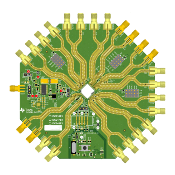
LMX1906-SP Evaluation Module
Description
The LMX1906-SP evaluation module (EVM) is
designed to evaluate the performance of the
LMX1906-SP, which is a four-output, ultra-low
additive jitter radio-frequency (RF) buffer, divider and
multiplier. The device can buffer RF frequencies up
to 18 GHz, multiply RF outputs up to 6.4 GHz,
and divide outputs by up to 6.4 GHz. This board
consists of an LMX1906-SP device and an integrated
USB2ANY programmer.
Features
•
300-MHz to 18-GHz output frequency
•
4 high-frequency clocks with corresponding
SYSREF outputs
– Shared divide by 2, 3, 4, 5, 6, 7 and 8
SNAU288 – DECEMBER 2023
Submit Document Feedback
– Shared programmable multiplier ×2, ×3, and ×4
•
3.3-V supply voltage (with onboard 2.5-V LDOs) or
2.5-V supply voltage (with LDOs bypassed)
•
–55ºC to +125ºC operating temperature (with
onboard MCU bypassed)
•
Optional pin mode control without register
programming
Applications
•
General purpose:
– Data converter clocking
– Clock distribution/multiplication/division
•
Aerospace and defense:
–
–
–
– Phased array antenna/beam forming
Copyright © 2023 Texas Instruments Incorporated
Radar
Electronic warfare
Seeker front end
LMX1906-SP Evaluation Module
Description
1
Advertisement

Related Manuals for Texas Instruments LMX1906-SP


Summary of Contents for Texas Instruments LMX1906-SP
- Page 1 The device can buffer RF frequencies up programming to 18 GHz, multiply RF outputs up to 6.4 GHz, Applications and divide outputs by up to 6.4 GHz. This board consists of an LMX1906-SP device and an integrated • General purpose: USB2ANY programmer. – Data converter clocking –...
-
Page 2: Kit Contents
2.5-V. The EVM contains LMX1906-SP, two LDOs, a microcontroller and an IO expander. LMX1906-SP and the LDOs can support –55ºC to +125ºC operation. For high temperature evaluation, use an USB2ANY dongle to control the EVM. -
Page 3: Connection Diagram
2-CH Arbitrary Function Generator Balun 1.3V ± 0.2V High-Quality Signal Generator PC with TICSPro & Signal Analyzer device profile installed Figure 2-1. EVM Connection Diagram SNAU288 – DECEMBER 2023 LMX1906-SP Evaluation Module Submit Document Feedback Copyright © 2023 Texas Instruments Incorporated... - Page 4 LOGICH) J37-J38 (Pulled LOW) When LOGICEN is set to low, all FPGA/LOGIC circuits and the SYSREF sub-system are deactivated and SPI cannot re-enable. LMX1906-SP Evaluation Module SNAU288 – DECEMBER 2023 Submit Document Feedback Copyright © 2023 Texas Instruments Incorporated...
- Page 5 This allows users to toggle pin modes through the GUI as well. If the user wishes to evaluate the LMX1906-SP without MCU control (physical pin strapping), then make sure no jumpers are present on any of the pin state headers.
- Page 6 2. Only divider values of 2/3/4 are available in pin mode. Divider values of 5 , 6 , 7 & 8 are valid divider values only when in SPI mode. LMX1906-SP Evaluation Module SNAU288 – DECEMBER 2023 Submit Document Feedback Copyright © 2023 Texas Instruments Incorporated...
-
Page 7: Output Connections
2.1.5.2 Header Information The LMX1906-SP EVM can be operated in either pin mode or SPI mode. Pin mode allows basic configuration of the LMX1906-SP device without the need of a microcontroller. SPI mode provides full customization of the LMX1906-SP device. - Page 8 2. Set SYSREF_MODE (R17[1:0]) = Generator Mode Continuous (0x1) Figure 2-2. How to Enable Continuous SYSREF and Set SYSREFREQ 3. Set SYSREFREQ_FORCE (R72[2:1]) = HIGH Figure 2-3. SYSREFREQ_FORCE LMX1906-SP Evaluation Module SNAU288 – DECEMBER 2023 Submit Document Feedback Copyright © 2023 Texas Instruments Incorporated...
- Page 9 Hardware 2.1.5.5 Multiplier Mode Example To set LMX1906-SP to multiplier mode by using SPI, follow the steps below: Set CLK_MUX (R25[2:0] = Multiplier (0x3). Figure 2-4. Selecting Multiplier Mode Set CLK_MULT (R25[5:3]) to appropriate multiplier value for respective CLKIN frequency.
- Page 10 Hardware www.ti.com Press Calibrate Multiplier button in GUI. Figure 2-6. Calibrate Multiplier 2.1.5.6 Divider Mode Example To set LMX1906-SP to divider mode via SPI do the following: Set CLK_MUX (R25[2:0] = Divider (0x2). Refer to image above in Section 2.1.5.5.
- Page 11 PIN MODES section. Figure 2-8. Config of TCA9535 Successful configuration of the IO expander results in a TCA9535 one-time configuration complete. Re-run if USB2ANY is disconnected. SNAU288 – DECEMBER 2023 LMX1906-SP Evaluation Module Submit Document Feedback Copyright © 2023 Texas Instruments Incorporated...
- Page 12 The user is now able to change the states of the pin mode headers via the IO expander by pulling pins either LOW or HIGH directly without the need of a physical short. CLKx_EN and Device mode options. Figure 2-10. Pin Mode Options LMX1906-SP Evaluation Module SNAU288 – DECEMBER 2023 Submit Document Feedback Copyright © 2023 Texas Instruments Incorporated...
- Page 13 Chooses RF output power for all CLKOUTx. Figure 2-11. pinPWRSEL Chooses the corresponding divider value when in divider mode or multiplier value in multiplier mode. Figure 2-12. pinDIVSEL SNAU288 – DECEMBER 2023 LMX1906-SP Evaluation Module Submit Document Feedback Copyright © 2023 Texas Instruments Incorporated...
-
Page 14: Software Description
(EVM) through the on-board USB2ANY interface. 3.3 USB2ANY Interface The on-board USB2ANY interface provides a bridge between TICS Pro software and the LMX1906-SP device. When the on-board USB2ANY controller is first connected to a PC, or if the firmware revision for the controller does not match with the version used by TICS Pro, a firmware update to the controller is required. - Page 15 9. Click the Identify button, the LED in the USB2ANY interface flashes. Figure 3-6. Identify USB2ANY Controller 10. Now, the USB2ANY is ready to use. Click the Close button to close the window. SNAU288 – DECEMBER 2023 LMX1906-SP Evaluation Module Submit Document Feedback Copyright © 2023 Texas Instruments Incorporated...
- Page 16 The blue trace is the reference clock from SMA100B and the yellow trace is the 800 MHz buffered output. Figure 4-2. 800-MHz Buffer Mode Signal Analyzer Plot LMX1906-SP Evaluation Module SNAU288 – DECEMBER 2023 Submit Document Feedback Copyright © 2023 Texas Instruments Incorporated...
- Page 17 The yellow trace is the 400 MHz divided output. Figure 4-3. 800-MHz Divide-by-2 Mode Signal Analyzer Plot The yellow trace is the 3200 MHz output. SNAU288 – DECEMBER 2023 LMX1906-SP Evaluation Module Submit Document Feedback Copyright © 2023 Texas Instruments Incorporated...
- Page 18 For continuous mode, a HIGH signal must be seen on SYSREFREQ pins continuously. For pulsed generator mode, a LOW→HIGH transition must be seen on SYSREFREQ pins to trigger the pulser. For repeater mode, the output follows the input state. LMX1906-SP Evaluation Module SNAU288 – DECEMBER 2023 Submit Document Feedback Copyright © 2023 Texas Instruments Incorporated...
- Page 19 Implementation Results Figure 4-5. 800-MHz Buffer Mode With 10 MHz SYSREF SNAU288 – DECEMBER 2023 LMX1906-SP Evaluation Module Submit Document Feedback Copyright © 2023 Texas Instruments Incorporated...
- Page 20 GUI calculates the correct step values to achieve the requested delay as closely as possible. Alternately, the register-based delay fields can be stepped through or programmed to achieve the same result. Figure 4-6. SYSREF Delay in 5-Code Steps LMX1906-SP Evaluation Module SNAU288 – DECEMBER 2023 Submit Document Feedback Copyright © 2023 Texas Instruments Incorporated...
- Page 21 Hardware Design Files 5 Hardware Design Files 5.1 Schematic Figure 5-1. Power Supply SNAU288 – DECEMBER 2023 LMX1906-SP Evaluation Module Submit Document Feedback Copyright © 2023 Texas Instruments Incorporated...
- Page 22 Hardware Design Files www.ti.com Figure 5-2. Power Supply LMX1906-SP Evaluation Module SNAU288 – DECEMBER 2023 Submit Document Feedback Copyright © 2023 Texas Instruments Incorporated...
- Page 23 Hardware Design Files Figure 5-3. LMX1906-SP SNAU288 – DECEMBER 2023 LMX1906-SP Evaluation Module Submit Document Feedback Copyright © 2023 Texas Instruments Incorporated...
- Page 24 Hardware Design Files www.ti.com Figure 5-4. Clock Input, Clock Output Interface LMX1906-SP Evaluation Module SNAU288 – DECEMBER 2023 Submit Document Feedback Copyright © 2023 Texas Instruments Incorporated...
- Page 25 Hardware Design Files Figure 5-5. IO Interface SNAU288 – DECEMBER 2023 LMX1906-SP Evaluation Module Submit Document Feedback Copyright © 2023 Texas Instruments Incorporated...
- Page 26 Hardware Design Files www.ti.com Figure 5-6. USB2ANY Interface LMX1906-SP Evaluation Module SNAU288 – DECEMBER 2023 Submit Document Feedback Copyright © 2023 Texas Instruments Incorporated...
-
Page 27: Pcb Layout
Hardware Design Files 5.2 PCB Layout Figure 5-7. Top Layer Figure 5-8. Layer 2 (RF GND) SNAU288 – DECEMBER 2023 LMX1906-SP Evaluation Module Submit Document Feedback Copyright © 2023 Texas Instruments Incorporated... - Page 28 Hardware Design Files www.ti.com Figure 5-9. Layer 3 (Power) Figure 5-10. Layer 4 (Power) LMX1906-SP Evaluation Module SNAU288 – DECEMBER 2023 Submit Document Feedback Copyright © 2023 Texas Instruments Incorporated...
- Page 29 Hardware Design Files Figure 5-11. Layer 5 (GND) Figure 5-12. Bottom Layer SNAU288 – DECEMBER 2023 LMX1906-SP Evaluation Module Submit Document Feedback Copyright © 2023 Texas Instruments Incorporated...
- Page 30 FR4 (Er = 4.27) Signal GND layer 2 FR4 (Er = 3.88) GND layer FR4 (Er = 4.21) o m layer ¡ Figure 5-13. PCB Layer Stack-Up LMX1906-SP Evaluation Module SNAU288 – DECEMBER 2023 Submit Document Feedback Copyright © 2023 Texas Instruments Incorporated...
- Page 31 J14, J28, J29, J40 Header, 100mil, 3x1, Gold, TSW-103-07-G-S Samtec J15, J17, J19, J21, J23, CONN SMA JACK STR CON-SMA-EDGE-S EDGE MNT RF Solutions Ltd. J25, J30 SNAU288 – DECEMBER 2023 LMX1906-SP Evaluation Module Submit Document Feedback Copyright © 2023 Texas Instruments Incorporated...
- Page 32 SH-J1, SH-J2, SH-J3, SH- Shunt, 2.54 mm, Gold, Black 60900213421 2.54 mm Wurth Elektronik TP1, TP4, TP5, TP6, TP9, Test Point, Miniature, White 5002 Keystone TP10, TP11 LMX1906-SP Evaluation Module SNAU288 – DECEMBER 2023 Submit Document Feedback Copyright © 2023 Texas Instruments Incorporated...
- Page 33 Single Schmitt-Trigger Buffer SN74LVC1G17DBVR DBV0005A Texas Instruments Low-Power I/O Expander TCA9535RTWR RTW0024B Texas Instruments Crystal, 24.000 MHz, 20 pF ECS-240-20-5PX-TR 11.4×4.3×3.8 mm ECS Inc. SNAU288 – DECEMBER 2023 LMX1906-SP Evaluation Module Submit Document Feedback Copyright © 2023 Texas Instruments Incorporated...
- Page 34 Register readback requires programming MUXOUT_EN = 1 and MUXOUT_SEL = 1. The GUI also prompts to configure this register before attempting any readback operation. • The POR current of the LMX1906-SP EVM is approximately 17 mA with the LDOs bypassed & 975 mA with LDOs enabled. –...
- Page 35 1.5-V supply through the internal 100-Ω impedance. An arbitrary function generator is recommended if possible. 6.2 Trademarks All trademarks are the property of their respective owners. SNAU288 – DECEMBER 2023 LMX1906-SP Evaluation Module Submit Document Feedback Copyright © 2023 Texas Instruments Incorporated...
- Page 36 STANDARD TERMS FOR EVALUATION MODULES Delivery: TI delivers TI evaluation boards, kits, or modules, including any accompanying demonstration software, components, and/or documentation which may be provided together or separately (collectively, an “EVM” or “EVMs”) to the User (“User”) in accordance with the terms set forth herein.
- Page 37 www.ti.com Regulatory Notices: 3.1 United States 3.1.1 Notice applicable to EVMs not FCC-Approved: FCC NOTICE: This kit is designed to allow product developers to evaluate electronic components, circuitry, or software associated with the kit to determine whether to incorporate such items in a finished product and software developers to write software applications for use with the end product.
- Page 38 www.ti.com Concernant les EVMs avec antennes détachables Conformément à la réglementation d'Industrie Canada, le présent émetteur radio peut fonctionner avec une antenne d'un type et d'un gain maximal (ou inférieur) approuvé pour l'émetteur par Industrie Canada. Dans le but de réduire les risques de brouillage radioélectrique à...
- Page 39 www.ti.com EVM Use Restrictions and Warnings: 4.1 EVMS ARE NOT FOR USE IN FUNCTIONAL SAFETY AND/OR SAFETY CRITICAL EVALUATIONS, INCLUDING BUT NOT LIMITED TO EVALUATIONS OF LIFE SUPPORT APPLICATIONS. 4.2 User must read and apply the user guide and other available documentation provided by TI regarding the EVM prior to handling or using the EVM, including without limitation any warning or restriction notices.
- Page 40 Notwithstanding the foregoing, any judgment may be enforced in any United States or foreign court, and TI may seek injunctive relief in any United States or foreign court. Mailing Address: Texas Instruments, Post Office Box 655303, Dallas, Texas 75265 Copyright © 2023, Texas Instruments Incorporated...
- Page 41 TI products. TI’s provision of these resources does not expand or otherwise alter TI’s applicable warranties or warranty disclaimers for TI products. TI objects to and rejects any additional or different terms you may have proposed. IMPORTANT NOTICE Mailing Address: Texas Instruments, Post Office Box 655303, Dallas, Texas 75265 Copyright © 2023, Texas Instruments Incorporated...