Advertisement
Quick Links
Model
A/V DOLBY DIGITAL RECEIVER
Cinema Propack
ESD WARNING....................................2
LEAKAGE TESTING...............................3
BASIC SPECIFICATIONS.......................4
FRONT PANEL CONTROLS.....................5
INFORMATION DISPLAY........................7
REAR PANEL CONNECTIONS................8
REMOTE CONTROL FUNCTIONS..........10
INSTALLATION DIAGRAMS...................14
OPERATION.......................................17
TROUBLESHOOTING GUIDE................20
DCR600II
Service Manual
- CONTENTS -
JBL Consumer Products
250 Crossways Park Dr.
Woodbury, New York 11797
™
600II System
PROCESSOR RESET...........................20
TECH TIP JBLTT2003-01.......................23
UNIT EXPLODED VIEW.........................24
EXPLODED VIEW PARTS LIST..............25
BLOCK DIAGRAM...............................26
PCB DRAWINGS.................................27
ELECTRICAL PARTS LIST....................37
PACKAGING PARTS LIST......................68
SEMICONDUCTOR PINOUTS...............69
SCHEMATICS....................................115
Rev2
7/2005
Advertisement

Related Manuals for JBL DCR600II


Summary of Contents for JBL DCR600II
-
Page 1: Table Of Contents
EXPLODED VIEW PARTS LIST…………..25 INFORMATION DISPLAY………..…..……..7 BLOCK DIAGRAM……………….…………26 REAR PANEL CONNECTIONS………….…8 PCB DRAWINGS……………….……..……27 REMOTE CONTROL FUNCTIONS……….10 ELECTRICAL PARTS LIST…….………….37 INSTALLATION DIAGRAMS……………..14 PACKAGING PARTS LIST………..………68 SEMICONDUCTOR PINOUTS……………69 OPERATION…………………..….…………17 SCHEMATICS…………………..…..……..115 TROUBLESHOOTING GUIDE…..……..…20 JBL Consumer Products 250 Crossways Park Dr. Woodbury, New York 11797 Rev2 7/2005... - Page 2 DCR600II Some semiconductor (solid state) devices can be damaged easily by static electricity. Such components commonly are called Electrostatically Sensitive (ES) Devices. Examples of typical ES devices are integrated circuits and some field effect transistors and semiconductor "chip" components. The following techniques should be used to help reduce the incidence of component damage caused by static electricity.
- Page 3 DCR600II Before returning the unit to the user, perform the following safety checks : 1. Inspect all lead dress to make certain that leads are not pinched or that hardware is not lodged between the chassis and other metal parts in the unit.
- Page 4 500mV at 1kHz, ±75kHz Deviation JBL On Screen Library is a trademark of JBL, Inc. (patent pending). JBL One-Click is a trademark of JBL, Inc. (patent pending). *Manufactured under license from Dolby Laboratories. “Dolby,” “Pro Logic,” “AC-3” and the Double-D symbol are trademarks of Dolby Laboratories.
-
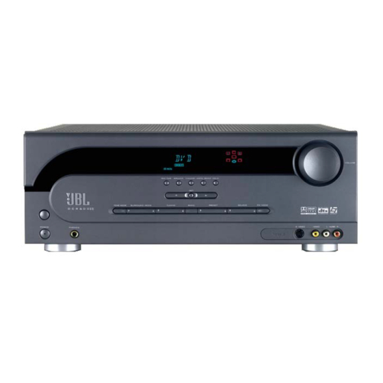
Page 5: Front Panel Controls
DCR600II DCR600 Front Panel Controls 1 Main Power Switch: Press this button to of headphones. Be certain that the headphones are not always available. (See page 52 for have a standard 1/4" stereo phone plug. Note more information about surround modes.) apply power to the DCR600 . -
Page 6: Information Display
DCR600II 9 Tuner Band Selector: Pressing this button $ Video 3 Audio Input Jacks: These Once the desired brightness level is selected, it will remain in effect until it is changed again will automatically switch the DCR600 to the audio/video jacks may be used for temporary or until the unit is turned off. - Page 7 DCR600II DCR600 Front Panel Information Display 96KHz 192KHz A Bitstream Indicators: When the input is I Logic 7 Mode: Indicates that the Logic 7 N Preset Number/Sleep Timer: In Tuner a digital source, these indicators display the mode is in use. Logic 7C 5.1-CINEMA mode, these numbers indicate the preset mem- specific type of data signal.
-
Page 8: Rear Panel Connections
DCR600II DCR600 Rear Panel Connections MODEL NO. DCR600 IMPORTANT NOTES ¡ Coaxial Digital Audio Output: Connect § Tape Inputs: Connect to PLAY/OUT jacks to the coaxial digital input connector on a of an audio recorder. A. The AC plug connections should always be CD-R or MiniDisc recorder. - Page 9 DCR600II ¤ Video 1 Video Inputs: Connect to NOTE: When making speaker connections always make certain to maintain correct PLAY/OUT composite or S-Video jacks on a polarity by connecting the colored (+) terminals VCR or other video source. on the DCR600 to the red (+) terminals on the ‹...
-
Page 10: Remote Control Functions
DVD changer. Press the Main Button h to return the remote to control of the DCR600 receiver. IMPORTANT NOTE: The remote control for the JBL Cinema ProPack 600 may be pro- grammed to control up to eight devices, includ- ing the DCR600 and DVD600 . - Page 11 3) It will switch to the page for the tape deck may find it convenient to connect your televi- u All Off: This feature of the JBL One-Click™ whose codes have been programmed into the sion to this input, particularly since it does not...
- Page 12 DCR600II DVD600 is selected, this button is used to When a DVD encoded with multiple-angle to select the channel being adjusted, change the subtitle choice. For other video information is playing, press to change the followed by the Set Button .
- Page 13 DCR600II Preset Up/Down/Slow-Play NOTE: When any of the following buttons Play/Pause Button is pressed – Buttons: When the tuner is in use, press these is pressed while the remote has again, even if the unit has been turned off in...
-
Page 14: Installation Diagrams
DCR600II Quick Installation Diagrams BASIC INSTALLATION: Your TV must at a minimum have a composite video input (this connector usually has a yellow-colored core), and Left (usually has a white-colored core) and Right (red-colored core) Stereo audio preamp-level RCA outputs. All wires for this hookup are included. - Page 15 DCR600II Quick Installation Diagrams ALTERNATE INSTALLATION FOR BETTER PICTURE QUALITY: Your TV must have an S-Video input, and Left (usually has a white-colored core) and Right (red-colored core) Stereo audio preamp-level RCA outputs. Two pieces of S-Video cable are not included and should be purchased separately.
- Page 16 DCR600II Quick Installation Diagrams ALTERNATE INSTALLATION FOR BEST PICTURE QUALITY: Your TV must have Y/Pr/Pb component video inputs (three separate RCA connectors with red-, blue- and green-colored cores), and Left (usually has a white-colored core) and Right (red-colored core) Stereo audio preamp-level RCA outputs. The component video cable is not included and should be purchased separately.
- Page 17 DCR600II Operating the DCR600 Receiver DCR600 will automatically select and switch to ferent methods of encoding the signals, and Selecting a Surround Mode the correct mode (Dolby Digital or DTS), regardless thus they require different decoding circuits to One of the most important features of the of the mode that has been previously selected.
- Page 18 DCR600II Operating the DCR600 Receiver When the digital source is playing, the DCR600 present, all modes except Dolby Digital and DTS and not through any fault of the DCR600 . This will automatically detect whether it is a multi- are available.
- Page 19 DCR600II Operating the DCR600 Receiver Preset Tuning 5. When a Dolby Digital or DTS source is playing, Station Selection 1. Press the AM/FM Tuner Select Button k Using the remote, up to 30 stations may be it is not possible to make an analog recording using the Tape ¶...
-
Page 20: Processor Reset
• Amplifier is in Protection mode • Contact your local JBL service center. due to internal problems No sound from any speaker • No audio signal is being transmitted •... - Page 21 DCR600II Troubleshooting No sound from one speaker • No audio signal is being transmitted • Check all wires and connections between the DCR600 to the speakers speakers. Make sure all wires are connected. Make sure none of the speaker wires are frayed, cut or punctured.
- Page 22 DCR600II Troubleshooting Disc does not play • Disc loaded improperly • Load disc label-side up. • Incorrect disc type • Check to see that disc is CD, CD-R, CD-RW, DVD-Movie, MP3 or Video CD; other types will not play. • Invalid Region Code •...
- Page 23 JSR400 DCR600 DCR600II Subject: Backup Memory on JBL Receivers In the event of the complaint: “the receiver is losing its memory (any programmed system settings) when the unit is turned off, or after the unit is unplugged (briefly*)”: Check and replace:...
- Page 24 DCR600II...
- Page 25 DCR600II...
- Page 26 DCR600II DCR600IIBLOCK .sch-1 - Wed Sep 11 10:49:20 2002...
- Page 27 DCR600II...
- Page 28 DCR600II...
- Page 29 DCR600II...
- Page 30 DCR600II...
- Page 31 DCR600II...
- Page 32 DCR600II...
- Page 33 DCR600II...
- Page 34 DCR600II...
- Page 35 DCR600II...
- Page 36 DCR600II...
- Page 37 DCR600II DCR600II Electrical Parts List Ref. Designator Part Number Description AMP PCB Capacitors C601 20178680 CE 4U7F +20% 50.0V 85C 20202890 C602 20936650 CC 100P0F +10% -10% 50.0V Y5P C603 55126070 CC 680P0F +10% -10% 50.0V 2B4 C604 20251930 CE 22U0F +20% 16.0V 85C...
- Page 38 DCR600II Ref. Designator Part Number Description AMP PCB C663 11054760 CE 100U0F +20% 63.0V 85C C664 13055500 CE 10U0F +20% 50.0V 85C C665 13055500 CE 10U0F +20% 50.0V 85C C668 20267420 CE 1U0F +20% 50.0V 105C C669 20178680 CE 4U7F +20% 50.0V 85C 20202890...
- Page 39 DCR600II Ref. Designator Part Number Description AMP PCB Q637 20556600 TR-SHPLF KTC3200BL N 100MI0A 120V Q639 55133260 TR-SLPLF KTA1024 Y P 50MI0A -150V Q640 55133240 TR-SLPLF KTC3206 Y N 50MI0A 150V Q645 20556600 TR-SHPLF KTC3200BL N 100MI0A 120V Q646 55133230...
- Page 40 DCR600II Ref. Designator Part Number Description AMP PCB Resistors R601 11059640 RCF 1K0 OHM +5% 250MI0W R602 30939490 RCF 33K0 OHM +5% 250MI0W R603 30939370 RCF 15R0 OHM +5% 250MI0W R604 30939370 RCF 15R0 OHM +5% 250MI0W R605 11059630 RCF 680R0 OHM +5% 250MI0W...
- Page 41 DCR600II Ref. Designator Part Number Description AMP PCB R672 50882950 RCF 100R0 OHM +5% 250MI0W R673 50882950 RCF 100R0 OHM +5% 250MI0W R677 80437010 RCF 1K8 OHM +5% 250MI0W R678 20469460 RCF 2K2 OHM +5% 250MI0W R679 80436990 RCF 910R0 OHM +5% 250MI0W...
- Page 42 DCR600II Ref. Designator Part Number Description AMP PCB R754 70434970 RCF 3R3 OHM +5% 250MI0W R755 70434970 RCF 3R3 OHM +5% 250MI0W R756 50882950 RCF 100R0 OHM +5% 250MI0W R757 50882950 RCF 100R0 OHM +5% 250MI0W R761 80437010 RCF 1K8 OHM +5% 250MI0W...
- Page 43 DCR600II Ref. Designator Part Number Description AMP PCB R828 80437000 RCF 1K2 OHM +5% 250MI0W R829 50882980 RCF 820R0 OHM +5% 250MI0W R830 80436990 RCF 910R0 OHM +5% 250MI0W R831 11059590 RCF 82R0 OHM +5% 250MI0W R832 11059590 RCF 82R0 OHM +5% 250MI0W...
- Page 44 DCR600II Ref. Designator Part Number Description DSP PCB C214 11059320 CCCFMIN 1N0F +10% -10% 50.0V X7R C215 11059320 CCCFMIN 1N0F +10% -10% 50.0V X7R 11059340 CCCFMIN 10N0F +10% -10% 50.0V X7R 20267320 CCCFMIN 220N0F +80% -20% 50.0V Y5V 11059340 CCCFMIN 10N0F +10% -10% 50.0V X7R 40435540 CCCFMIN 5N6F +10% -10% 50.0V X7R...
- Page 45 DCR600II Ref. Designator Part Number Description DSP PCB 20267290 CCCFMIN 100N0F +80% -20% 50.0V Y5V 20267290 CCCFMIN 100N0F +80% -20% 50.0V Y5V 20267290 CCCFMIN 100N0F +80% -20% 50.0V Y5V 40435180 CCCFMIN 47P0F +5% -5% 50.0V NP0 30938730 CCCFMIN 220P0F +5% -5% 50.0V NP0 20468970 CCCFMIN 330P0F +5% -5% 50.0V NP0...
- Page 46 DCR600II Ref. Designator Part Number Description DSP PCB IC10 55133310 IC-LOGIC M74HCU04M1R INVERTER HCT IC11 20920060 IC-OPERAMP KIA4558F DUAL OP IC12 20920060 IC-OPERAMP KIA4558F DUAL OP IC14 55125410 IC-LOWFREQ CS8415A-CS DSP IC18 55125420 IC-LOGIC 74VHC244MX INVERTER CMOS IC19 55125420 IC-LOGIC 74VHC244MX INVERTER CMOS...
- Page 47 DCR600II Ref. Designator Part Number Description DSP PCB R157 20471950 RMGCFMIN 1K0 OHM +5% 100MI0W R158 20471990 RMGCFMIN 12K0 OHM +5% 100MI0W R159 20471990 RMGCFMIN 12K0 OHM +5% 100MI0W 11066440 RMGCFMIN 3K3 OHM +5% 100MI0W 30944310 RMGCFMIN 4K7 OHM +5% 100MI0W...
- Page 48 DCR600II Ref. Designator Part Number Description DSP PCB 70434250 RMGCFMIN 15K0 OHM +5% 100MI0W 50886610 RMGCFMIN 10K0 OHM +5% 100MI0W 30944250 RMGCFMIN 10R0 OHM +5% 100MI0W 80440390 RMGCFMIN 2K2 OHM +5% 100MI0W 80440510 RMGCFMIN 0 OHM +0% 100MI0W 90574400 RMGCFMIN 470R0 OHM +5% 100MI0W...
- Page 49 DCR600II Ref. Designator Part Number Description DSP PCB 50886610 RMGCFMIN 10K0 OHM +5% 100MI0W 80440420 RMGCFMIN 33K0 OHM +5% 100MI0W R188 30944330 RMGCFMIN 20K0 OHM +5% 100MI0W 30944310 RMGCFMIN 4K7 OHM +5% 100MI0W R190 50886610 RMGCFMIN 10K0 OHM +5% 100MI0W...
- Page 50 DCR600II Ref. Designator Part Number Description DSP PCB BD26 80440510 RMGCFMIN 0 OHM +0% 100MI0W BD27 80440510 RMGCFMIN 0 OHM +0% 100MI0W BD29 80440510 RMGCFMIN 0 OHM +0% 100MI0W BD30 30944260 RMGCFMIN 22R0 OHM +5% 100MI0W BD31 30944260 RMGCFMIN 22R0 OHM +5% 100MI0W...
- Page 51 DCR600II Ref. Designator Part Number Description FRONT PCB C209 20267290 CCCFMIN 100N0F +80% -20% 50.0V Y5V C211 15070900 CCCFMIN 820P0F +10% -10% 50.0V NP0 C212 15070900 CCCFMIN 820P0F +10% -10% 50.0V NP0 C213 20267290 CCCFMIN 100N0F +80% -20% 50.0V Y5V...
- Page 52 DCR600II Ref. Designator Part Number Description FRONT PCB R201 50886610 RMGCFMIN 10K0 OHM +5% 100MI0W R202 50886610 RMGCFMIN 10K0 OHM +5% 100MI0W R203 50886610 RMGCFMIN 10K0 OHM +5% 100MI0W R204 20471950 RMGCFMIN 1K0 OHM +5% 100MI0W R205 20471950 RMGCFMIN 1K0 OHM +5% 100MI0W...
- Page 53 DCR600II Ref. Designator Part Number Description FRONT PCB FINGER 55178960 AC SPRING PLATE SPRING GND C5212 0.2T AVR520 FL201 55182450 DISPLAY VFD HNA-16LL18 JA201 55113740 CON PHONO SCKT RCA-307 3 PINS JA202 55113960 CON DIN SCKT SOCKET CONNECTOR SVHS EST-S408J...
- Page 54 DCR600II Ref. Designator Part Number Description KEY PCB R419 11066460 RMGCFMIN 8K2 OHM +5% 100MI0W R420 90574430 RMGCFMIN 18K0 OHM +5% 100MI0W R421 50886540 RMGCFMIN 330R0 OHM +5% 100MI0W R421 60444370 RMGCFMIN 180R0 OHM +5% 100MI0W R422 20471950 RMGCFMIN 1K0 OHM +5% 100MI0W...
- Page 55 DCR600II Ref. Designator Part Number Description KEY PCB BD305 55126650 FBEAD SURFACE MT 300OHM FCM2012V-301T07 BD306 55126530 FBEAD SURFACE MT 300OHM CHIP FERRITE BEAD U BD306 55126650 FBEAD SURFACE MT 300OHM FCM2012V-301T07 SW401-420 55145270 SWITACT VERTICAL TACTILE F/B 50MI0A 12.0V 500MI0OHM 1T 1P...
- Page 56 DCR600II Ref. Designator Part Number Description MAIN PCB C454 50882360 CCCFMIN 33P0F +5% -5% 50.0V NP0 C455 30938730 CCCFMIN 220P0F +5% -5% 50.0V NP0 C460 11058670 CCCFMIN 100P0F +5% -5% 50.0V NP0 C952 20267290 CCCFMIN 100N0F +80% -20% 50.0V Y5V...
- Page 57 DCR600II Ref. Designator Part Number Description MAIN PCB C402 20266840 CPF 8N2F +10% 50.0V C403 20268860 CE 3U3F +20% 50.0V 85C C404 20268860 CE 3U3F +20% 50.0V 85C C405 20266120 CPF 1N0F +10% 50.0V C406 20266120 CPF 1N0F +10% 50.0V...
- Page 58 DCR600II Ref. Designator Part Number Description MAIN PCB C954 20268880 CE 10U0F +20% 50.0V 85C C955 20268880 CE 10U0F +20% 50.0V 85C C956 20268880 CE 10U0F +20% 50.0V 85C C958 20268880 CE 10U0F +20% 50.0V 85C C959 20268880 CE 10U0F +20% 50.0V 85C...
- Page 59 DCR600II Ref. Designator Part Number Description MAIN PCB D418 20526960 D-ZENER 1N5231B 5.1V 500MI0W Q102 20508210 TR-SLPLF KTA1266 Y P 150MI0A Q103 20508210 TR-SLPLF KTA1266 Y P 150MI0A Q104 55133250 TR-SLPLF 2SC1740S R N 150MI0A 50V Q105 55133250 TR-SLPLF 2SC1740S R N 150MI0A 50V...
- Page 60 DCR600II Ref. Designator Part Number Description MAIN PCB R137 20471950 RMGCFMIN 1K0 OHM +5% 100MI0W R138 80440390 RMGCFMIN 2K2 OHM +5% 100MI0W R139 30944310 RMGCFMIN 4K7 OHM +5% 100MI0W R140 30944310 RMGCFMIN 4K7 OHM +5% 100MI0W R150 50886630 RMGCFMIN 100K0 OHM +5% 100MI0W...
- Page 61 DCR600II Ref. Designator Part Number Description MAIN PCB R328 80440390 RMGCFMIN 2K2 OHM +5% 100MI0W R330 70434230 RMGCFMIN 1K2 OHM +5% 100MI0W R331 80440390 RMGCFMIN 2K2 OHM +5% 100MI0W R333 11066440 RMGCFMIN 3K3 OHM +5% 100MI0W R334 11066440 RMGCFMIN 3K3 OHM +5% 100MI0W...
- Page 62 DCR600II Ref. Designator Part Number Description MAIN PCB R463 50886630 RMGCFMIN 100K0 OHM +5% 100MI0W R464 90574410 RMGCFMIN 910R0 OHM +5% 100MI0W R465 30944340 RMGCFMIN 27K0 OHM +5% 100MI0W R465 60444400 RMGCFMIN 22K0 OHM +5% 100MI0W R465 90574430 RMGCFMIN 18K0 OHM +5% 100MI0W...
- Page 63 DCR600II Ref. Designator Part Number Description MAIN PCB R114 11059600 RCF 120R0 OHM +5% 250MI0W R115 20469460 RCF 2K2 OHM +5% 250MI0W R130 20469460 RCF 2K2 OHM +5% 250MI0W R148 11059600 RCF 120R0 OHM +5% 250MI0W R158 50882950 RCF 100R0 OHM +5% 250MI0W...
- Page 64 DCR600II Ref. Designator Part Number Description MAIN PCB R128 20696190 RW 100MI0 OHM +5% 5.0W 260PPM/'C 260PPM/'C R141-144 55154180 RMFF 270MI0 OHM +10% 1.0W R400 90572170 RMOF 270R0 OHM +5% 1.0W R401 90572160 RMOF 220R0 OHM +5% 1.0W R401 90572170 RMOF 270R0 OHM +5% 1.0W...
- Page 65 DCR600II Ref. Designator Part Number Description MAIN PCB JK118 55208270 CONN-SPE TERMINAL SPKR 8P SH FE 19MM 8 BN 0 0 L900-905 21070690 LFA 1MM 10MM 7 LEFT 0.0MM NONE RY900 55091520 RELAYPWR 24.0V 1K1OHM 5.0A RY900 55127410 RELAYPWR 24.0V 1K1OHM 5.0A 30.0V...
- Page 66 DCR600II Ref. Designator Part Number Description POWER PCB R100 55180100 RA 3M3 OHM +10% 500MI0W Miscellaneous CP102 55123510 CON 3.96MM PITCH HEADER 2 POS MOLEX 35328-0210 CP303 55090060 CONN 2.0MM 7 MA ST NAT LW2002P07 0 0 CP400 55142040 WIRECONASY UNIQUE 10P 320MM UL1007 PVC DISCRETE 20 1...
- Page 67 DCR600II Ref. Designator Part Number Description SUBWOOFER PCB Semiconductors 20496510 D-SLP 1SS355 35.0V 225MI0A 20496510 D-SLP 1SS355 35.0V 225MI0A 20920060 IC-OPERAMP KIA4558F DUAL OP 20920060 IC-OPERAMP KIA4558F DUAL OP 70436540 D-SLP 1N4148 100.0V 150E-3A 70436540 D-SLP 1N4148 100.0V 150E-3A Q410...
- Page 68 15 foot cable set, receiver to subwoofer sal063-52 5 foot triple, red/wht/yellow RCA cable, DCR600II receiver to TV set 55176530 3 foot single orange RCA cable, DCR600II receiver to DVD600II 55186190 3 foot single yellow RCA cable, DCR600II receiver to DVD600II...
- Page 69 DCR600II...
- Page 70 DCR600II...
- Page 71 DCR600II...
- Page 72 DCR600II...
- Page 73 DCR600II...
- Page 74 DCR600II AT27LV010A Features • Fast Read Access Time - 90 ns • Dual Voltage Range Operation Low Voltage Power Supply Range, 3.0V to 3.6V or Standard 5V ± 10% Supply Range • Compatible with JEDEC Standard AT27C010 • Low Power CMOS Operation 20 µA max.
- Page 75 DCR600II Description (Continued) System Considerations The AT27LV010A is available in industry standard Switching between active and standby conditions via the JEDEC-approved one-time programmable (OTP) plastic Chip Enable pin may produce transient voltage excur- PLCC and TSOP packages. All devices feature two-line sions.
-
Page 76: Block Diagram
DCR600II AT27LV010A Absolute Maximum Ratings* Block Diagram Temperature Under Bias ....-40°C to +85°C Storage Temperature...... -65°C to +125°C Voltage on Any Pin with Respect to Ground......-2.0V to +7.0V Voltage on A9 with Respect to Ground ...... -2.0V to +14.0V Supply Voltage with Respect to Ground....... - Page 78 DCR600II...
- Page 79 DCR600II...
- Page 80 DCR600II...
- Page 81 DCR600II...
- Page 82 DCR600II...
- Page 83 Multimedia ICs Video signal switcher for AV amplifiers BA7626 / BA7626F The BA7626 and BA7626F are video signal switches that contain two five-channel analog multiplexers for switching chroma and audio signals, and two wide-band 6dB amplifiers. By simply adding transistor buffers to the outputs, it is possible to construct a record / playback switch for two record / playback VCRs, and three video playback machines (eg.
- Page 84 Multimedia ICs BA7626 / BA7626F • Block diagram Monitor OUT CTL A logic CTL E CTL B logic OUT2 CTL D CTL C • Truth table Monitor OUT OUT1 OUT2 ∗ ∗ ∗ — ∗ ∗ ∗ — ∗ ∗ ∗...
- Page 85 Multimedia ICs BA7626 / BA7626F • Equivalent input / output circuits (unless otherwise noted, Ta=25°C and V = 5V) Pin No. Pin name Standard voltage (no input signal) Equivalent input / output circuit 3.6V 4.3V 100µA CTL E CTL D CTL C 0.6V CTL B...
- Page 86 Triple 2-channel analog multiplexer / demultiplexer BU4053BC / BU4053BCF / BU4053BCFV The BU4053BC, BU4053BCF, and BU4053BCFV are multiplexers / demultiplexers capable of selecting and combin- ing analog signals and digital signals in a 2 ch × 3 configuration. Inhibit signals and control signals are used to turn on the switch corresponding to each of the channels.
- Page 87 8-bit compatible shift / store register BU4094BC / BU4094BCF / BU4094BCFV The BU4094BC, BU4094BCF, and BU4094BCFV are shift / store registers, each consisting of an 8-bit register and an 8-bit latch. As the data in the shift register can be latched by an asynchronous strobe input, it is possible to hold the output in the data transfer mode.
- Page 88 DCR600II www.fairchildsemi.com KA4558 Dual Operational Amplifier Features Descriptions • No frequency compensation required. The KA4558 is a monolithic integrated circuit designed for • No latch up. dual operational amplifier. • Large common mode and differential voltage range. • Parameter tracking over temperature range.
- Page 89 DCR600II...
- Page 90 DCR600II...
- Page 91 DCR600II...
- Page 92 DCR600II...
- Page 93 DCR600II...
- Page 94 DCR600II...
- Page 95 DCR600II...
- Page 96 DCR600II...
- Page 97 DCR600II...
- Page 98 DCR600II...
- Page 99 DCR600II...
- Page 100 DCR600II...
- Page 101 DCR600II...
- Page 102 DCR600II...
- Page 103 DCR600II...
- Page 104 DCR600II Ordering number : EN4817A CMOS LSI LC78211, 78212, 78213 Analog Function Switch Applications Package Dimensions Function switching under serial data control in amplifiers, unit: mm receivers, and other electronic equipment 3061-DIP30S Features [LC78211, 78212, 78213] • Two sets of eight (or in the LC78213, seven) built-in...
- Page 105 DCR600II LC78211, 78212, 78213 Pin Assignments Top view | ≥ | V Allowable Operating Ranges at Ta = 25°C, V = 0 V, Parameter Symbol Conditions Unit ≥ 12 V: V – V 18.5 Maximum supply voltage ≥ 12 V: V –...
- Page 106 DCR600II LC78211, 78212, 78213 Electrical Characteristics at Ta = 25°C, V = 0 V Parameter Symbol Conditions Unit I = 1 mA, V – V = 12 V: Ω L1 to L8, R1 to R8, LCOM1 to LCOM4, RCOM1 to RCOM4...
- Page 107 DCR600II LC78211, 78212, 78213 Continued from preceding page. No. 4817-4/6...
- Page 108 DCR600II LC78211, 78212, 78213 Pin Functions Internal equivalent circuit Pin function Power supply L1 to L8, R1 to R8, LCOM1 to LCOM4, See the block diagram. Analog switch input and output RCOM1 to RCOM4 Serial data input (Schmitt buffer) CL....Clock input CL, DI, CE DI....Data input...
- Page 109 DCR600II LC78211, 78212, 78213 2. DI, CL and CE Timing Data is read in on the rising edge of CL and latched on the falling edge of CE. 3. Notes on the Reset Pin The states of the analog switches are undefined when power is first applied. However, it is possible to use the reset pin to force all switches to the off state by connecting an RC circuit to this pin.
- Page 110 November 1995 MM54HC151 MM74HC151 8-Channel Digital Multiplexer General Description This high speed Digital multiplexer utilizes advanced silicon- All inputs are protected from damage due to static dis- gate CMOS technology Along with the high noise immunity charge by internal diode clamps to V and ground and low power dissipation of standard CMOS integrated cir- Features...
- Page 111 DCR600II...
- Page 112 DCR600II...
- Page 113 DCR600II...
- Page 114 DCR600II...
- Page 115 DCR600II...
- Page 116 DCR600II...
- Page 117 DCR600II...
- Page 118 DCR600II...
- Page 119 DCR600II...
- Page 120 DCR600II...
- Page 121 DCR600II...
- Page 122 DCR600II...
- Page 123 DCR600II...
- Page 124 DCR600II...
- Page 125 DCR600II...
- Page 126 DCR600II...
- Page 127 DCR600II...