Table of Contents
Advertisement
Quick Links
SAFETY PRECAUTION FOR SERVICE MANUAL ........................................................................................................... 2
SPECIFICATIONS ............................................................................................................................................................. 3
NAMES OF PARTS ........................................................................................................................................................... 4
DISASSEMBLY .................................................................................................................................................................. 7
REMOVING AND REINSTALLING THE MAIN PARTS ..................................................................................................... 9
WIRING PROCESS DIARGRAM ....................................................................................................................................... 9
ADJUSTMENT ................................................................................................................................................................. 10
DVD UNIT DOWNLOLD PROCEDURES ........................................................................................................................ 21
DESCRIPTION OF AND HOW TO AVOID ERROR AND ABNORMALITY INDICATIONS ............................................ 23
DESCRIPTION OF CIRCUIT FOR 1-BIT UNIT ............................................................................................................... 24
TO CHECK AND CANCEL PROTECT CIRCUIT DETECTION LINE .............................................................................. 25
WIRING DIAGRAM ......................................................................................................................................................... 26
BLOCK DIAGRAM ........................................................................................................................................................... 28
WIRING SIDE OF P.W.BOARD / SCHEMATIC DIAGRAM ............................................................................................. 45
VOLTAGE ........................................................................................................................................................................ 85
NOTES ON SCHEMATIC DIAGRAM .............................................................................................................................. 86
TYPES OF TRANSISTOR AND LED ................................................................................................................................ 86
WAVEFORMS OF 1-BIT CIRCUIT .................................................................................................................................. 87
WAVEFORMS OF DVD CIRCUIT ................................................................................................................................... 88
TROUBLESHOOTING ..................................................................................................................................................... 89
FUNCTION TABLE OF IC ................................................................................................................................................ 92
FL DISPLAY ................................................................................................................................................................... 102
REPLACEMENT PARTS LIST/EXPLODED VIEW
SERVICE MANUAL
1-BIT DIGITAL RECEIVER WITH DVD
CONTENTS
SHARP CORPORATION
SD-SH111H
MODEL
• In the interests of user-safety the set should be restored to its
original condition and only parts identical to those specified be
used.
This document has been published to be used
for after sales service only.
The contents are subject to change without notice.
SD-SH111H
No. S4230SDSH111H
Page
Advertisement
Table of Contents

Related Manuals for Sharp SD-SH111H

Summary of Contents for Sharp SD-SH111H
-
Page 1: Table Of Contents
SD-SH111H SERVICE MANUAL No. S4230SDSH111H 1-BIT DIGITAL RECEIVER WITH DVD SD-SH111H MODEL • In the interests of user-safety the set should be restored to its original condition and only parts identical to those specified be used. CONTENTS Page SAFETY PRECAUTION FOR SERVICE MANUAL ......................2 SPECIFICATIONS ................................ -
Page 2: Safety Precaution For Service Manual
SD-SH111H SAFETY PRECAUTION FOR SERVICE MANUAL Precaution to be taken when replacing and servicing the Laser Pickup. The AEL (Accessible Emission Level) of Laser Power Output (2) The Laser Power Output of the Pickup inside the unit and for this model is specified to be lower than Class 1 replacement service parts have already been adjusted Requirements. -
Page 3: Specifications
SD-SH111H FOR A COMPLETE DESCRIPTION OF THE OPERATION OF THIS UNIT, PLEASE REFER TO THE OPERATION MANUAL. SPECIFICATIONS DVD/CD player General Power source AC 230 V, 50 Hz Signal system NTSC/PAL Power consumption 75 W Supported disc types DVD (Region number 2, ALL), audio CD, CD-R, CD-RW Dimensions Width: 450 mm (17-3/4") -
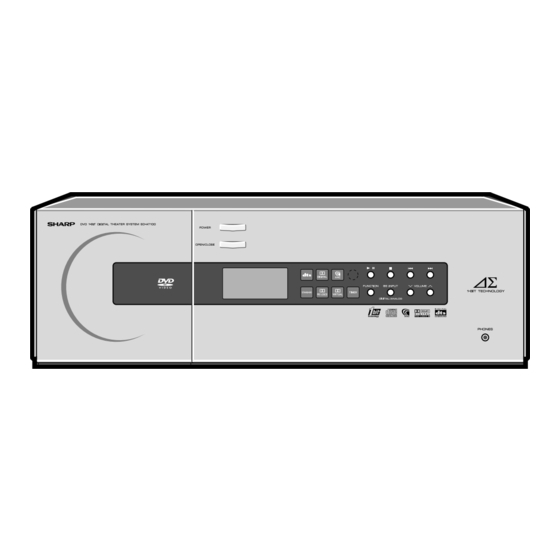
Page 4: Names Of Parts
SD-SH111H NAMES OF PARTS 7 8 9 10 11 12 13 14 15 Front panel 1. Disc Cover 9. DVD Chapter Skip, VCD/CD Track Up or 2. On/Stand-by Button Tuning Up Button 3. Disc Cover Open/Close Button 10. Power Indicator 4. - Page 5 SD-SH111H Rear panel 1. Front Speaker Terminals 2. Centre Speaker Terminals 3. Subwoofer Terminals 4. Surround Speaker Terminals 5. AC Power Input Socket 6. Cooling Fan Rear panel 1. AV2 SCART Socket 7. Aerial Earth Terminal 2. AV1 (TV) SCART Socket 8.
- Page 6 SD-SH111H [Front] Remote control 1. Remote Control Transmitter 2. On/Stand-by Button 3. VCD/CD Play Mode Select Button 4. TV On/Stand-by Button 5. TV Volume Up and Down Buttons 6. TV Input Select Button 7. Tuner (Band) Button 8. Function Buttons 9.
-
Page 7: Disassembly
SD-SH111H DISASSEMBLY Caution on Disassembly Top Panel (C1)x3 Follow the below-mentioned notes when disassembling ø3x8mm the unit and reassembling it, to keep it safe and ensure excellent performance: Top Cabinet 1. Take DVD out of the unit. (B1)x3 2. Be sure to remove the power supply plug from the wall ø3x8mm... - Page 8 SD-SH111H (H1)x1 Front Panel (P1)x1 ø3x6mm (P3)x2 ø3x8mm Washer (J1)x1 (H3)x1 (P1)x1 ø3x8mm ø3x6mm Pull Pull (P1)x1 (P3)x1 ø3x8mm 1-Bit Amp. Shield Cover DVD Mechanism (P1)x1 (P1)x12 ø3x8mm ø3x8mm Washer (P1)x1 ø3x8mm (P1)x4 (H1)x1 Servo PWB ø3x6mm ø3x8mm (P1)x2 (H1)x2 ø3x8mm...
-
Page 9: Removing And Reinstalling The Main Parts
SD-SH111H REMOVING AND REINSTALLING THE MAIN PARTS How to Remove the DVD/CD lid motor (See Figs. 9-1 and 9-2) 1. Remove the front panel. (Refer to the disassembly method on pages 7 and 8.) 2. Remove the screws (A1) x 5 pcs. -
Page 10: Adjustment
SD-SH111H ADJUSTMENT • Adjustment preparation After removing the rear panel, perform adjustment with connectors connected. 1-BIT AMP. PWB 1-BIT AMP. PWB 1-BIT AMP. PWB FROM CNS106A CNS106B CNS106C HEADPHONES PWB CNS504 FROM TO DSP PWB DISPLAY PWB TO DSP PWB... - Page 11 SD-SH111H TUNER SECTION TEST MODE fL: Low-range frequency When the tuner test mode is set, the initial setting of frequencies fC: Middle-range frequency is stored in the preset memory as shown in Table 1. For fH: High-range frequency details, refer to "7. Tuner test" on page 17.
- Page 12 SD-SH111H Notes for handling the mechanism unit Since the pickup semiconductor laser can easily damaged by the static electricity, handle the mechanism unit with care. To prevent damage by the static electricity during transportation, the LD terminals are short-circuited at 2 points on the PWB.
- Page 13 SD-SH111H 1. Shipment Test Mode Outline: Initialization of EEPROM in the DVD unit Function: The unit is set to “Shipment”. (The state immediately after shipment) - All the functions and conditions are initialized. - Clear all of tuner preset memory...
- Page 14 SD-SH111H 2. DVD Test Mode Outline: The key code of the test mode 1 is transmitted to the DVD unit to start up the test mode. Hereafter, the system microcomputer only sends the key code to the DVD unit. Although operations of the main unit can be commenced in the same manner as the DVD/CD functions, nothing has to be controlled except for monitor output.
- Page 15 SD-SH111H Supplementary notes: 1. The DVD/CD cover cannot be opened or closed (loading or unloading discs) in this test mode. After loading a disc, turn the power off to enter this test mode. 2. Operations of keys unrelated to the DVD operations are not accepted except for the POWER key. Therefore, you cannot switch functions, control volume, or control DSP, etc.
- Page 16 SD-SH111H 4. KEY Test Mode Outline: This is to check that the system microcomputer properly acknowledges the key operations on the main unit. Operation: In this test mode, the power is supplied only for the display, and all the FL indications are turned off as in the test menu mode.
- Page 17 SD-SH111H 7. TUNER Test Mode Outline: Start up the unit as set to the TUNER function in the same procedure as the normal operation. Operations and indication after startup are identical with the normal operations. However, what is different is that the frequencies as shown in the table below are set to the tuner preset memory in advance.
- Page 18 SD-SH111H DVD TEST MODE • DVD TEST MODE • DVD ROM RENEWAL MODE (* is a region number) Test mode initial image plane ($ is a TV-TYPE) F0000000 *$&##### (& is a model number) (##### is a program version) <The "1" key of the remote controller is pushed.>...
- Page 19 SD-SH111H From (1) <The "1" key of the remote controller is pushed.> DVD laser lights, the spindle motor Note: Not to face the light of the laser squarely, rotates and the pickup moves to the caution! outer periphery. 30000001 000000DD <The "1"...
- Page 20 SD-SH111H From (2) Following playback, jump test mode "3" Key input PLAY TEST Because a tray opens, adisk is published. 30000001 00000000 "3" Key input PLAY TEST It becomes following play state. DD######********* (******** is a sector ID.)(###### is a error rate)
-
Page 21: Dvd Unit Downlold Procedures
SD-SH111H 1. Version upgrade procedure This unit can overwrite the program inside via the dedicated cable, using the special software from PC. As this program and the program of the drive ass’y need to be matched when replacing the drive ass’y, upgrade the firmware of this unit by following the procedures below. - Page 22 SD-SH111H 8. In a normal end, cut a power supply of the set side after 5. Input "Enter" if heard it with Soft-ware Updata Start? avoiding the tool. = ∗∗∗∗∗∗ Update File 9. Input "ESC" if heard it with Cpntinue / Cancel ? Soft-ware Update Start ? : = ∗∗∗∗∗∗...
-
Page 23: Description Of And How To Avoid Error And Abnormality Indications
SD-SH111H DESCRIPTION OF AND HOW TO AVOID ERROR AND ABNORMALITY INDI- CATIONS Error Cause Preventive measure Press the Open/Close key to open the cover and load a disc. NO DISC • A disc is not loaded. Clean the disc. • The disc cannot be recognized due to scratches Load the disc in a proper direction. -
Page 24: Description Of Circuit For 1-Bit Unit
SD-SH111H DESCRIPTION OF CIRCUIT FOR 1-BIT UNIT (SEE THE WIRING DIAGRAMS ON PAGES 76 AND 77.) Input Signals over certain level input from BIA106 are sliced into waveforms by RA173 (RA174), DA126, and DA127 (DA128, DA129). The slice levels depend on the output of the unit. -
Page 25: To Check And Cancel Protect Circuit Detection Line
SD-SH111H TO CHECK AND CANCEL PROTECT CIRCUIT DETECTION LINE 1. After power supply, the microcomputer (IC301) built in this model consecutively monitors the following errors. If any error occurs, 'Er_AP00' is displayed and all power supply except for the one to drive the microcomputer is interrupted. -
Page 26: Wiring Diagram
SD-SH111H WIRING DIAGRAM FROM FAN MOTOR CNS505 MAIN PWB CNP505 FROM DISPLAY PWB CNP502 CNP503 CNSE02 ROM DOWNLOAD PLUG DSP PWB FROM DVD SERVO PWB CP6001 CNPV02 HEADPHONES PWB CNP308 CNS504 CNP504 CNP506 CNP508 SUBWOOFER CNP101 CNP304 CNP303 CNP301 OUT PWB... - Page 27 SD-SH111H CNSA110B CNSA110D CNSA111C CNSA111B CNSA111A FROM FROM FROM FROM TO MAIN PWB 1-BIT AMP. PWB 1-BIT AMP. PWB 1-BIT AMP. PWB 1-BIT AMP. PWB 1-BIT AMP. PWB CNS306 SPEAKER A PWB CNP706 CNP707 CNP702 CNP703 CNP701 CNP704 CNP705 CNS503...
-
Page 28: Block Diagram
SD-SH111H IC3301 +B10 TA1323F 138 PVDD 5 DAC VDD 144,160 AVDD RF SIGNAL PROCESSOR SERVO 18,23,31,36 CONTROL LDOI LDP1 TR– Q3303 RFRP DIGITAL SERVO RFRP RF RIPPLE CD_LD RPZI CREATION RFZI MDI1 APCI FO– P1DI R-GAIN RFOP RFOP RFCD ADJUST... - Page 29 SD-SH111H +B10 +B10 IC3702 IX0447AW +B10 4M EDO PAGE MODE DRAM VDD3 16,33,59 DAC VDD VDD5 54,74,95 78,89,116 4,160 AVDD 96-104 XVDD 12 106-109,111-113 DDAT0-15 2-5,7-10,31-34,36-39 1,6,20 79-82,84-88 DADR0-8 16-19,22-26 DRAM 92,93 UCAS/LCAS 28,29 90,94 OE/WE 21,35,40 27,13 SYNC DET.
- Page 30 SD-SH111H TO MAIN PWB TO MAIN PWB 10 11 12 13 CNS306 MON_OUT2A VOL_CLK VOL_STB 5 6 7 8 VOL_DATA IC510 – NJM4580M V_SEL1 – OPE AMP. V_SEL2 4 3 2 1 V_SEL3 MON_OUT1A V_SEL4 L_MUTE Q501 Q502 CCB_CE CCB_DI...
- Page 31 SD-SH111H CNW503 CNP503 F_SP_RLY S_SP_RLY C_SP_RLY W_SP_RLY S_MUTE RIMIT –B_CONT PROTECT FAN_L/H +11.5V_RELAY Q504 A_+12V A_–12V OFFSET Q503 Q505 IC502 NJM4580M OPE AMP. CNP504 H.P_R 5 6 7 8 – CNS04 H.P_L – FROM H.P_SW 4 3 2 1 HEADPHONES PWB...
- Page 32 SD-SH111H KDS226 AV1 TV SCART CX07 KDZ10EV QV10 V in V out BLANK QV01 QV02 Ain A QV11 Aout A Ain B Aout B SOV01 QV04 RLY01 QV03 51 50 49 48 47 46 45 44 43 42 41 39 38 37 36 35 34 33...
- Page 33 SD-SH111H +11.5V_RELAY ICV07 NJM7806D VOLTAGE REGULATOR +12V PROTECT DV05 KDS160 SW_GND SW_OUT CHASSIS DV06 KDS160 SOV04 QV21 QV20 ICV02 HC4053FT SWITCH Y-COM X-COM QV09 Z-COM QV17 QV18 4 43 42 41 39 38 37 36 35 34 33 DV01 KDS160...
- Page 34 SD-SH111H D_+2.5V PROTECT DSP_SCCLK DSP_ABOOT _DSP_SCDOUT DSP_INTREQ DSP_SCDOUT DSP_SCDIN _DSP_SCDIN DSP_CS _DSP_INTREQ _DSP_CS W_SP_RLY _DSP_SCCLK DSP_RESET IC101 DSP_UC15 74HC07AF DSP_UC16 BUFFER AMP. DSP_UC17 _DSP_SCDIN 1 44 43 42 41 40 _DSP_SCCLK SPDIF EMAD7 SCCLK EMAD6 AUDATA2 DSP_RESET EMAD5 RESET IC105...
- Page 35 SD-SH111H IC112 D_+3.3V IX0446AW VOLTAGE REGULATOR D_+5V A_+2.5V A_+5V IC111 IX0446AW VOLTAGE REGULATOR IC117 MX27L212 EPROM /EXTMEM Q105 IC115 EMAD7 IC114 TVHC574T EMAD6 TVHC574T LATCH DSP_UC17 EMAD5 LATCH EMAD4 EMAD0 EMAD3 EMAD1 EMAD2 DSP_UC16 EMAD2 EMAD3 DSP_UC15 EMAD1 EMAD4 EMAD0...
- Page 36 SD-SH111H +3.3V(USWD) +3.3V(SWD) Q301 Q306 C_SP_RLY F_SP_RLY POWER_KEY TU_MUTE CCB_DO CCB_CL CCB_DI CCB_CE TUNER_SM SD_ST_IN IC301 PROTECT IX0547AW AREA SYSTEM MICROCOMPUTER TV_TYPE DOOR_PROT KEY2 AVSS KEY1 A/D_RESET VREF POWER AVCC POSISTOR F_CONT 9 10 11 12 13 14 15 16 17 18 19 20 21 22 23 24 25 26 27 28 29 30...
- Page 37 SD-SH111H Q304 IC302 DVD/CD LID MOTOR TA7291F MOTOR DRIVER M– 8 10 12 14 16 IC304 CNP303 CNS303 74VHCT08 GATE IC OPEN/CLOSE DOOR_OP DOOR_CL D_M+ D_M– CNP304 CNS304 M– CNP306 VOL_CLK VOL_STB VOL_DATA PROTECT DIG_FUNC+B V_SEL1 V-MODE DSP_INTREQ V_SEL2 ASPECT...
- Page 38 SD-SH111H FLE01 1 2 3 4 5 6 7 8 9 10 11 12 13 14 15 16 17 18 19 20 21 22 23 24 25 26 27 28 29 30 31 32 33 34 35 36 37 38 39 40 41 42 43 44 45 46 47 48 49 50 51 52 53 54 5...
- Page 39 SD-SH111H SPEAKER A CNP714 ICE03 KIA7805AP CONSTANT VOLTAGE +13V REGULATOR 9 50 51 52 53 54 55 56 57 58 59 60 61 62 63 64 65 66 67 68 69 70 71 72 73 74 75 76 77 78 79 80 81 82 83 84...
- Page 40 SD-SH111H IC921 NJM2370R VOLTAGE REGULATOR Vout Q921 CONT NOISE BYPASS IC924 NJM431L PS924 VOLTAGE REGULATOR D939 CNP907 +3.7V STAND-BY D_GND POWER_ POWER Q927 POSISTOR GND(M1) +11.5V RELAY FREQ L950 D937 D936 CNP908 EK16 EK16 D934 D935 EK16 EK16 Q928 L923...
- Page 41 SD-SH111H T901 SUB POWER PS921 TRANSFORMER THERMISTOR IC926 TA78DL12AF D931 S1VBA60 VOLTAGE REGULATOR ZD924 DZ270BSA Q905 PC902 TLP621 IC923 PC901 SE012N TLP621 ERROR DETECTION AMP. L921 4.7µH D921 DX0522CE CNS902 BI902 +13V C906 0.0033 D902 D903 ZD901 SFPL52V SFPL52V DZ10BSB...
- Page 42 SD-SH111H FROM DISPLAY PWB CNSE07 CNP714 FROM +13V POWER A PWB CNS902 –13V CNP704 CNS503 F_SP_RLY RL701 S_SP_RLY C_SP_RLY W_SP_RLY Q701 RIMIT –B_CONT PROTECT FAN_L/H +11V_RELAY A+12V A-12V OFFSET FR_P FRONT_RCH+ FR_M FRONT_RCH– FL_M FRONT_LCH– FL_P FRONT_LCH+ RL702 FROM 1-BIT AMP.PWB...
- Page 43 SD-SH111H CNP701 +B_AMP FROM 1-BIT AMP. PWB –B_AMP CNSA111C –B_DRIVER AMP_VCC CNP702 +B_AMP FROM 1-BIT AMP. PWB –B_AMP CNSA111B –B_DRIVER AMP_VCC CNP703 +B_AMP FROM 1-BIT AMP. PWB –B_AMP CNSA111A –B_DRIVER AMP_VCC IC702 KIA7806AP CONSTANT VOLTAGE REGULATOR Q718 Q712 – Q713 –...
- Page 44 SD-SH111H SLICE LEVEL SET VOLTAGE DEAD TIME CONTROL POWER - OUTPUT OFFSET ADJUSTMENT ICA100 IX0498AW 7TH ORDER ∆∑ MODULATION CONVERSION LSI QA101 QA102 LOW PASS FILTER SYSTEM MICROCOMPUTER LOAD Figure 44 BLOCK DIAGRAM (17/17) – 44 –...
-
Page 45: Wiring Side Of P.w.board / Schematic Diagram
SD-SH111H SPINDLE MOTOR SLED MOTOR – – FLEXBLE PWB DVD PICKUP P60 3 - H UNIT CS3301 DVD SERVO PWB DVD MOTOR PWB-H COLOR TABLE BROWN R D ( R ) ORANGE YELLOW GREEN BLUE VIOLET FAN MOTOR GRAY W H ( W ) - Page 46 SD-SH111H MAIN PWB-A (TOP VIEW) C579 C583 C575 C577 CNP502 C573 CNP503 P48 3 - A C581 CNSE02 FROM P54 3 - A DISPLAY PWB CNS503 TO SPEAKER A PWB HEADPHONES C574 PWB-B2 (TOP VIEW) P51 7 - C RLY01...
- Page 47 SD-SH111H P45 5 - G FROM FAN MOTOR CNS505 MAIN PWB-A (BOTTOM VIEW) CNP505 TP5030 C567 3 2 1 TP5029 Q525 TP5052 TP5051 TP5028 Q526 TP5027 TP50314 C566 IC509 TP50315 TP5026 D522 COLOR TABLE TP50313 TP5025 D521 C572 TP50311 BROWN...
- Page 48 SD-SH111H P52 1 - E TO POWER B PWB P46 5 - A P52 1 - B TO MAIN PWB TO POWER B PWB CNP908 CNP907 CNP502 CNSE06 1 2 3 4 5 6 7 8 9 10 11 12...
- Page 49 SD-SH111H P60 1 - C TO DVD SERVO PWB CP3201 CNSE01 ICE02 LE01 BIE01 BIE05A LE03 RF49 SWE01 ON/STAND-BY BIE05B RF32 SWE06 CE12 OPEN/CLOSE RF33 LE02 RF48 CE07 ICE05 ZDE01 RF31 CE04 CE10 QE13 CE01 QE06 QE05 QE04 SWE02 PLAY...
- Page 50 SD-SH111H DSP PWB-C (TOP VIEW) C144 C157 R152 R151 C205 D309 IC109 C110 R159 R157 R209 R208 R211 C195 R123 R174 R212 R112 R213 C178 C101 R175 R173 R176 IC102 C107 R178 R177 R179 R180 R184 R182 R181 R110 C126...
- Page 51 SD-SH111H • Through-hole where the top, bottom and +B patterns are connected. • Through-hole where the top, bottom and ground patterns are connected. • Through-hole where the top, and bottom patterns are connected. DSP PWB-C (BOTTOM VIEW) C165 C166 C167...
- Page 52 SD-SH111H POWER A PWB-D1 (TOP VIEW) L902 LG901 VA901 When Servicing, pay attention as the F901 area enclosed by this line ( ) is T2.5A L 250V directly connected with AC main voltage. SO900 RZ903 AC INLET RZ904 AC 230 V, 50 Hz...
- Page 53 SD-SH111H POWER A PWB-D1 (BOTTOM VIEW) POWER B PWB-D2 (BOTTOM VIEW) COLOR TABLE BROWN RD(R) ORANGE YELLOW GREEN BLUE VIOLET GRAY WH(W) WHITE BLACK PINK POWER C PWB-D3 (BOTTOM VIEW) Figure 53 WIRING SIDE OF P.W.BOARD (9/17) – 53 –...
- Page 54 SD-SH111H P46 2 - B TO MAIN PWB CNP503 P52 6 - G FROM POWER A PWB CNS902 C713 3 5 7 9 111315 2 4 6 8 101214 D736 C712 CNS503 D735 RL701 RL705 D734 R707 R701 Q704 Q718...
- Page 55 SD-SH111H SPEAKER B PWB-E2 (BOTTOM VIEW) SPEAKER A PWB-E1 (BOTTOM VIEW) Figure 55 WIRING SIDE OF P.W.BOARD (11/17) – 55 –...
- Page 56 SD-SH111H P46 6 - F TO MAIN PWB CNW508B CNSA106A 1-BIT AMP. PWB-F1 (TOP VIEW) R-CH OUTPUT OFFSET ADJUSTMENT CA186 BIA106A CA196 CXA100 VRA101 RA174 RA173 CA288 RA183 RA184 RA103 CA102 CA212 CA164 CA105 CA185 CA189 CA188 RA181 VRA100 CA187...
- Page 57 SD-SH111H • Through-hole where the top, bottom and +B patterns are connected. • Through-hole where the top, bottom and ground patterns are connected. • Through-hole where the top, and bottom patterns are connected. 1-BIT AMP. PWB-F1~3 (BOTTOM VIEW) RA100 RA101...
- Page 58 SD-SH111H P46 6 - F TO MAIN PWB CNW508C CNSA106B 1-BIT AMP. PWB-F2 (TOP VIEW) R-CH OUTPUT OFFSET ADJUSTMENT BIA106B CA196 CA186 CXA100 VRA101 RA173 RA174 CA288 RA183 RA184 RA103 CA102 CA164 CA212 CA105 CA185 CA189 CA188 RA181 VRA100 CA187...
- Page 59 SD-SH111H • Through-hole where the top, bottom and +B patterns are connected. • Through-hole where the top, bottom and ground patterns are connected. • Through-hole where the top, and bottom patterns are connected. P46 6 - G TO MAIN PWB...
- Page 60 SD-SH111H P46 2 - B TO MAIN PWB CNV01 DVD SERVO PWB-G (TOP VIEW) CP5001 IC3662 C3670 C5022 C5021 C5035 C5023 IC3661 R5028 R5026 CP3201 C5020 C5019 C5108 C5034 R5080 R5023 R5021 R5019 C3669 R5078 R5077 Q5005 Q5004 Q5014 C3668...
- Page 61 SD-SH111H • Through-hole where the top, bottom and +B patterns are connected. • Through-hole where the top, bottom and ground patterns are connected. • Through-hole where the top, and bottom patterns are connected. DVD SERVO PWB-G (BOTTOM VIEW) R5041 R5042...
- Page 62 SD-SH111H P65 9 - H/P65 12 - G TO MAIN PWB 10 11 12 13 R653 C617 C605 100P C607 CNS306 (CH) 10/16 10/16 MON_OUT2A VOL_CLK R639 C623 R657 R508 R510 VOL_STB 5 6 7 8 VOL_DATA R646 C517 –...
- Page 63 SD-SH111H F_SP_RLY S_SP_RLY C_SP_RLY W_SP_RLY S_MUTE RIMIT –B_CONT PROTECT R510 FAN_L/H R523 +11.5V_RELAY C517 100/10 GND_M R647 A_+12V A_GND(A) R516 C611 1.5K A_–12V R512 100/10 470K OFFSET R522 470K Q503 KTA1504 GR R535 C537 C535 10/16 R514 R531 R659 (CH)
- Page 64 SD-SH111H KDS226 CV90 0.22 SOV01 CV91 RV40 CX07 AV1 TV SCART SOV01 0.22 KDZ10EV SCART TERMINAL V in V out QV10 RV37 BLANK KTC4375 Y RV36 RV30 RV32 RV80 Ain A RV11 QV11 Aout A RV33 RV31 Ain B KTC4375 Y...
- Page 65 SD-SH111H VIDEO OUT SIGNAL VIDEO IN SIGNAL +11.5V_RELAY ICV07 NJM7806D VOLTAGE REGULATOR RV63 +12V QV20 A_GND KTC4375 Y PROTECT DV05 KDS160 SW_GND CV83 CV82 SW_OUT QV21 KTC4375 Y RV64 CHASSIS DV06 CX06 KDS160 0.001 RV38 RV39 CX04 0.001 CV96 100/16...
- Page 66 SD-SH111H DISPLAY PWB-B1 FLE01 1 2 3 4 5 6 7 8 9 10 11 12 13 14 15 16 17 18 19 20 21 22 23 24 25 26 27 28 29 30 31 32 33 34 35 36 37 38 39 40 41 42 43 44 45 46 47 48 49 50 51 52 53 54 55 56...
- Page 67 SD-SH111H P74 2 - A TO SPEAKER A PWB CNP714 CNSE07 ICE03, ICE04 KIA7805AP BIE07 CONSTANT VOLTAGE +13V CNPE01 REGULATOR A+5V RF46 DE05 KDS160 P76 1 - C D+5V CNSA112D ICE03 7 48 49 50 51 52 53 54 55 56 57 58 59 60 61 62 63 64 65 66 67 68 69 70 71 72 73 74 75 76 77 78 79 80 81 82 83 84 FROM 1-BIT AMP.
- Page 68 SD-SH111H FM SIGNAL D_+2.5V D101 KDS160 R190 R191 D102 KDS160 PROTECT DSP_SCCLK DSP_ABOOT _DSP_SCDOUT C109 10/16 DSP_INTREQ DSP_SCDOUT DSP_SCDIN _DSP_SCDIN C110 0.022 C125 DSP_CS _DSP_INTREQ _DSP_CS R195 4.7K W_SP_RLY _DSP_SCCLK DSP_RESET IC101 DSP_UC15 74HC07AF DSP_UC16 BUFFER AMP. C159 DSP_UC17 _DSP_SCDIN...
- Page 69 SD-SH111H IC112 D_+3.3V IX0446AW D_GND(3) VOLTAGE REGULATOR D_+5V C148 47/16 C140 C151 D101 C136 47/16 KDS160 D_GND R190 A_+2.5V A_+5V IC111 C199 R191 D102 C198 C196 C197 47/16 KDS160 IX0446AW 47/16 A_GND VOLTAGE REGULATOR IC117 MX27L212 EPROM /EXTMEM Q105 R110...
- Page 70 SD-SH111H +3.3V(USWD) R405 R411 Q301 +3.3V(SWD) R453 KRC107 S R410 R449 C308 C334 0.001 47P(CH) C441 R448 Q306 22/16 KRA106 S C_SP_RLY R375 R399 F_SP_RLY R376 POWER_KEY R377 TU_MUTE R378 R398 CCB_DO R379 CCB_CL R380 CCB_DI R381 CCB_CE R382 D308...
- Page 71 SD-SH111H R435 2.2K Q304 R411 KRC107 S IC302 DVD/CD LID CNP303 CNS303 MOTOR TA7291F C321 10/16 MOTOR DRIVER M– IC304 8 10 12 14 16 74VHCT08 GATE IC C334 OPEN/CLOSE 47P(CH) CNP304 CNS304 DOOR_OP R419 1.5K DOOR_CL D_M+ D_M– M–...
- Page 72 SD-SH111H POWRE B PWB-D2 CNS905 IC921 NJM2370R VOLTAGE REGULATOR IC924 NJM431L Vout R969 Q921 VOLTAGE REGULATOR 1.5K KTD2058 Y R971 CONT R925 NOISE C927 BYPASS 0.001 R981 R924 C943 C926 10/16 C942 47/25 C969 PS924 R926 POSISTOR D939 R980 1N4004S CNP907 +3.7V...
- Page 73 SD-SH111H POWER C PWB-D3 T901 SUB POWER CNP904 CNS904 TRANSFORMER PS921 THERMISTOR IC926 TA78D12F D931 VOLTAGE REGULATOR S1VBA60 C963 0.047 (ML) C964 0.047 ZD924 R972 (ML) DZ27BSA 2.7K R973 C971 C972 C941 R979 R978 100/25 470/35 4.7K 4.7K R974 PC902...
- Page 74 SD-SH111H P67 10 - A FROM DISPLAY PWB CNSE07 CNP714 CNP704 +13V P72 6 - E GND(D1) CNS902 FROM –13V –B D731 –B POWER A PWB KDS160 D734 –B SFPW56 CNS503 F_SP_RLY FM SIGNAL RL701 S_SP_RLY C_SP_RLY Q701 R810 KTC3875 GR...
- Page 75 SD-SH111H CNP701 R743 0.11 C755 +B_AMP 0.01 R744 P77 12 - F 0.11 C756 –B_AMP CNSA111C 0.01 –B_DRIVER –B FROM 1-BIT AMP. PWB C757 AMP_VCC C758 0.01 0.01 –B R745 CNP702 0.11 C747 +B_AMP 0.01 R746 P77 12 - F 0.11...
- Page 76 SD-SH111H 1-BIT AMP. PWB-F1/2/3 FM SIGNAL BIA106A/B/C R-CH_IN R_CH AGND L-CH_IN CA211 CA288 LFA01 ICA110 A+5V A+5V TC74AC8T AGND_AD QUAD 2 INPUT AND G LFA02 D+5V D+5V RA124 DA103 KDS160 CA155 CA197 DGND_AD 12P(CH) 47/25 RA115 2.2K DA102 RESET CA289...
- Page 77 SD-SH111H ICA106, ICA107 SLA5505M SWITCHING AUDIO POWER AMP. DA252 SFPW56 LA130 LA100 DA251 CA280 SFPW56 CA142 CA177 CA278 CA250 0.01 CA178 CA251 CA143 0.01 0.001 10 11 12 13 14 15 16 17 18 LA131 CA256 CA254 0.001 0.001 CA110...
- Page 78 SD-SH111H DVD SERVO PWB-G (1/3) Q3301 FB3301 KTA1504 Y 10µH R3310 4.7K C3307 C3319 100/6.3 47/6.3 Q3307 D3301 C3333 C3306 C3312 KRC104 S R3303 DAP202K 0.001 0.01 0.01 2.2K 3 2 1 R3315 R3320 R3739 C3332 4.7K 0.001 R3344 R3343...
- Page 79 SD-SH111H 40 39 38 37 36 35 34 33 32 31 30 29 28 27 26 25 24 23 22 21 IC3702 IX0447AW 4M EDO C3752 PAGE MODE RAM 1 2 3 4 5 6 7 8 9 10 11...
- Page 80 SD-SH111H R3518 FL3501 20MHz R3517 R3522 R3543 10K HGA_CS C3602 C3603 100/6.3 Q3503 R3513 C3604 KRC104 S 4.7K C3510 90 89 88 87 86 85 84 83 82 81 80 79 78 77 76 75 74 73 72 71 70 69 68 67 66 65 64 63 62 61 R3544 4.7K...
- Page 81 SD-SH111H DVD SERVO PWB-G (2/3) C3631 47/6.3 C3629 100/6.3 L3602 47µH FB3605 100mA C3627 10P(CH) 158 157 156 155 154 153 152 151 150 149 148 147 146 145 144 143 142 141 140 139 138 137 136 135 134 133 132 131 130 129 128 127 126 125 124 123 122 121...
- Page 82 SD-SH111H DVD SERVO PWB-G (3/3) C5003 C5006 C5012 C5018 68P(CH) 27P(CH) 39P(CH) R5010 (CH) L5005 3.9K 27µH R5016 R5004 L5002 R5007 27µH Q5004 R5019 2SC2412 KR C5009 Q5001 5P(CH) R5013 R5020 KTA1504 Y C5004 C5007 C5013 C5019 27P(CH) 68P(CH) (CH)
- Page 83 SD-SH111H VIDEO OUT SIGNAL C5018 R5031 (CH) R5025 6.8K 1.2K Q5010 5016 2SC2412 KR Q5007 2SC2412 KR C5021 R5019 47/6.3 L5009 R5032 R5040 CP5001 100mA 3.3K R5020 L5010 SPDIF_O R5026 D_GND L5008 C5019 D_5V 7P(CH) R5027 R5033 100mA A_GND 6.8K 1.2K...
- Page 84 SD-SH111H DVD MOTOR PWB-H TR– TR– FO– FO– PICKUP UNIT VOSC VOSC FLEXBLE LD– LD– DISC1_SW CAM_SW LD/EJ_SW SPINDLE MOTOR – SP– SP– IN_SW PICKUP IN SL– – SL– SLED MOTOR • NOTES ON SCHEMATIC DIAGRAM can be found on page 86.
-
Page 85: Voltage
SD-SH111H VOLTAGE IC3701 IC3601 IC3504 IC3801 IC3603 IC3508 NO. VOLTAGE NO. VOLTAGE NO. VOLTAGE NO. VOLTAGE NO. VOLTAGE NO. VOLTAGE NO. VOLTAGE NO. VOLTAGE NO. VOLTAGE NO. VOLTAGE NO. VOLTAGE 1.6 V 3.3 V 2.5 V 3.3 V 3.3 V 3.3 V... -
Page 86: Notes On Schematic Diagram
SD-SH111H NOTES ON SCHEMATIC DIAGRAM • The indicated voltage in each section is the one measured • Resistor: by Digital Multimeter between such a section and the chas- To differentiate the units of resistors, such symbol as K and M are used: the symbol K means 1000 ohm and the symbol sis with no signal given. -
Page 87: Waveforms Of 1-Bit Circuit
SD-SH111H WAVEFORMS OF 1-BIT CIRCUIT 2.00V/div 2.00V/div 2.00V/div 2.00V/div AD IC Output + Side LEVEL SHIFT OUT DEAD TIME - Side 500ns/div 194.545465µs 520mV 50.0ns/div 0.0s -12.30V Amplitude Dead time is generated by level from 0 to 5 V ZOOM UP shift input. -
Page 88: Waveforms Of Dvd Circuit
SD-SH111H WAVEFORMS OF DVD CIRCUIT – 88 –... -
Page 89: Troubleshooting
SD-SH111H TROUBLESHOOTING Repair the changer mechanism. The disc does not rotate. Is the disc chucked at the specified location ? Check the changer mechanism. Check the connection between pins 3 and 7 of IC705 and M3. Replace IC705. Check the cable connecting to the CS3301. - Page 90 SD-SH111H The [No Disc] indication. (In case focus servo does not function.) Is the focus control signal output to the pin 14 of Check the IC3701 DAC power source periphery IC3701? circuit. If it is normal, replace IC3701. Is the focus control signal from the pin 158 of...
- Page 91 SD-SH111H Both picture and sound do not operate normally. (1) Place the disc on the tray and close it. When chucked, disc starts rotating ? Refer to “Disc does not turn.” Is the level of RF signal which is output from Check for contamination of objective lens of optical pickup.
-
Page 92: Function Table Of Ic
SD-SH111H FUNCTION TABLE OF IC IC3701 VHiTC94A03F-1: Servo ECC (TC94A03F) (1/3) Terminal Name Input/Output Pin No. Function ASLCN Output Data slice negative output. ASLCO Output Analog data slice output. (at differential input, digital slice output enable) DVSS — DAC ground. - Page 93 SD-SH111H IC3701 VHiTC94A03F-1: Servo ECC (TC94A03F) (2/3) Terminal Name Input/Output Function Pin No. TESM4 — Test terminal. VDD3 Input 3.3 V digital power supply. 79-82 BA0-4 Output External RAM address output. VSS5 — 5 V ground. 84-88 BA4-8 Output External RAM address output.
- Page 94 SD-SH111H IC3701 VHiTC94A03F-1: Servo ECC (TC94A03F) (3/3) Terminal Name Input/Output Function Pin No. RFRP Input RFRP signal input. AVSS Input Power supply for 3.3 V analog system. TESM10 — Test terminal. EXTAD Input General-purpose external ADC input. VREF Input Reference power supply for analog system: 1.65 V.
- Page 95 SD-SH111H IC3301 VHiTA1323F+-1: RF Signal Processor (TA1323F) (1/2) Pin No. Terminal Name Input/Output Function — GND terminal. P2TP Input TE+ input. (CD) P2TN Input TE– input. (CD) LDO2 Output Drive output 2. MDI2 Input Monitor input 2. Output Digital VREF.
- Page 96 SD-SH111H IC3301 VHiTA1323F+-1: RF Signal Processor (TA1323F) (2/2) Pin No. Terminal Name Input/Output Function P1CI Input C input. (DVD) P1BI Input B input. (DVD) P1AI Input A input. (DVD) GNDR — GND terminal. (RF) LDP2 Input APC polarity 2. P2AI Input A input.
- Page 97 SD-SH111H IC3508 RH-iX1761GEZZ: Track Buffer Interface (IX1761GE) (1/2) Pin No. Terminal Name Input/Output Function VDD1 Input Digital power supply +3.3 V. HADR0 Input CPU Address bus. HADR1 Input CPU Address bus. HADR2 Input CPU Address bus. HADR3 Input CPU Address bus.
- Page 98 SD-SH111H IC3508 RH-iX1761GEZZ: Track Buffer Interface (IX1761GE) (2/2) Pin No. Terminal Name Input/Output Function VDD1 Input Digital power supply +3.3 V. 5VBUFO[B] Output 5 V buffer output B. 5VBUFI[B] Output 5 V buffer input B. (3.3 V input) 5VBUFO[A] Output 5 V buffer output A.
- Page 99 SD-SH111H IC3801 VHiBA5984FP-1: Motor Driver (BA5984FP) Pin No. Terminal Name Function LD-FWD Loading driver FWD input terminal. SL_IN(+) CH 1 Former stage amplifier nonreverse input terminal. SL_IN(-) CH 1 Former stage amplifier reverse input terminal. SLOUT CH 1 Former stage amplifier output terminal.
- Page 100 SD-SH111H IC3504 RH-iX1687GEZZ: DVD Microcomputer (IX1687GE) Port D Port E PA7/A23/IRO7 EXTAL PA6/A22/IRO6 XTAL PA5/A21/IRO5 STBY PA4/A20/IRO4 PA3/A19 WOTOVF(FWE)* PA2/A18 PA1/A17 H8S/2000 CPU PA0/A16 PB7/A15 PB6/A14 PB5/A13 PB4/A12 Interruption controller PB3/A11 PA2/A10 PB1/A9 PB0/A8 PF7/ø PF6/AS DMAC PF5/RD RAM* PC7/A7...
- Page 101 SD-SH111H ICA100 RH-iX0498AWZZ: 7th Order Modulation Conversion LSI (IX0498AW) Pin No. Function Port Name Input/Output VDDL Input L channel digital output section power terminal OUTL (+) Output L channel forward output terminal OUTL (–) Output L channel reverse output terminal GNDD —...
-
Page 102: Fl Display
SD-SH111H FL DISPLAY FLE01 VVKHNA15LS+-1: FL Display SLEEP DISC PROGRSM RANDOM RT TP TA PTYI EON PTY TI STEREO TRACK TITLE TOTAL CHAPTER ANGLE ( 1G-8G, 11G-15G ) ANODE CONNECTION 1G–8G, 12G,14G 1G–8G, 12G,14G 1 –1 DISC 1 –5 1–1 1–1... - Page 103 “HOW TO ORDER REPLACEMENT PARTS” To have your order filled promptly and correctly, please furnish the For U.S.A. only following information. Contact your nearest SHARP Parts Distributor to order. 1. MODEL NUMBER 2. REF. No. 3. PART NO. 4. DESCRIPTION For location of SHARP Parts Distributor, Please call Toll-Free;...
- Page 104 SD-SH111H PRICE PRICE PART CODE DESCRIPTION PARTS CODE DESCRIPTION RANK RANK TRANSISTORS INTEGRATED CIRCUITS Q101 VSKRA107S//-1 AB Digital,NPN,KRA107 S IC101 VHI74HC07AF-1 AF Buffer Amp.,74HC07AF Q102 VSKRC107S//-1 AB Digital,NPN,KRC107 S IC102 VHIAK4586VQ-1 BC ADC/DAC/DIR Converter, Q103 VSKRA107S//-1 AB Digital,NPN,KRA107 S AK4586VQ...
- Page 105 SD-SH111H PRICE PRICE DESCRIPTION DESCRIPTION PART CODE PARTS CODE RANK RANK 1 L903 DIODES RCILZ0045AWZZ AU AC Line Filter AG Coil,4.7 µH L921,922 RCILZ0043AWZZ AG Coil,100 µH L923,924 RCILZ0044AWZZ D101~104 VHDKDS160//-1 AB Silicon,KDS160 L950 RCILZ0047AWZZ AG Coil D301~311 VHDKDS160//-1 AB Silicon,KDS160 AC 10 µH...
- Page 106 SD-SH111H PRICE PRICE PART CODE DESCRIPTION PARTS CODE DESCRIPTION RANK RANK AB 10 µF,16V,Electrolytic AB 10 µF,16V,Electrolytic C141 VCEAPS106AF1C C519~527 VCEAPS106AF1C AB 0.022 µF,25V AC 100 µF,16V,Electrolytic C142 VCKYCY1EF223Z C528 VCEAPS107AF1C AA 0.001 µF,50V AB 10 µF,16V,Electrolytic C143 VCKYCY1HB102K J...
- Page 107 SD-SH111H PRICE PRICE DESCRIPTION DESCRIPTION PART CODE PARTS CODE RANK RANK AF 0.0047 µF,400V AB 0.1 µF,16V 1 C920 RC-KZ0010AWZZ C3618,3619 VCKYCY1CB104K J AL 5600 µF,16V,Electrolytic AC 100 µF,6.3V,Electrolytic C921 RC-EZ0068AWZZ C3620 VCEAPS107AF0J AA 0.01 µF,50V AB 0.1 µF,16V C924...
- Page 108 SD-SH111H PRICE PRICE PART CODE DESCRIPTION PARTS CODE DESCRIPTION RANK RANK AF 10 µF,10V,Electrolytic AB 10 µF,16V,Electrolytic CA105,106 RC-EZ0007AWZZ CT05 VCEAPS106AF1C AA 0.1 µF,25V AB 0.022 µF,25V CA107 VCKYCY1EF104Z CT06~08 VCKYCY1EF223Z AC 10 µF,10V,Electrolytic AD 47 µF,10V,Electrolytic CA108,109 RC-EZ0051AWZZ CT09 VCEAPS476AF1A AA 0.1 µF,25V...
- Page 109 SD-SH111H PRICE PRICE DESCRIPTION DESCRIPTION PART CODE PARTS CODE RANK RANK R164,165 VRS-CY1JB273J AA 27 kohms,1/16W R521 VRS-CY1JB561J AA 560 ohms,1/16W R166,167 VRS-CY1JB561J AA 560 ohms,1/16W R522 VRS-CY1JB474J AA 470 kohms,1/16W R168,169 VRS-CY1JB104J AA 100 kohm,1/16W R523 VRS-TW2EE221J AA 220 ohms,1/4W...
- Page 110 SD-SH111H PRICE PRICE PART CODE DESCRIPTION PARTS CODE DESCRIPTION RANK RANK R659,660 VRS-TW2EE750J AC 75 ohms,1/4W R932 VRS-TQ2BB222J AA 2.2 kohms,1/8W R661 VRS-CY1JB104J AA 100 kohm,1/16W R933 VRS-TW2EE101J AC 100 ohms,1/4W R674 VRS-CY1JB152J AA 1.5 kohms,1/16W R934 VRS-CY1JB333D AA 33 kohms,1/16W...
- Page 111 SD-SH111H PRICE PRICE DESCRIPTION DESCRIPTION PART CODE PARTS CODE RANK RANK R3531 VRS-CY1JB472J AA 4.7 kohms,1/16W R5016~5018 VRS-CY1JB102J AA 1 kohm,1/16W R3532~3535 VRS-CY1JB103J AA 10 kohm,1/16W R5019 VRS-CY1JB821J AA 820 ohms,1/16W R3537,3538 VRS-CY1JB103J AA 10 kohm,1/16W R5020 VRS-CY1JB471J AA 470 ohms,1/16W...
- Page 112 SD-SH111H PRICE PRICE PART CODE DESCRIPTION PARTS CODE DESCRIPTION RANK RANK 1 RZ905 RF33 VRS-CY1JB223J AA 22 kohms,1/16W VRS-TW2EE154J AC 150 kohms,1/4W RF34 VRS-TV2AB821J AA 820 ohms,1/10W RZ906 VRS-CY1JB242D AB 2.4 kohms,1/16W RF35,36 VRS-TV2AB102J AA 1 kohm,1/10W RZ907 VRS-CY1JB122D AA 1.2 kohms,1/16W...
- Page 113 SD-SH111H PRICE PRICE DESCRIPTION DESCRIPTION PART CODE PARTS CODE RANK RANK K1,2 QLUGP0002AWZZ J AB Lug PFLT-0059AWZZ AD Felt,Stabilizer ———— Motor with Chassis [Spindle] PFLT-0061AWZZ AB Felt,Tray ———— Motor with Gear [Sled] PFLT-0062AWZZ AB Felt,Adaptor RMOTV0043AWZZ J AN DVD/CD Lid Motor...
- Page 114 SD-SH111H PRICE PART CODE DESCRIPTION RANK SPAKC1483AWZZ J Packing Case SSAKH0076AWZZ J AD Polyethylene Bag,Unit TINSZ0830AWZZ AR Operation Manual TCAUZ0133AWZZ J AB Sheet,Heat Caution 92LBAG1770A AB Polyethylene Bag,AC Power Supply Cord QANTL0012AWZZ J AS AM Loop Antenna TCADS0004AWZZ J AD Card,Service...
- Page 115 SD-SH111H 603x3 603x18 603x2 603x3 TUNER UNIT 603x3 623x2 603x2 607x3 603x2 277x4 PWB-A Silicon Grease 603x2 271-4 612x2 602x2 271-11 PWB-C 271-10 PWB-E1 IC702 271-9 271-3 606x2 271-6 PWB-E2 271-2 607x2 271-1 271-5 271-8 612x12 605x2 271-7 610x2 612x2...
- Page 116 SD-SH111H © COPYRIGHT 2002 BY SHARP CORPORATION ALL RIGHTS RESERVED. No part of this publication may be reproduced, stored in a retrieval system, or transmitted in any form or by any means, electronic, mechanical, photocopying, recording, or otherwise, without prior written permission of the publisher.