Sony XAV-AX100 Service Manual
Hide thumbs
Also See for XAV-AX100:
- Operating instructions manual (33 pages) ,
- Operating instructions manual (116 pages) ,
- Operating instructions manual (84 pages)
Table of Contents
Advertisement
Quick Links
2018/04/20 05:03:25 (GMT+09:00)
XAV-AX100/AX100C2
SERVICE MANUAL
Ver. 1.3 2018.03
• This model is not equipped with a mechanism deck.
(US, CND models)
FOR THE CUSTOMERS IN THE USA. NOT
APPLICABLE IN CANADA, INCLUDING IN THE
PROVINCE OF QUEBEC.
POUR LES CLIENTS AUX ÉTATS-UNIS. NON
APPLICABLE AU CANADA, Y COMPRIS LA
PROVINCE DE QUÉBEC.
AUDIO POWER SPECIFICATIONS
CTA Standard
Power Output: 20 Watts RMS × 4 at 4
Ohms < 1% THD+N
SN Ratio: 80 dBA (reference: 1 Watt into
4 Ohms)
Monitor section
Display type: Wide LCD color monitor
Dimensions: 6.4 in
System: TFT active matrix
Number of pixels:
1,152,000 pixels (800 × 3 (RGB) × 480)
Color system:
PAL/NTSC/SECAM/PAL-M automatic select for
CAMERA IN terminal
Tuner section
FM
(US, CND
models
)
Tuning range: 87.5 – 107.9 MHz
models
(AEP, UK, IND, IND3
Tuning range: 87.5 – 108.0 MHz
(E
model
)
Tuning range:
87.5 - 108.0 MHz (at 50 kHz step)
87.5 – 108.0 MHz (at 100 kHz step)
87.5 – 107.9 MHz (at 200 kHz step)
FM tuning step:
50 kHz/100 kHz/200 kHz switchable
9-896-336-04
2018C33-1
©
2018.03
Antenna (aerial) terminal:
External antenna (aerial) connector
Intermediate frequency: 150 kHz
Usable sensitivity: 10 dBf
Selectivity: 70 dB at 400 kHz
Signal-to-noise ratio: 70 dB (mono)
Separation at 1 kHz: 30 dB
Frequency response: 20 – 15,000 Hz
AM
models
(US, CND
)
Tuning range: 530 – 1,710 kHz
Antenna (aerial) terminal:
External antenna (aerial) connector
Intermediate frequency:
9,267.5 kHz or 9,257.5 kHz/5 kHz
Sensitivity: 44 μV
(AEP, UK, IND, IND3
models
Tuning range: 531 – 1,602 kHz
Antenna (aerial) terminal:
External antenna (aerial) connector
Intermediate frequency:
9,267 kHz or 9,258 kHz/4.5 kHz
Sensitivity: 44 μV
(E
model
)
Tuning range:
531 - 1,602 kHz (at 9 kHz step)
530 - 1,710 kHz (at 10 kHz step)
AM tuning step:
)
9 kHz/10 kHz switchable
Antenna (aerial) terminal:
External antenna (aerial) connector
Intermediate frequency:
9,267 kHz or 9,258 kHz/4.5 kHz (at 9 kHz step)
9,267.5 kHz or 9,257.5 kHz/5 kHz (at 10 kHz step)
Sensitivity: 44 μV
USB player section
Interface: USB (High-speed)
Maximum current: 1.5 A
Sony Video & Sound Products Inc.
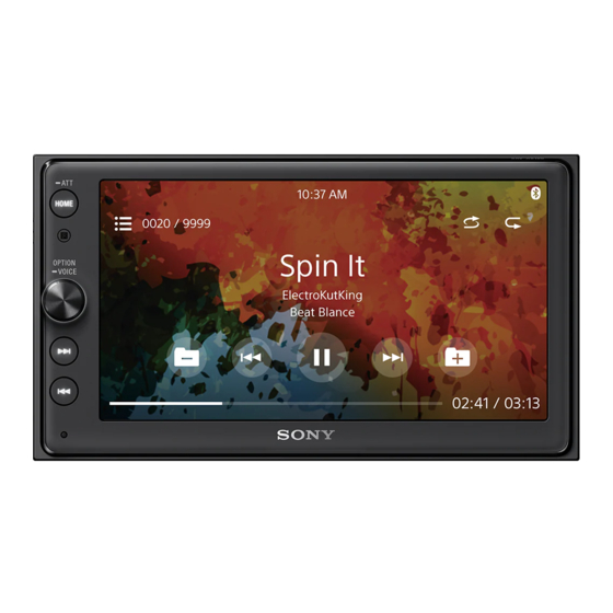
Photo: XAV-AX100
SPECIFICATIONS
Wireless communication
Communication System:
BLUETOOTH Standard version 2.1
Output:
BLUETOOTH Standard Power Class 2
(Max. +4 dBm)
Maximum communication range*
Line of sight approx. 10 m (33 ft)
Frequency band:
2.4 GHz band (2.4000 GHz – 2.4835 GHz)
Modulation method: FHSS
Compatible BLUETOOTH Profiles*
A2DP (Advanced Audio Distribution Profile) 1.2
AVRCP (Audio Video Remote Control Profile) 1.5
HFP (Handsfree Profile) 1.6
PBAP (Phone Book Access Profile) 1.1
Corresponding codec: SBC (.sbc)
)
*1 The actual range will vary depending on factors such as
obstacles between devices, magnetic fields around a
microwave oven, static electricity, reception sensitivity,
antenna (aerial)'s performance, operating system,
software application, etc.
*2 BLUETOOTH standard profiles indicate the purpose of
BLUETOOTH communication between devices.
Power amplifier section
Outputs: Speaker outputs
Speaker impedance: 4 ohms – 8 ohms
Maximum power output: 55 W × 4 (at 4 ohms)
US Model
Canadian Model
AEP Model
UK Model
Australian Model
Indian Model
XAV-AX100/AX100C2
General
Outputs:
Audio output terminals (FRONT, REAR, SUB)
Power antenna (aerial)/Power amplifier control
terminal (REM OUT)
Inputs:
1
:
Illumination control terminal
Steering control input terminal
Antenna (aerial) input terminal
Microphone input terminal
Parking brake control terminal
2
:
Reverse input terminal
Camera input terminal
USB port
Power requirements: 12 V DC car battery
(negative ground (earth))
Rated current consumption: 10 A
Dimensions: Approx. 178 mm × 100 mm × 161.5 mm
(7
1
/
in × 4 in × 6
3
/
in) (w/h/d)
8
8
Mounting dimensions:
Approx. 178 mm × 100 mm × 155 mm
(7
1
/
in × 4 in × 6
1
/
in) (w/h/d)
8
8
Mass: Approx. 1.1 kg (2 lb 7 oz)
Package contents:
Main unit (1)
Parts for installation and connections (1 set)
Remote Commander (1): RM-X170 (Except AEP, UK models)
Microphone (1)
Cable for steering wheel remote input (1)
(Indian model: Supplied to Serial No. 7104601 or larger)
Design and specifications are subject to change
without notice.
AV RECEIVER
XAV-AX100
E Model
SYS SET
Advertisement
Table of Contents

Related Manuals for Sony XAV-AX100


Summary of Contents for Sony XAV-AX100
- Page 1 Sensitivity: 44 μV 87.5 – 107.9 MHz (at 200 kHz step) FM tuning step: USB player section 50 kHz/100 kHz/200 kHz switchable Interface: USB (High-speed) Maximum current: 1.5 A AV RECEIVER 9-896-336-04 2018C33-1 Sony Video & Sound Products Inc. © 2018.03 SYS SET...
- Page 2 Bluetooth SIG, Inc. and use of such marks by Sony Corporation is under any use of such marks by Sony Corporation is under license. Other trademarks and trade names are license. Other trademarks and trade names are those of their respective owners.
-
Page 3: Table Of Contents
2018/04/20 05:03:25 (GMT+09:00) XAV-AX100/AX100C2 Ver. 1.3 TABLE OF CONTENTS SERVICING NOTES 5-15. Schematic Diagram ..........- TFT Board (5/11) (XAV-AX100) - ....... 41 5-16. Schematic Diagram GENERAL ..............10 - TFT Board (6/11) (XAV-AX100) - ....... 42 5-17. Schematic Diagram DISASSEMBLY - TFT Board (7/11) (XAV-AX100) - ....... 43 3-1. -
Page 4: Servicing Notes
2018/04/20 05:03:25 (GMT+09:00) XAV-AX100/AX100C2 Ver. 1.3 SECTION 1 SERVICING NOTES The SERVICING NOTES contains important information for servicing. Be sure to read this section before repairing the unit. UNLEADED SOLDER DESTINATION ABBREVIATIONS Boards requiring use of unleaded solder are printed with the lead- The following abbreviations for model destinations are used in this free mark (LF) indicating the solder contains no lead. - Page 5 Ver. 1.3 MODEL IDENTIFICATION DESTINATION SETTING METHOD The XAV-AX100 and XAV-AX100C2 can not be identifi ed by the (Except AX100: IND3 model) model name printed on the front panel top. When the MAIN board or U310 on the MAIN board is replaced, Be sure to refer to the model number label affi...
- Page 6 E model (E) 000003 DEST: Destination Note: Refer to “DESTINATION ABBREVIATIONS” on page 4. XAV-AX100: AEP, UK models (EUR) XAV-AX100: US, CND models (UC) 2. Confi rmation After Destination Setting XAV-AX100: E model (E) Execute the following operation after completing the destination XAV-AX100C2: E model (E) setting, and confi...
- Page 7 Checking procedure: 1. Refer to “Connection”, and connect the iPhone or Android 7. Check that this unit restarts and the logo of “SONY” is dis- phone to the main unit with USB cable. played on the screen, then turn the power off.
- Page 8 (Check that the sound output from the speak- er). (Displayed screen in the following fi gure are example) 7. Check that this unit restarts and the logo of “SONY” is dis- Picture check Sound check played on the screen, then turn the power off.
- Page 9 2018/04/20 05:03:25 (GMT+09:00) XAV-AX100/AX100C2 TOUCH PANEL ADJUST When the touch panel is replaced, perform the calibration of touch panel according to the procedure below. Procedure: 1. Turn the power on this unit. 2. Press the [HOME] button on the main unit. 3. In the state of source off (Home screen is displayed), swipe left the touch panel, and touch the [Settings] on the touch panel.
-
Page 10: General
2018/04/20 05:03:25 (GMT+09:00) XAV-AX100/AX100C2 SECTION 2 This section is extracted from GENERAL operating instruction. (US, CND models) Connection Connection/Installation Subwoofer* Cautions • Run all ground (earth) leads to a common ground (earth) point. • Do not get the leads trapped under a screw or caught in moving parts (e.g., seat railing). - Page 11 To capture your voice during handsfree calling, you need to install the microphone Mounting the unit in a Japanese car You may not be able to install this unit in some Japanese cars. In such a case, consult your Sony dealer. To the dashboard/center console Bracket...
- Page 12 2018/04/20 05:03:25 (GMT+09:00) XAV-AX100/AX100C2 (AEP, UK models) Connection Connection/Installation Subwoofer* Cautions • Run all ground (earth) leads to a common ground (earth) point. • Do not get the leads trapped under a screw or caught in moving parts (e.g., seat railing). • Before making connections, turn the car ignition Power amplifier* off to avoid short circuits.
- Page 13 Using the rear view camera You may not be able to install this unit in some Installation of the rear view camera (not supplied) is Japanese cars. In such a case, consult your Sony required before use. dealer. The image of a rear view camera connected to the...
- Page 14 2018/04/20 05:03:25 (GMT+09:00) XAV-AX100/AX100C2 Ver. 1.3 (E model) Connection Connection/Installation Subwoofer* Cautions • Run all ground (earth) leads to a common ground (earth) point. • Do not get the leads trapped under a screw or caught in moving parts (e.g., seat railing).
- Page 15 Mounting the unit in a Japanese car You may not be able to install this unit in some Japanese cars. In such a case, consult your Sony dealer. To the dashboard/center console Clip (not supplied)
- Page 16 2018/04/20 05:03:25 (GMT+09:00) XAV-AX100/AX100C2 Ver. 1.1 (IND model: Serial No. 7104600 or smaller (CABLE FOR AUTOMOBILE (RC-SR1) is not supplied)) Connection Connection/Installation Subwoofer* Cautions • Run all ground (earth) leads to a common ground (earth) point. • Do not get the leads trapped under a screw or caught in moving parts (e.g., seat railing).
- Page 17 Mounting the unit in a Japanese car You may not be able to install this unit in some Japanese cars. In such a case, consult your Sony dealer. To the dashboard/center console Clip (not supplied)
- Page 18 2018/04/20 05:03:25 (GMT+09:00) XAV-AX100/AX100C2 Ver. 1.2 (IND model: Serial No. 7104601 or larger (CABLE FOR AUTOMOBILE (RC-SR1) is supplied)) (IND3 model) Connection Connection/Installation Subwoofer* Cautions • Run all ground (earth) leads to a common ground (earth) point. • Do not get the leads trapped under a screw or caught in moving parts (e.g., seat railing).
- Page 19 To capture your voice during handsfree calling, you need to install the microphone Mounting the unit in a Japanese car You may not be able to install this unit in some Japanese cars. In such a case, consult your Sony dealer. To the dashboard/center console Bracket...
-
Page 20: Disassembly
2018/04/20 05:03:25 (GMT+09:00) XAV-AX100/AX100C2 SECTION 3 DISASSEMBLY • This set can be disassembled in the order shown below. 3-1. DISASSEMBLY FLOW Note: Due to the structure of the device, you cannot stably place it on flat surfaces. Stabilize the device by placing a stand, etc. under it that is suitable for your work. -
Page 21: Usb Cable (Usb1)
2018/04/20 05:03:25 (GMT+09:00) XAV-AX100/AX100C2 3-3. USB CABLE (USB1) 3 Remove the USB cable TFT board connector two lead pins from the groove. USB cable (CON1) front side 4 USB cable connector 5 USB cable (CON1) (USB1) TFT board front side 2 screw (PTT2.6... -
Page 22: Main Board
2018/04/20 05:03:25 (GMT+09:00) XAV-AX100/AX100C2 Ver. 1.2 3-5. MAIN BOARD Note: When the MAIN board is replaced, be sure to refer the follow- ing, and perform them. • DESTINATION SETTING METHOD (Except IND3 model) (page 5) • COMMUNICATION CHECK OF Apple CarPlay AND An- droid Auto (page 7) •... -
Page 23: Panel Bracket
2018/04/20 05:03:25 (GMT+09:00) XAV-AX100/AX100C2 3-6. PANEL BRACKET top side front side 6 panel bracket 2 three screws (PTT2.6 panel bracket sheet (blind fold) top side rear side 4 claw 3 screw 2 screw (PTT2.6 – – 1 sheet alignment mark (blind fold) -
Page 24: Tft Board
2018/04/20 05:03:25 (GMT+09:00) XAV-AX100/AX100C2 3-8. TFT BOARD Note 1: Replaced old TFT board is destroyed with the hammer, and throw out it. Note 2: When the TFT board is replaced, be sure to refer the follow- ing, and perform them. • COMMUNICATION CHECK OF Apple CarPlay OR An-... -
Page 25: Bt Antenna (Bt1), Tft (6.5) (Lcd1), Touch Panel (Tpn1)
2018/04/20 05:03:25 (GMT+09:00) XAV-AX100/AX100C2 SECTION 4 ELECTRICAL ADJUSTMENT 3-9. BT ANTENNA (BT1), TFT (6.5) (LCD1), TOUCH PANEL (TPN1) 5. Press the [OK] on the touch panel, and press the [HOME] but- MONITOR SECTION ton on the main unit, then turn the power off. -
Page 26: Diagrams
2018/04/20 05:03:25 (GMT+09:00) XAV-AX100/AX100C2 SECTION 5 DIAGRAMS 5-1. BLOCK DIAGRAM - OVERALL Section (XAV-AX100) - TOUCH iPod iPod Y1: 26MHz chip chip 6.5” BT module DRGB24bit + H/V/CLK UART CVBS Camera SPHE888 X2: 32MHz X4: 27MHz NandFlash REAR USB NandFlash Memory Video... -
Page 27: Block Diagram - Power Supply Section (Xav-Ax100)
2018/04/20 05:03:25 (GMT+09:00) XAV-AX100/AX100C2 5-2. BLOCK DIAGRAM - POWER SUPPLY Section (XAV-AX100) - Power Input POWER ANTENNA REAR NJM2816 TDA7703R (max400mA) 5V, 1.5A 7805_5V 5V,300mA BD00C0 P-AMP 8.5V/1A 1117-ADJ NJU4558 PURE5001H ML86V7675 1.5V VDD/177mA 1117-3.3 E-VOL AK7602 TVDD/16mA FLT-USB On/o L7981 SPHE888 5.5V... -
Page 28: Block Diagram - Overall Section (Xav-Ax100C2)
2018/04/20 05:03:25 (GMT+09:00) XAV-AX100/AX100C2 Ver. 1.3 5-3. BLOCK DIAGRAM - OVERALL Section (XAV-AX100C2) - TOUCH Y1: 26MHz 6.4” UART DRGB24bit + H/V/CLK BT module CVBS Camera SPHE888 X2: 32MHz X4: 27MHz Nand Flash NandFlash NandFlash REAR USB Memory Video CCIR656 Decoder SPHE8388... -
Page 29: Block Diagram - Power Supply Section (Xav-Ax100C2)
2018/04/20 05:03:25 (GMT+09:00) XAV-AX100/AX100C2 Ver. 1.3 5-4. BLOCK DIAGRAM - POWER SUPPLY Section (XAV-AX100C2) - Power Input POWER ANTENNA REAR NJM2816 TDA7703R (max400mA) 5V,1.5A 7805 _5V V 5V,300mA BD00C0 P-AMP 8.5V/1A 1117-ADJ NJU4558 PURE5001H ML86V7675 1.5V 1.5V LPF/RCL 1117 -3.3 E-VOL VDD/177mA... - Page 30 2018/04/20 05:03:25 (GMT+09:00) XAV-AX100/AX100C2 Ver. 1.2 THIS NOTE IS COMMON FOR PRINTED WIRING BOARDS AND SCHEMATIC DIAGRAMS. • IC Pin Function Description (In addition to this, the necessary note is printed in each block.) MAIN BOARD U310 STM8S207CBT (ST07) (SYSTEM CONTROLLER) For Printed Wiring Boards.
-
Page 31: Schematic Diagram - Main Board (1/3)
2018/04/20 05:03:25 (GMT+09:00) XAV-AX100/AX100C2 5-5. SCHEMATIC DIAGRAM - MAIN Board (1/3) - MAIN BOARD (1/3) XAV-AX100/AX100C2 SYS SET... -
Page 32: Schematic Diagram - Main Board (2/3)
2018/04/20 05:03:25 (GMT+09:00) XAV-AX100/AX100C2 Ver. 1.2 5-6. SCHEMATIC DIAGRAM - MAIN Board (2/3) - • See page 30 for IC Pin Function Description. MAIN BOARD (2/3) Note: When the U310 on the MAIN board is replaced, be sure to refer the “DESTINATION SETTING METHOD (Except IND3 model)”... -
Page 33: Schematic Diagram - Main Board (3/3)
2018/04/20 05:03:25 (GMT+09:00) XAV-AX100/AX100C2 5-7. SCHEMATIC DIAGRAM - MAIN Board (3/3) - MAIN BOARD (3/3) XAV-AX100/AX100C2 SYS SET... -
Page 34: Printed Wiring Board - Main Board (Component Side)
2018/04/20 05:03:25 (GMT+09:00) XAV-AX100/AX100C2 Ver. 1.3 5-8. PRINTED WIRING BOARD - MAIN Board (Component Side) - • : Uses unleaded solder. MAIN BOARD (COMPONENT SIDE) Note: When the U310 on the MAIN board is replaced, be sure to refer the “DESTINATION SETTING METHOD (Except IND3 model)” on page 5, and perform it. -
Page 35: Main Board (Conductor Side)
2018/04/20 05:03:25 (GMT+09:00) XAV-AX100/AX100C2 Ver. 1.3 5-9. PRINTED WIRING BOARD - MAIN Board (Conductor Side) - • : Uses unleaded solder. MAIN BOARD (CONDUCTOR SIDE) XAV-AX100/AX100C2 SYS SET... -
Page 36: 5-10. Printed Wiring Board - Tft Board
2018/04/20 05:03:25 (GMT+09:00) XAV-AX100/AX100C2 Ver. 1.3 5-10. PRINTED WIRING BOARD - TFT Board - • : Uses unleaded solder. TFT BOARD (COMPONENT SIDE) TFT BOARD (CONDUCTOR SIDE) XAV-AX100/AX100C2 SYS SET... -
Page 37: Schematic Diagram - Tft Board (1/11) (Xav-Ax100)
2018/04/20 05:03:25 (GMT+09:00) XAV-AX100/AX100C2 5-11. SCHEMATIC DIAGRAM - TFT Board (1/11) (XAV-AX100) - TFT BOARD (1/11) CON7 [2,3,4,8,12] R261 PWR_3V3 [3,10,12] TFT_6V CON2 R304 R122 PIN10 VLED+ MCU_SCL VLED+ R295 R111 VLED+ R265 MCU_SDA CORE_5V VLED- VLED- R263 R286 UA4_RX VLED- R303... -
Page 38: Schematic Diagram - Tft Board (2/11) (Xav-Ax100)
2018/04/20 05:03:25 (GMT+09:00) XAV-AX100/AX100C2 5-12. SCHEMATIC DIAGRAM - TFT Board (2/11) (XAV-AX100) - TFT BOARD (2/11) [2,3,10,12] TFT_6V [9,10] TFT VGL & VGH & AVDD_10V4 AK_VDD_3V3 TP10 1117-3.3A VGH_16V 560R VGL_-7V ASP_GND BAV99 ASP_GND HL_GND HL_GND [2,3,10,12] TFT_6V [2,3,10,12] TFT_6V TP11 2.7uH... -
Page 39: Schematic Diagram - Tft Board (3/11) (Xav-Ax100)
2018/04/20 05:03:25 (GMT+09:00) XAV-AX100/AX100C2 5-13. SCHEMATIC DIAGRAM - TFT Board (3/11) (XAV-AX100) - TFT BOARD (3/11) [4,7,8,9] CORE_3V3 [4,7,8,9] PWR_1V1 [4,5,7] CORE_1V1 CORE_3V3 10uH AVDD33 TP14 FB17 USB0VDD33 3.3uH TPS_5V VIN1 PWR_1V1 R206 VIN2 BST1 VIN3 VINQ DC_GND 10uH COMP1 PLL_VDD33 FB18... -
Page 40: Schematic Diagram - Tft Board (4/11) (Xav-Ax100)
2018/04/20 05:03:25 (GMT+09:00) XAV-AX100/AX100C2 5-14. SCHEMATIC DIAGRAM - TFT Board (4/11) (XAV-AX100) - TFT BOARD (4/11) [4,5,7] [4,5] CORE_1V1 AVDD33 PLL_VDD33 PLLC_AVDD PLL_AVDD PLL_1V2 [4,5,7] VDD11 CORE_1V1 VDD11 VDD11 [4,5] VDD11 AVDD33 VDD11 VDD11 VDD11 VDD11 VDD11 VDD11 U1-G VDD11 AR1668 VDD11... -
Page 41: Schematic Diagram - Tft Board (5/11) (Xav-Ax100)
2018/04/20 05:03:25 (GMT+09:00) XAV-AX100/AX100C2 5-15. SCHEMATIC DIAGRAM - TFT Board (5/11) (XAV-AX100) - TFT BOARD (5/11) [4,6] [4,6] DDR_1V5 DDR_1V5 U1-A R238 A_RMA0 A_A0 A_D0 A_RMD0 R236 A_RMA1 A_A1 A_D1 A_RMD1 R226 A_A2 A_D2 A_RMA2 A_RMD2 R229 A_A3 A_D3 A_RMA3 A_RMD3 R231... -
Page 42: Schematic Diagram - Tft Board (6/11) (Xav-Ax100)
2018/04/20 05:03:25 (GMT+09:00) XAV-AX100/AX100C2 5-16. SCHEMATIC DIAGRAM - TFT Board (6/11) (XAV-AX100) - TFT BOARD (6/11) U1-F [4,7,8,9] NF_RDY0 NAND_RDY UA0_TX/GPIO[91] UA0_TX Debug [4,7] NAND FLASH CORE_3V3 NAND_RE_B UA0_RX/GPIO[92] NF_RE_B UA0_RX NAND_3V3 NF_CE0_B NAND_CE0_B R190 NF_CLE NAND_CLE UA1_TX//GPIO[85] UA1_TX UA1_TX R175 NAND_ALE... -
Page 43: Schematic Diagram - Tft Board (7/11) (Xav-Ax100)
2018/04/20 05:03:25 (GMT+09:00) XAV-AX100/AX100C2 5-17. SCHEMATIC DIAGRAM - TFT Board (7/11) (XAV-AX100) - TFT BOARD (7/11) U1-B AA21 DP_R[0] DP_R[0] AB13 I2C0_SCL SCL0/GPIO[22] DP_R[1] DP_R[1] AA13 AB15 SDA0/GPIO[23] R2/LVDS_TXB0 I2C0_SDA DP_R[2] AA15 R3LVDS_TX0 RF Path Impedance:50 DP_R[3] AB16 R4/LVDS_TXB1 DP_R[4] AA16 (ANT->SE4150 PIN4_LNA_IN) -
Page 44: Schematic Diagram - Tft Board (8/11) (Xav-Ax100)
2018/04/20 05:03:25 (GMT+09:00) XAV-AX100/AX100C2 5-18. SCHEMATIC DIAGRAM - TFT Board (8/11) (XAV-AX100) - TFT BOARD (8/11) U1-C U1-D AOUT_L0 CORE_AL0 AIN_L0 AIN_L0 ADAC_VLPC0L LDSW SVOTST7/LDSW C232 AIN_R0 AOUT_R0 AUOUT_R0 HOME SVOTST1 AIN_R0 V165 V165 AIN_L1 ADAC_VLPC0R SVOTST2 AIN_L1 TRAY- C220 CON8 DA_TEO/GPIO[102]... -
Page 45: Schematic Diagram - Tft Board (9/11) (Xav-Ax100)
2018/04/20 05:03:25 (GMT+09:00) XAV-AX100/AX100C2 5-19. SCHEMATIC DIAGRAM - TFT Board (9/11) (XAV-AX100) - TFT BOARD (9/11) [3,10] AK_3V3 [3,9,10] R105 AK_VDD_3V3 ASP_GND [10] AK_RST ASP_GND [3,10] AK_3V3 [10] MUTEN AK_MUTE ASP_GND 1uF/25V/X7R C116 RADIO_AL AINL1 AOUT1L AOUT_FL C117 1uF/25V/X7R GNDIN1 AOUT1R AOUT_FR... -
Page 46: Schematic Diagram - Tft Board (10/11) (Xav-Ax100)
2018/04/20 05:03:25 (GMT+09:00) XAV-AX100/AX100C2 5-20. SCHEMATIC DIAGRAM - TFT Board (10/11) (XAV-AX100) - TFT BOARD (10/11) [3,11] C_1V5 DGND DGND [11] [3,11] MLV_D_3V3 ML86_RST R221 GPIO33 [11] GIN1 GIN1 RESETN [11] ML86_RST [11] STATUS GIN2 TP20 [11] CLKO ML8_CLK [3,11] MLV_3V3 AVDD... -
Page 47: Schematic Diagram - Tft Board (11/11) (Xav-Ax100)
2018/04/20 05:03:25 (GMT+09:00) XAV-AX100/AX100C2 5-21. SCHEMATIC DIAGRAM - TFT Board (11/11) (XAV-AX100) - TFT BOARD (11/11) CON3 [12] [12] BT_ANT USB0_DP 0.5PF USB0_DM [12] USB_5V [12] [2,3,10,12] USB_5V [2,3,10,12] [12] TFT_6V 4Pin-2.0 TFT_6V VOUT USB_5V CON9 [12] [12] USB_EN CONT VOADJ BT_ANT... -
Page 48: Schematic Diagram - Tft Board (1/11) (Xav-Ax100C2)
2018/04/20 05:03:25 (GMT+09:00) XAV-AX100/AX100C2 Ver. 1.3 5-22. SCHEMATIC DIAGRAM - TFT Board (1/11) (XAV-AX100C2) - TFT BOARD (1/11) CON7 [2,3,4,8,12] PWR_3V3 R261 0.1R TFT_6V [3,10,12] CON2 R304 R122 PIN10 MCU_SCL VLED+ VLED+ R295 R111 R265 VLED+ MCU_SDA CORE_5V R263 VLED- VLED- R286... -
Page 49: Schematic Diagram - Tft Board (2/11) (Xav-Ax100C2)
2018/04/20 05:03:25 (GMT+09:00) XAV-AX100/AX100C2 Ver. 1.3 5-23. SCHEMATIC DIAGRAM - TFT Board (2/11) (XAV-AX100C2) - TFT BOARD (2/11) [2,3,10,12] TFT_6V [9,10] T F T V G L & V G H & A V D D _10V 4 AK_VDD_3V3 TP10 1117-3.3A VGH_16V... -
Page 50: Schematic Diagram - Tft Board (3/11) (Xav-Ax100C2)
2018/04/20 05:03:25 (GMT+09:00) XAV-AX100/AX100C2 Ver. 1.3 5-24. SCHEMATIC DIAGRAM - TFT Board (3/11) (XAV-AX100C2) - TFT BOARD (3/11) [4,7,8,9] CORE_3V3 PWR_1V1 [4,7,8,9] CORE_1V1 [4,5,7] CORE_3V3 10uH AVDD33 FB17 TP14 USB0VDD33 3.3uH TPS_5V VIN1 PWR_1V1 R206 47nF VIN2 BST1 10K/1% VIN3 VINQ DC_GND... -
Page 51: Schematic Diagram - Tft Board (4/11) (Xav-Ax100C2)
2018/04/20 05:03:25 (GMT+09:00) XAV-AX100/AX100C2 Ver. 1.3 5-25. SCHEMATIC DIAGRAM - TFT Board (4/11) (XAV-AX100C2) - TFT BOARD (4/11) [4,5,7] CORE_1V1 [4,5] AVDD33 PLL_VDD33 PLLC_AVDD PLL_AVDD PLL_1V2 [4,5,7] VDD11 CORE_1V1 VDD11 VDD11 [4,5] VDD11 AVDD33 VDD11 VDD11 VDD11 VDD11 VDD11 VDD11 U1-G VDD11... -
Page 52: Schematic Diagram - Tft Board (5/11) (Xav-Ax100C2)
2018/04/20 05:03:25 (GMT+09:00) XAV-AX100/AX100C2 Ver. 1.3 5-26. SCHEMATIC DIAGRAM - TFT Board (5/11) (XAV-AX100C2) - TFT BOARD (5/11) [4,6] [4,6] DDR_1V5 DDR_1V5 U1-A R238 A_RMA0 A_A0 A_D0 A_RMD0 R236 A_RMA1 A_A1 A_D1 A_RMD1 R226 A_RMA2 A_A2 A_D2 A_RMD2 R229 A_RMA3 A_A3 A_D3... -
Page 53: Schematic Diagram - Tft Board (6/11) (Xav-Ax100C2)
2018/04/20 05:03:25 (GMT+09:00) XAV-AX100/AX100C2 Ver. 1.3 5-27. SCHEMATIC DIAGRAM - TFT Board (6/11) (XAV-AX100C2) - TFT BOARD (6/11) U1-F NF_RDY0 NAND_RDY UA0_TX/GPIO[91] UA0_TX D ebug [4,7,8,9] [4,7] N A N D F LA S H CORE_3V3 NF_RE_B NAND_RE_B UA0_RX/GPIO[92] UA0_RX NAND_3V3 NF_CE0_B... -
Page 54: Schematic Diagram - Tft Board (7/11) (Xav-Ax100C2)
2018/04/20 05:03:25 (GMT+09:00) XAV-AX100/AX100C2 Ver. 1.3 5-28. SCHEMATIC DIAGRAM - TFT Board (7/11) (XAV-AX100C2) - TFT BOARD (7/11) U1-B AA21 DP_R[0] DP_R[0] AB13 I2C0_SCL SCL0/GPIO[22] DP_R[1] DP_R[1] AA13 AB15 I2C0_SDA SDA0/GPIO[23] R2/LVDS_TXB0 DP_R[2] AA15 R3LVDS_TX0 DP_R[3] RF Path AB16 R4/LVDS_TXB1 DP_R[4] AA16 (ANT->SE4150 PIN4_LNA_IN) -
Page 55: Schematic Diagram - Tft Board (8/11) (Xav-Ax100C2)
2018/04/20 05:03:25 (GMT+09:00) XAV-AX100/AX100C2 Ver. 1.3 5-29. SCHEMATIC DIAGRAM - TFT Board (8/11) (XAV-AX100C2) - TFT BOARD (8/11) U1-C U1-D AOUT_L0 CORE_AL0 AIN_L0 LDSW AIN_L0 ADAC_VLPC0L SVOTST7/LDSW C232 0.1uF AUOUT_R0 HOME AIN_R0 AIN_R0 AOUT_R0 SVOTST1 V165 V165 TRAY- AIN_L1 AIN_L1 ADAC_VLPC0R SVOTST2 C220 0.1uF... -
Page 56: Schematic Diagram - Tft Board (9/11) (Xav-Ax100C2)
2018/04/20 05:03:25 (GMT+09:00) XAV-AX100/AX100C2 Ver. 1.3 5-30. SCHEMATIC DIAGRAM - TFT Board (9/11) (XAV-AX100C2) - TFT BOARD (9/11) [3,10] AK_3V3 [3,9,10] R105 AK_VDD_3V3 ASP_GND [10] AK_RST ASP_GND [3,10] AK_3V3 AK_MUTE MUTEN ASP_GND [10] 1uF/25V/X7R C116 RADIO_AL AINL1 AOUT1L AOUT_FL C117 1uF/25V/X7R ASP_GND... -
Page 57: Schematic Diagram - Tft Board (10/11) (Xav-Ax100C2)
2018/04/20 05:03:25 (GMT+09:00) XAV-AX100/AX100C2 Ver. 1.3 5-31. SCHEMATIC DIAGRAM - TFT Board (10/11) (XAV-AX100C2) - TFT BOARD (10/11) [3,11] C_1V5 DGND DGND [11] [3,11] MLV_D_3V3 ML86_RST R221 GPIO33 [11] GIN1 GIN1 RESETN ML86_RST [11] [11] STATUS TP20 GIN2 CLKO ML8_CLK [11] [3,11]... -
Page 58: Schematic Diagram - Tft Board (11/11) (Xav-Ax100C2)
2018/04/20 05:03:25 (GMT+09:00) XAV-AX100/AX100C2 Ver. 1.3 5-32. SCHEMATIC DIAGRAM - TFT Board (11/11) (XAV-AX100C2) - TFT BOARD (11/11) CON3 [12] [12] BPF-1608-2.45G BT_ANT R115 USB0_DP R128 USB0_DM [12] USB_5V [12] [2,3,10,12] USB_5V [2,3,10,12] [12] TFT_6V 4Pin-2.0 TFT_6V VOUT USB_5V CON9 C360 [12]... -
Page 59: Exploded Views
2018/04/20 05:03:25 (GMT+09:00) XAV-AX100/AX100C2 Ver. 1.3 SECTION 6 EXPLODED VIEWS Note: • -XX and -X mean standardized parts, so • The mechanical parts with no reference they may have some difference from the number in the exploded views are not sup- original one. -
Page 60: Front Panel Section
2018/04/20 05:03:25 (GMT+09:00) XAV-AX100/AX100C2 Ver. 1.3 6-2. FRONT PANEL SECTION front side TPN1 LCD1 not supplied not supplied rear side Note 1: Replaced old complete TFT board (Ref. No. 54) is destroyed Note 3: When the TFT (6.5) (Ref. No. LCD1) is replaced, refer to with the hammer, and throw out it. -
Page 61: Electrical Parts List
2018/04/20 05:03:25 (GMT+09:00) XAV-AX100/AX100C2 Ver. 1.3 SECTION 7 MAIN ELECTRICAL PARTS LIST Note: • Due to standardization, replacements in • CAPACITORS When indicating parts by reference num- uF: μF the parts list may be different from the ber, please include the board name. - Page 62 2018/04/20 05:03:25 (GMT+09:00) XAV-AX100/AX100C2 Ver. 1.3 Ref. No. Part No. Description Remark PARTS FOR INSTALLATION AND CONNECTIONS ************************************** (AX100: AEP, UK) X-2594-046-1 FRAME, FITTING ASSY (Bracket) (AX100: AEP, UK) 4-479-204-01 RELEASE KEY (1 piece) (AX100: AEP, UK) 4-597-040-01 COLLAR, HARD (Hard type Collar)
- Page 63 2018/04/20 05:03:25 (GMT+09:00) XAV-AX100/AX100C2 MEMO SYS SET...
- Page 64 Change of Part No. for OPERATING INSTRUCTION (E) Change of Part for MICROPHONE UNIT (Ref. No. 506) (SMR-17006) 2017.06 Addition of IND3 model 2018.03 Addition of XAV-AX100C2 Change of printed wiring board Change of Part No. for OPERATING INSTRUCTION (XAV-AX100: AEP, UK) (SMR-17048) SYS SET...